Товары (35.000+)

TMS320F28335 - C2000 32-Bit DSC 150MHz FPU 512KB | TI
TMS320F28335

TMS320F28335 - C2000 32-Bit DSC 150MHz FPU 512KB | TI

The Texas Instruments TMS320F28335 is a C2000 Delfino 32-bit floating-point digital signal controller (DSC) delivering 150 MIPS (150 MHz CPU clock), 512 KB (256K x 16) of on-chip Flash, an external memory interface (EMIF), and a 12-bit ADC, housed in a 176-pin LQFP package (PGF suffix). A digital signal controller combines the computational throughput of a digital signal processor with the peripheral integration and control-oriented architecture of a microcontroller. Within the power management hierarchy, the DSC sits at the top of the C2000 real-time controller family: MCU -> digital signal controller -> embedded processor -> semiconductor device, making it the central control element in digitally controlled power and motion systems. Key features include the 32-bit C28x CPU core with an integrated single-precision FPU, which removes the software overhead of fixed-point arithmetic for control-law computations; 150 MIPS sustained real-time performance; 512 KB Flash with 34K x 16 bytes of SARAM for code and data; 18 PWM channels including high-resolution ePWM for power conversion; and a rich analog and communications suite with 12-bit ADC, eCAN, McBSP, SPI, SCI, and I2C interfaces. Architecturally, the TMS320F28335 uses a modified Harvard bus structure with separate program and data buses, a unified memory map enabled by the FPU generation, a 32 x 32-bit multiplier, atomic read-modify-write instructions, and fast interrupt latency suited to field-oriented motor control loops running in the tens of microseconds. Three 32-bit CPU timers and a PIE interrupt matrix support deterministic real-time execution. Typical applications include industrial motor drives (FOC for PMSM and induction motors), digital power supplies and solar inverters, and automotive/transportation control systems where high-resolution PWM and fast ADC feedback loops are mandatory. A key design consideration: at 150 MHz, the core voltage supply differs from the I/O supply, so dual-rail power sequencing and proper decoupling per the TI TMS320x2833x Technical Reference Manual are essential for reliable operation. This page synthesizes verified distributor data, drop-in same-family alternatives, and practical design guidance beyond what the manufacturer datasheet page alone provides.

Запрос цены Контакты
TMS320F28335PGFA - 150MHz 32-bit C2000 DSC MCU | Texas Instruments
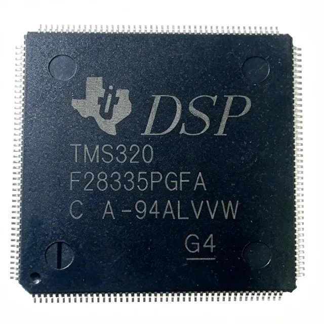
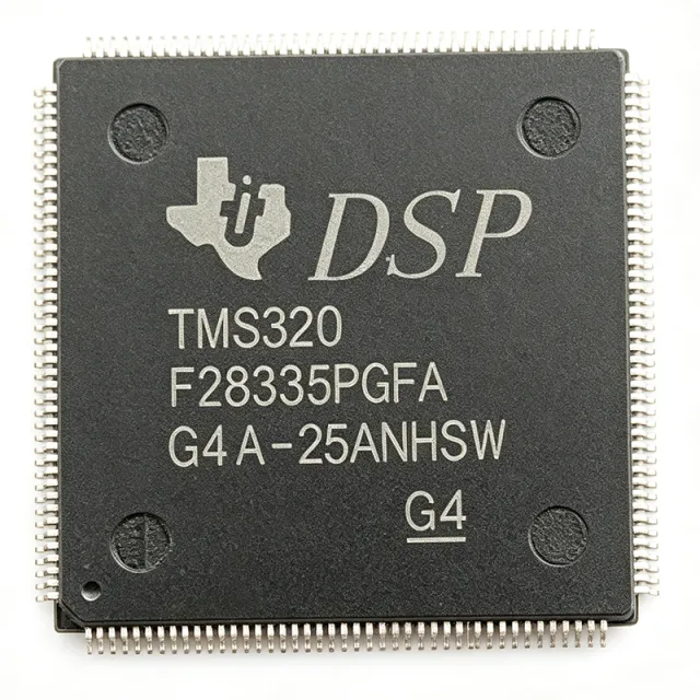
TMS320F28335PGFA

TMS320F28335PGFA - 150MHz 32-bit C2000 DSC MCU | Texas Instruments

The Texas Instruments TMS320F28335PGFA is a 32-bit floating-point digital signal controller (DSC) from the C2000 Delfino family, delivering 150 MHz (150 MIPS) performance with 512 KB (256K x 16) on-chip flash memory and 68 KB SRAM, housed in a 176-pin LQFP (24x24 mm, PGF) surface-mount package. A digital signal controller combines the real-time control capability of a microcontroller (MCU) with the mathematical throughput of a digital signal processor (DSP). Within the embedded control hierarchy, the C2000 Delfino DSC sits at the top of real-time controllers, above generic MCUs, for closed-loop control loops running at tens of kilohertz. The C28x core uses a Harvard architecture with a hardware multiplier and a single-precision floating-point unit (FPU) that accelerates field-oriented control (FOC) and other complex control algorithms. Key features include a 12-bit ADC with up to 16 channels, 18 PWM outputs including high-resolution PWM (HRPWM), and communication peripherals covering CAN, SPI, SCI (UART), and I2C. An external memory interface (EMIF) expands memory beyond on-chip resources, a differentiator versus smaller C2000 parts such as the TMS320F28027. The device is fabricated on TI 180 nm CMOS process technology. It runs from a 1.9 V core supply and 3.3 V I/O supply, with typical power consumption near 300 mW at full speed, and operates from -40C to +85C, qualifying it for industrial environments. The FPU executes single-cycle floating-point operations, critical for high-speed control loops without fixed-point IQmath conversion. Typical applications include servo motor drives, solar inverters, digital power supplies, and industrial automation where fast ADC sampling and precise PWM edges are essential. Design consideration: decouple the 1.9 V core and 3.3 V I/O rails separately, budget for LQFP thermal dissipation, and use the JTAG port with Code Composer Studio for real-time emulation and debugging. This page synthesizes distributor pricing, verified drop-in alternatives, and practical design notes not found in the manufacturer datasheet alone.

USD $14,20 Контакты
TMS320F28335PTPQ - 150MHz C2000 DSC MCU, 512KB Flash | TI
TMS320F28335PTPQ

TMS320F28335PTPQ - 150MHz C2000 DSC MCU, 512KB Flash | TI

The Texas Instruments TMS320F28335PTPQ is an automotive-qualified C2000 Delfino 32-bit digital signal controller (DSC) running at 150 MHz with a hardware floating-point unit, 512KB (256K x 16) of flash memory, and a 176-pin HLQFP (PTP) package rated from -40C to +125C. A digital signal controller combines the computational throughput of a digital signal processor with the peripheral integration of a microcontroller. In the embedded control hierarchy, the C2000 Delfino family sits at TI's high-performance real-time control tier, positioned above general-purpose MCUs and alongside dedicated DSPs. These devices are engineered specifically for closed-loop control systems where fast math and precise analog feedback are critical. Key features include 150 MIPS C28x CPU performance with a hardware FPU for executing complex control laws, 512KB of flash with 68KB of SRAM, and an external memory interface (EMIF) for memory expansion. A 12-bit, 16-channel ADC provides high-resolution conversion for motor current and voltage sensing, while up to 18 PWM outputs deliver precise power-stage switching timing. Architecturally, the C28x core uses a modified Harvard bus structure enabling simultaneous instruction and data fetches. Six-channel DMA offloads the CPU for data movement, and the ADC and PWM modules are synchronized for deterministic control-loop execution. A code security module, watchdog timer, and real-time interrupt support robust operation in safety-critical powertrain systems. Typical applications include automotive traction inverters, electric power steering, industrial servo drives, solar inverters, and digital power supplies. AEC-Q100 Grade 1 qualification makes the device suitable for under-hood environments where reliability is paramount. Designers should budget for dual-rail power (1.9V core, 3.3V I/O) with careful decoupling, provide a clean analog supply and reference for full 12-bit ADC accuracy, and configure flash wait states correctly at 150 MHz for optimal performance. This page synthesizes manufacturer datasheet data, distributor pricing, drop-in replacement information, and practical design notes in a single resource not available in the raw datasheet.

USD $35,20 Контакты
TMS320F28335QPGFAQ1 - 150MHz C2000 Delfino MCU Q1 | Texas Instruments
TMS320F28335QPGFAQ1

TMS320F28335QPGFAQ1 - 150MHz C2000 Delfino MCU Q1 | Texas Instruments

The Texas Instruments TMS320F28335QPGFAQ1 is an automotive-grade (AEC-Q100 qualified) C2000 Delfino 32-bit real-time microcontroller delivering 150 MIPS with an integrated single-precision FPU, 512 KB (256K x 16) of on-chip flash, EMIF external memory interface, and a 12-bit ADC, housed in a 176-pin LQFP (24x24 mm) package. A digital signal controller (DSC) is a hybrid of a microcontroller (MCU) and a digital signal processor (DSP): it combines flash memory, communication peripherals, and control peripherals with DSP-class math capability. In the hierarchy of embedded processors, the TMS320F28335QPGFAQ1 sits within TI's C2000 real-time control MCU family, which is optimized for processing, sensing, and actuation to improve closed-loop performance in real-time control systems. Key features include the 32-bit C28x core running at 150 MHz with 32x32-bit MAC operations, a single-precision floating-point unit (FPU) for fast control-law computation, 18 PWM outputs for power conversion and motor control, and an external memory interface (EMIF) for expansion. The 12-bit, 16-channel ADC provides fast, precise sensing for current and voltage feedback loops. Automotive qualification makes the device suited to harsh environments with extended temperature support. The architecture integrates control peripherals with the C28x core so that sensing-to-actuation latency is minimized, a critical factor in digital power and motor drives where loop bandwidth determines system performance. Flash-based programmability allows field updates without external memory. Typical applications include industrial motor drives, solar inverters and digital power, electric vehicles and transportation systems, and sensing and signal processing. Design tip: manage flash wait-states at 150 MHz operation and follow TI's power-supply sequencing guidance for the dual-rail 1.9V core and 3.3V I/O domains. Pricing below is as of 2026-08-29.

Запрос цены Контакты
TMS320F28343-Q1 - C2000 Delfino MCU | Texas Instruments
TMS320F28343-Q1

TMS320F28343-Q1 - C2000 Delfino MCU | Texas Instruments

The TMS320F28343-Q1 is an automotive-grade real-time microcontroller from Texas Instruments, part of the C2000 Delfino family. The C2000 line is optimized for processing, sensing, and actuation to improve closed-loop performance in real-time control applications such as industrial motor drives, solar inverters and digital power, electrical vehicles and transportation, motor control, and sensing and signal processing. The device is built around the C28x DSP core, which provides 32-bit processing and a floating-point unit for high-precision control algorithms. The C2000 real-time microcontrollers are designed for the most demanding real-time control tasks, offering a rich set of peripherals including PWM modules, ADCs, and communication interfaces. As of our verification date, the full specifications for the TMS320F28343-Q1 were not available in our verified web data. Engineers should consult the official TI datasheet for complete parameters, including clock speed, flash memory, package, and pinout. The TMS320F28343-Q1 is a member of the Delfino family, which is positioned as a premium performance MCU line within C2000. It is intended for applications that require high precision, fast loop rates, and robust operation in harsh environments. The device is supplied in a package that is yet to be confirmed, but typical Delfino parts use 176-pin LQFP or BGA options. For design, it is important to consider the thermal requirements and power supply decoupling. The wide operating temperature range of the Q1 variant enables use in automotive powertrain and chassis control. While specific electrical characteristics are unknown, the architecture ensures that software developed for other Delfino devices, such as the TMS320F28335, can be ported with minor changes. This makes it a flexible option for projects migrating from older C2000 controllers. However, before production, designers must obtain the exact datasheet and verify the pinout, memory sizes, and peripheral set to ensure compatibility with the target application.

Запрос цены Контакты
TMS320F28346-Q1 - 300MHz C2000 Delfino MCU | Texas Instruments
TMS320F28346-Q1

TMS320F28346-Q1 - 300MHz C2000 Delfino MCU | Texas Instruments

The TMS320F28346-Q1 is a C2000 Delfino 32-bit microcontroller from Texas Instruments designed for high-performance real-time control applications. Featuring a C28x core running at 300 MHz, it delivers 300 MIPS of processing power with an integrated floating-point unit (FPU) to accelerate complex mathematical operations. The device includes 516 KB of RAM for data and program storage and an external memory interface (EMIF) that allows expansion with external SRAM or flash. It is available in a 256-ball BGA (17x17 mm) package, suitable for surface-mount assembly. A microcontroller (MCU) is a compact integrated circuit designed to execute a specific application. It typically contains a processor core, memory, and programmable input/output peripherals. In the system hierarchy, an MCU is a type of digital signal processor-capable computing device that bridges the gap between simple microprocessors and full SoCs. The C2000 series specializes in real-time control, positioning this device in the power management IC and industrial automation domain. Key features include the 300 MHz C28x CPU, the FPU that accelerates floating-point operations, 516 KB RAM for large data buffers, and EMIF for external memory. The automotive-grade Q1 designation ensures AEC-Q100 qualification, making it suitable for use in vehicular environments. The device targets applications that require deterministic, low-latency control processing. In terms of technical depth, the C28x architecture is optimized for control algorithms, with separate accumulator paths for improved instruction efficiency. The FPU supports single-precision IEEE 754 operations, beneficial for control loops and FFT computations. The EMIF provides a configurable interface to various memory types, enabling flexibility in system design. Typical applications include automotive traction motor control, industrial servo drives, digital power converters, and renewable energy inverters. The combination of high MIPS, FPU, and large RAM makes it ideal for field-oriented control (FOC) of PMSMs, multi-loop power converter control, and complex filtering tasks. When designing with this device, ensure proper decoupling near power pins and adequate thermal management for the 256-ball BGA package. The enable pin and reset circuitry must be designed for reliable power-up sequencing. [DATA_NEEDED: specific reference design]

Запрос цены Контакты
TMS320F28374SPTPS - 200MHz C2000 MCU | Texas Instruments
TMS320F28374SPTPS

TMS320F28374SPTPS - 200MHz C2000 MCU | Texas Instruments

The TMS320F28374SPTPS is a high-performance 32-bit microcontroller from Texas Instruments' C2000 Delfino family, designed for advanced closed-loop control applications. It features a C28x CPU core running at 200 MHz, delivering 400 MIPS, and includes a Control Law Accelerator (CLA), floating-point unit (FPU), and trigonometric math unit (TMU). The device integrates 512 KB of flash memory (256K x 16) and is packaged in a 176-pin HLQFP (PTP) package with exposed pad. A microcontroller (MCU) is a compact integrated circuit designed to govern a specific operation in an embedded system. It contains a processor core, memory, and programmable input/output peripherals. The C2000 family is a series of MCUs optimized for real-time control, combining the processing power of a digital signal processor with the peripherals of a microcontroller. This makes them ideal for applications requiring precise, high-speed calculations and control loops. Key features include a 12-bit ADC, multiple communication interfaces (SCI, SPI, I2C, CAN), and enhanced PWM modules. The device supports functional safety (FuSa) applications, making it suitable for automotive and industrial systems. The 176-pin HLQFP package provides ample I/O for complex control systems. The TMS320F28374S architecture includes a dual-core option (TMS320F28374D) and a single-core variant, with the 'S' denoting single-core. The CLA is a parallel processing unit that can execute control algorithms independently, offloading the main CPU. The FPU and TMU accelerate mathematical operations, crucial for real-time control algorithms. Typical applications include industrial motor drives, solar inverters, electric vehicle powertrains, and digital power supplies. The device's high-speed ADC and PWM modules enable precise current and voltage sensing and control. When designing with this MCU, ensure proper decoupling of the 1.2V core supply and use the internal voltage regulator. The exposed pad must be soldered to the PCB ground plane for thermal management.

Запрос цены Контакты
TMS320F28376S - 400 MIPS C2000 MCU 512KB Flash | Texas Instruments
TMS320F28376S

TMS320F28376S - 400 MIPS C2000 MCU 512KB Flash | Texas Instruments

The Texas Instruments TMS320F28376S is a Delfino C2000 32-bit real-time microcontroller delivering 400 MIPS from a single C28x CPU core at 200 MHz, with 512 KB flash, a Control Law Accelerator (CLA), FPU, TMU, EMIF, and 16-bit ADC, packaged in a 176-pin HLQFP (PTP). A real-time microcontroller is a processor class designed to execute closed-loop control algorithms with deterministic timing. The C2000 Delfino family sits between general-purpose MCUs and high-performance DSPs in the embedded-processor hierarchy, combining a fast core with tightly integrated PWM and ADC peripherals purpose-built for motor control, digital power, and renewable energy systems. Key features include the 200 MHz C28x Harvard-architecture CPU with hardware FPU and Trigonometric Math Unit (TMU), a dedicated CLA that independently executes control loops offloaded from the main CPU, 512 KB of on-chip flash, and a 16-bit ADC with 12-bit mode options for high-precision sensing. External Memory Interface (EMIF) support enables expansion, and connectivity spans CAN, I2C, SPI, SCI, and USB. Architecturally, the C28x core enables simultaneous instruction and data fetches, while the FPU and TMU accelerate floating-point and trigonometric math essential for Field-Oriented Control (FOC) and power-conversion algorithms. A programmable control law accelerator supports custom logic acceleration, reducing CPU interrupt latency in fast control loops. Typical applications include industrial servo drives, solar inverters, digital power supplies, electric vehicle and transportation systems, and power line communications. The 400 MIPS rating and integrated 16-bit ADC support high-bandwidth control loops without external signal-chain components. Design tip: decouple all power pins, follow the datasheet ADC layout guidelines, and solder the exposed thermal pad for proper heat dissipation. Choose the single-CPU TMS320F28376S for cost-optimized designs; the pin-compatible TMS320F28377S adds dual CPUs when more performance headroom is required. This page synthesizes distributor pricing, drop-in alternatives, comparison data, and practical design notes not found in the manufacturer datasheet alone.

Запрос цены Контакты
TMS320F28376SQ-Q1 - 200MHz C2000 Delfino AEC-Q100 MCU | TI
TMS320F28376SQ-Q1

TMS320F28376SQ-Q1 - 200MHz C2000 Delfino AEC-Q100 MCU | TI

The Texas Instruments TMS320F28376SQ-Q1 is an automotive-qualified (AEC-Q100) C2000 Delfino 32-bit real-time microcontroller running at 200 MHz, delivering up to 400 MIPS of real-time processing in a 176-pin HTQFP (PTP) surface-mount package. As a member of the TMS320F2837xS family, it integrates a C28x CPU with FPU, TMU, and a Control Law Accelerator (CLA), plus 512 KB of on-chip flash and extensive control peripherals. A real-time microcontroller (MCU) is a single-chip processor optimized for deterministic closed-loop control rather than general-purpose throughput. Within the power-management IC hierarchy, the C2000 Delfino family sits at the high end of TI's real-time MCU portfolio, bridging entry-level C2000 devices (TMS320F2800x) and multicore Delfino parts (TMS320F28379D). The F2837xS family, documented in TI datasheet ZHCSE97K, targets advanced closed-loop control such as industrial motor drives, solar inverters, digital power, electric vehicles, and sensing and signal processing. Key features include the 200 MHz C28x core with a floating-point unit (FPU) and Trigonometric Math Unit (TMU) for fast sin/cos/park-transform math, a Control Law Accelerator (CLA) that offloads control loops from the main CPU, 16-bit ADCs for high-precision current and voltage sensing, and an External Memory Interface (EMIF) for parallel memory expansion. Rich on-chip peripherals include ePWM, eCAP, eQEP, CAN, SPI, and serial communication modules, enabling complete digital-power and traction-control systems on a single chip. Architecturally, the device executes from fast on-chip SRAM and flash with pipelined protection, and TI's DigitalPower SDK and C2000Ware software accelerate development of FOC motor control, LLC/PFC power stages, and onboard-charger firmware. According to the TI TMS320F28377S-Q1 product page, the -Q1 automotive grade variant supports AEC-Q100 workflows for EV, transportation, and functional-safety-oriented designs. Typical applications include traction-inverter and auxiliary motor control in electric vehicles, solar string and central inverter DSP-stage control, and high-density digital power supplies where 200 MHz real-time throughput and 16-bit ADC precision directly improve loop bandwidth and efficiency. Design tip: budget flash and CLA tasks carefully - the single-CPU F2837xS architecture relies on CLA offload to achieve dual-loop control rates; verify peripheral pinmux options against the datasheet before finalizing PCB routing.

Запрос цены Контакты
TMS320F28377DPTPT - 800 MIPS Dual-Core MCU | Texas Instruments
TMS320F28377DPTPT

TMS320F28377DPTPT - 800 MIPS Dual-Core MCU | Texas Instruments

The Texas Instruments TMS320F28377DPTPT is a 32-bit dual-core C2000 C28x Delfino functional-safety microcontroller with 800 MIPS, 1024 KB of flash memory, two CPUs, two Control Law Accelerators, an FPU, a TMU, EMIF, and a 16-bit ADC, housed in a 176-pin HLQFP PTP package. It targets demanding digital signal processing and real-time control systems where multiple processing engines and functional-safety capabilities improve control-loop execution, monitoring, and diagnostic flexibility. A microcontroller is a programmable system-on-chip that integrates a processor core, memory, peripherals, and interface logic into one device. The C2000 family targets motor control, digital power, industrial automation, power conversion, and other embedded control applications. In the broader semiconductor hierarchy, this device is a 32-bit microcontroller, a real-time embedded processor, and a member of the Texas Instruments C2000 family. Its dual-core architecture allows control and supervisory or communications tasks to be partitioned across separate CPUs. The 200 MHz C28x processors, combined with the stated 800 MIPS figure, provide substantial instruction throughput for high-bandwidth control algorithms. Two Control Law Accelerators, the FPU, and the TMU offload selected mathematical and control workloads. The 1024 KB embedded flash stores control firmware and parameter data, while EMIF supports external memory or peripheral interfaces when a design needs additional storage or I/O. The integrated 16-bit ADC is a key feature for sampling analog control quantities such as voltage, current, temperature, or position. This combination of dual-core processing, accelerator hardware, ADC capability, and functional-safety positioning makes the MCU suitable for high-end industrial motor drives, digital power converters, robotics, traction and automotive-style control systems, and industrial automation platforms. Multiple processor resources can reduce contention when a system handles fast control loops alongside communications, diagnostics, and safety monitoring. The PTP package provides 176 pins, allowing substantial mixed-signal and digital connectivity while supporting a broad C2000 peripheral set. Electrical design still requires careful review of the TI datasheet for supply sequencing, decoupling, analog-reference routing, high-current pins, clocking, and exposed thermal requirements. The operating temperature range supplied for this orderable part is -40°C to +105°C. This product data combines the verified Texas Instruments family specifications and ordering data with distributor availability information. For a new design, engineers should confirm the exact peripheral set, pin multiplexing, memory requirements, clock configuration, and functional-safety documentation for TMS320F28377D before committing the 176-pin PCB footprint.

Запрос цены Контакты
TMS320F28377SZWTT - 400 MIPS C2000 MCU | Texas Instruments
TMS320F28377SZWTT

TMS320F28377SZWTT - 400 MIPS C2000 MCU | Texas Instruments

The TMS320F28377SZWTT is a high-performance 32-bit C2000 Delfino microcontroller from Texas Instruments, featuring a single C28x CPU core with a Control Law Accelerator (CLA), floating-point unit (FPU), and trigonometric math unit (TMU). Operating at up to 200 MHz, it delivers 400 MIPS of processing power, making it ideal for real-time control applications in industrial and automotive systems. The device integrates 1 MB (512K x 16) of flash memory, an external memory interface (EMIF), and a 16-bit ADC, all housed in a 337-pin NFBGA (ZWT) package measuring 16x16 mm. A microcontroller (MCU) is a compact integrated circuit designed to govern a specific operation in an embedded system. It contains a processor core, memory, and programmable input/output peripherals. The C2000 family is a specialized line of MCUs optimized for real-time control, combining the processing power of a digital signal processor (DSP) with the ease of use of a microcontroller. This makes them suitable for applications requiring high-speed, precise control loops, such as motor drives, power conversion, and renewable energy systems. Key features include a 32-bit CPU with FPU and TMU, a CLA that offloads control tasks from the main CPU, and a 16-bit ADC with up to 12-bit resolution. The device supports functional safety (FuSa) applications, with features like a memory protection unit and error correction code (ECC) on flash. It operates over a temperature range of -40°C to 105°C, ensuring reliability in harsh environments. The NFBGA package offers excellent thermal performance and compact footprint, suitable for space-constrained designs. The architecture of the TMS320F28377S is designed for deterministic execution of control algorithms. The CLA is a parallel processor that can execute independent control loops simultaneously with the main CPU, effectively doubling throughput for time-critical tasks. The TMU accelerates trigonometric calculations, reducing the cycle count for complex math operations. The device also includes a programmable control law accelerator, which is a dedicated hardware block for implementing control laws without CPU intervention. Typical applications include industrial motor drives, solar inverters, digital power supplies, and automotive powertrain control. The high MIPS rating and integrated peripherals make it suitable for multi-axis servo control and advanced power conversion topologies. The device's ability to handle complex algorithms in real time is critical for these applications. When designing with this MCU, ensure proper decoupling of the 1.2V core and 3.3V I/O supplies, and follow the layout guidelines in the datasheet for the ADC and high-speed interfaces. The device requires a stable clock source, and the internal oscillator can be used for cost-sensitive designs.

Запрос цены Контакты
TMS320F28379D-Q1 - 200MHz Dual-Core C2000 MCU | TI
TMS320F28379D-Q1

TMS320F28379D-Q1 - 200MHz Dual-Core C2000 MCU | TI

The Texas Instruments TMS320F28379D-Q1 is an automotive-qualified C2000 Delfino 32-bit dual-core microcontroller delivering 800 MIPS at 200 MHz, with 1024 KB (512K x 16) of flash memory and a 337-ball NFBGA (16 x 16 mm) package. It integrates two C28x CPU cores, two CLA (Control Law Accelerator) coprocessors, FPU and TMU hardware math accelerators for real-time control. A real-time microcontroller (MCU) is a single-chip processor that executes deterministic control loops for power conversion, motor drive, and vehicle systems. Within the semiconductor hierarchy it sits in the 32-bit MCU / DSP family, and TI's C2000 Delfino platform targets high-performance digital control where cycle-accurate timing matters more than general-purpose throughput. Key features include dual C28x cores with 200 MHz operation, 1024 KB flash, 16-bit ADCs, the Configurable Logic Block (CLB) for custom digital logic, the External Memory Interface (EMIF) for parallel memory expansion, and AEC-Q100 automotive qualification. The dual-core architecture allows one core to run control loops while the other handles communication and diagnostics, and the Functional Safety (FuSa) package supports safety-relevant designs. Architecturally, the device pairs each C28x with a CLA floating-point coprocessor, so trigonometric (TMU) and filter computations run in parallel with the main control code. Twelve 16-bit ADC channels groups and high-resolution PWM peripherals make it a natural fit for field-oriented motor control. Typical applications include automotive traction inverters, onboard chargers, servo drives, solar inverters, and industrial power supplies. Design-wise, the 337-ball NFBGA requires careful BGA layout, power-plane segmentation, and consideration of the dual-rail power-up sequencing. This page synthesizes drop-in alternatives, pricing tiers, and practical design notes not found in the manufacturer datasheet.

Запрос цены Контакты
TMS320F28379DPTPS - 800MIPS Dual-Core C28x MCU 1MB Flash | TI
TMS320F28379DPTPS

TMS320F28379DPTPS - 800MIPS Dual-Core C28x MCU 1MB Flash | TI

The Texas Instruments TMS320F28379DPTPS is a C2000™ 32-bit dual-core Delfino™ microcontroller with 200 MHz CPU clock (800 MIPS), 1 MB (512K x 16) of flash, and 176 pins in a 24x24 mm HLQFP (PTP) package. Functional-Safety (FuSa) capable, it integrates 2x C28x CPUs, 2x Control Law Accelerators (CLAs), a single-precision FPU, TMU accelerator, VCU-II, 16-bit ADCs, configurable logic blocks (CLB), and EMIF. A C2000 Delfino microcontroller is a real-time control MCU optimized for high-performance digital signal processing in power electronics, motor control, and industrial automation. The Delfino family sits above the Piccolo series in the C2000 hierarchy (C28x core -> C2000 MCU -> real-time control MCU -> 32-bit embedded processor). It targets deterministic loop execution at sub-microsecond latencies for closed-loop control applications. The TMS320F28379DPTPS features dual 200 MHz C28x cores (each 200 MIPS), dual CLAs offloading control loops, 16-bit ADCs at up to 3.5 MSPS, sigma-delta filter interfaces, eight Enhanced PWM modules (16 channels), four Enhanced Capture (ECAP), three Enhanced Quadrature Encoder Pulse (EQEP), and a USB 2.0 Full-Speed + Mac + PHY. The 1 MB flash, 204 KB SRAM, and four ECC-protected memory zones support IEC 60730 / IEC 61508 / ISO 26262 functional safety libraries. Architecturally, the dual-core design partitions control and housekeeping tasks: one C28x core runs motor or power-converter state machines while the second CLA-accelerated core runs housekeeping, communications, or sensor-fusion code. The TMU accelerates trigonometric transforms (sin, cos, arctan) used in field-oriented control, and the VCU-II accelerates complex math (FFT, complex MAC) for signal-chain and grid-monitoring designs. Lock-step switching protection and dual-zone ECC support ASIL-D capable system designs. Typical applications include solar inverters and grid-tie energy storage, industrial servo drives and robot motor control, EV traction inverter and onboard chargers, digital power supplies (PFC + LLC + DCDC), and aerospace actuation systems. The 176-HLQFP package with 0.5 mm pitch is a long-running industrial footprint. When designing with this device, allocate 2 layers at minimum for ground/power pour, place decoupling within 2 mm of every VDDSOC/VDDIO pin, and use a 4-layer stack-up with dedicated ground plane for clean ADC reference and PWM signals. The high-performance analog rails (VDDA, VREFHI) must be sourced from a clean LDO with ferrite beads to isolate digital switching noise. This page synthesizes distributor pricing, drop-in same-package alternatives, and practical design notes not found in the manufacturer datasheet alone.

Запрос цены Контакты
TMS320F28379DZWTS - Dual-Core 800MIPS C2000 MCU | Texas Instruments
TMS320F28379DZWTS

TMS320F28379DZWTS - Dual-Core 800MIPS C2000 MCU | Texas Instruments

The Texas Instruments TMS320F28379DZWTS is a 32-bit dual-core C2000 Delfino microcontroller with 200 MHz CPU clock (800 MIPS aggregate), 1 MB Flash, and a 337-ball NFBGA package (16x16 mm). It integrates two TMS320C28x CPU cores, two Control Law Accelerators (CLAs), a Floating-Point Unit (FPU), Trigonometric Math Unit (TMU), and a Configurable Logic Block (CLB) for hardware-level custom logic. The device targets Functional Safety (FuSa) applications with built-in safety features and is part of TI's TMS320F2837xD family. A microcontroller (MCU) is a single-chip computer integrating CPU, memory, and peripherals that engineers program to sense, compute, and actuate in embedded systems. Within the taxonomy, MCUs sit under microcontrollers -> embedded processors -> digital ICs -> integrated circuits -> semiconductors. The C2000 Delfino family specifically targets real-time control: motor control, digital power, and servo loops where deterministic interrupt latency and per-MIPS cost dominate the design decision. Key specifications: 1 MB on-chip Flash (512K x 16), 204 KB SRAM, dual 200 MHz C28x cores, hardware FPU and TMU, three 12-bit ADCs at up to 3.5 MSPS each, four 16-bit ADCs (throughput to 200 ns), CMPSS (comparator/DAC subsystems), eight ePWM modules, two eQEP, three eCAP, two SDFM, USB 2.0 (host + device), CAN-FD, SPI, I2C, UART, and EMIF for external memory expansion. Architecturally, the dual C28x cores each have their own CLA, allowing parallel execution of control loops without CPU loading. The TMU accelerates sin/cos/atan math used in transforms and observer algorithms, while the CLB enables hardware-state-machine glue logic that previously required external CPLDs. Safety diagnostics include ECC on Flash and RAM, dual watchdog timers, lockstep on CPU and CLA, and a built-in self-test (BIST). Typical applications include industrial motor drives and multi-axis servo control, photovoltaic solar inverters and digital power conversion, electric vehicle traction inverters and onboard chargers, and renewable-energy grid-tie inverters. Industrial factory-automation controllers and PLCs leverage the deterministic CLA cores for sub-microsecond control loops. When designing with this MCU, plan the PCB for a 337-ball NFBGA (16x16 mm, 0.8 mm pitch) - a 4-layer stackup minimum, with all power rails decoupled within 5 mm of each ball group. Use TI's C2000Ware SDK and the Code Composer Studio IDE for development; software compatibility is preserved across F2837xD, F2837xS, and F2807x pin-compatible families. This page compiles distributor pricing (LCSC $20.79, Heisener $22.86 as of 2026-10-11), verified cross-references (TMS320F28379DZWTT, TMS320F28379DPTPS, F28379S - all TI and drop-in pin-compatible), and practical design notes not always present on datasheet excerpts.

Запрос цены Контакты
TMS320F28379SPTPS - 200MHz C28x Delfino MCU 1MB Flash | TI
TMS320F28379SPTPS

TMS320F28379SPTPS - 200MHz C28x Delfino MCU 1MB Flash | TI

The Texas Instruments TMS320F28379SPTPS is a 32-bit C2000™ C28x Delfino™ functional-safety microcontroller integrating one C28x CPU plus one Control Law Accelerator (CLA), a floating-point unit (FPU) and a Trigonometric Math Unit (TMU). The device operates up to 200 MHz, delivers up to 400 MIPS of computational throughput and includes 1 MB (512K x 16) of on-chip flash with ECC. It is housed in a 176-pin HLQFP (24x24 mm) package with an exposed thermal pad. A microcontroller (MCU) is a single-chip computer that integrates a processor core, program and data memory, peripherals and I/O into one package. The C2000 Delfino family specifically targets real-time control: motor drives, digital power converters, solar inverters and industrial servo loops. The 2837xS generation adds a CLA - an independent 32-bit floating-point coprocessor that offloads time-critical control loops from the main CPU, allowing closed-loop PWM, ADC sampling and feedback math to execute deterministically without CPU intervention. Key specifications include a 16-bit ADC subsystem with up to 3.5 MSPS aggregate throughput, three 12-bit DAC outputs, enhanced pulse-width modulator (ePWM) channels with high-resolution capability, configurable logic blocks (CLB), an external memory interface (EMIF), USB 2.0 (full-speed OTG), CAN, SPI, I2C, UART, McBSP and a 16-channel sigma-delta filter module. Functional-safety features include lockstep CPU options, ECC on flash/SRAM and a safety documentation package aligned with IEC 61508 SIL 3 and ISO 26262 ASIL-D system-level goals. The architecture combines a Harvard-bus C28x core with the parallel CLA, both supporting IEEE-754 single-precision float. Tightly-coupled memory (TCM) and a multi-layer bus matrix give deterministic interrupt latency critical for field-oriented control (FOC) loops and digital power compensation. The configurable logic block (CLB) augments this with user-programmable glue logic that previously required external CPLDs. Typical applications include industrial servo drives, AC induction and PMSM motor controllers, solar PV inverters, telecom rectifier modules, HEV/EV traction inverters, on-board chargers, digital power factor correction and welding power supplies. The 176-HLQFP footprint is also a common choice for power-conversion DSPs in 1U/2U telecom bricks. When designing with this part, plan decoupling for the 1.2 V core rail: at least 10 µF bulk plus 0.1 µF per VDD pair, placed within 5 mm of the balls. Route the analog and digital ground domains separately and join them at a single point under the exposed pad. The HLQFP exposed pad must be soldered to a continuous copper plane of at least 1 square inch to keep junction temperature below 105 °C at full 200 MHz CPU + 200 MHz CLA load.

Запрос цены Контакты
TMS320F28P550SG-Q1 - C2000 MCU 150MHz, 512KB Flash | TI
TMS320F28P550SG-Q1

TMS320F28P550SG-Q1 - C2000 MCU 150MHz, 512KB Flash | TI

The TMS320F28P550SG-Q1 is a C2000 real-time microcontroller from Texas Instruments, designed for power electronics applications. It features a 32-bit C28x CPU running at 150 MHz, 512 KB of flash memory, and a Control Law Accelerator (CLA) for real-time control. The device integrates five ADCs, a Configurable Logic Block (CLB), AES encryption, and a Neural Processing Unit (NPU), supporting high-power-density designs with GaN and SiC technologies. A C2000 MCU is a high-performance microcontroller optimized for real-time control in power conversion and motor control. As a member of the C2000 family, it sits in the hierarchy of embedded processors, bridging the gap between traditional MCUs and digital signal processors. The F28P55x series is specifically designed for ultra-low latency control loops. Key features include 150 MHz CPU speed, 512 KB flash, 256 KB RAM, and a 120 MHz CLA. The device has five 12-bit ADCs with up to 4 MSPS, and an enhanced PWM module for GaN/SiC switching. The NPU accelerates AI-based algorithms for industrial applications. The architecture combines the C28x DSP core with a CLA coprocessor, enabling concurrent control and computation. The device supports functional safety features and is AEC-Q100 qualified for automotive use. It operates from a 3.3V supply. Typical applications include automotive traction inverters, on-board chargers, solar inverters, and industrial motor drives. The high-resolution PWM and ADC capabilities make it suitable for high-frequency power conversion. For design, ensure robust decoupling on the VDD and VDDIO pins with 0.1uF and 10uF capacitors close to the package. Use the onboard temperature sensor for thermal monitoring.

Запрос цены Контакты
TMS320F28P559SJ-Q1 - 150MHz C2000 MCU 1.1MB Flash | Texas Instruments
TMS320F28P559SJ-Q1

TMS320F28P559SJ-Q1 - 150MHz C2000 MCU 1.1MB Flash | Texas Instruments

The Texas Instruments TMS320F28P559SJ-Q1 is an automotive-qualified C2000 real-time 32-bit microcontroller running at 150 MHz, integrating a C28x CPU with a Control Law Accelerator (CLA), 1.1MB flash memory, five ADCs, Configurable Logic Blocks (CLB), AES hardware security, and an on-chip Neural Processing Unit (NPU). It is available in a 100-pin LQFP (14x14 mm) package such as the F28P559SJ9PZQ1. A real-time MCU is a microcontroller optimized for deterministic, low-latency execution of closed-loop control algorithms. Within the embedded processor hierarchy, the C2000 family sits at the top of the TI real-time control portfolio, bridging general-purpose MCUs and DSPs, and is the de facto industry standard for digital power and motor control. Key features include the 150 MHz C28x fixed-point core for single-cycle 32-bit multiply operations, the parallel CLA floating-point co-processor that offloads control loops to cut ISR latency, and five high-precision ADCs enabling simultaneous multi-phase current sampling. The NPU accelerates edge-AI tasks such as motor condition monitoring, while AES encryption supports secure firmware updates for automotive systems. The F28P55x architecture targets high power density and high switching-frequency power electronics, including GaN and SiC based converters. Integrated CLB blocks replace external CPLD logic for PWM augmentation, and the rich ePWM, eQEP, and communication peripheral set (CAN, SPI, SCI, I2C) supports complete digital control systems on one chip. According to TI datasheet SPRSP85D (April 2024, revised April 2026), the F28P55x series also adds Programmable Gain Amplifiers (PGA) and USB support relative to the F28003x series. Typical applications include automotive onboard chargers and traction inverters, solar string inverters, servo and BLDC motor drives, and DC-DC fast charging modules. The AEC-Q100 automotive qualification makes it suitable for automotive OEM and Tier-1 designs requiring functional-safety workflows. When designing with this device, allocate flash headroom for OTA software updates and use the TI C2000Ware SDK reference designs, which include digital power and InstaSPIN motor control libraries validated on this family. This page synthesizes distributor availability data, drop-in alternatives within the same 100-LQFP footprint, and practical design notes not found in the manufacturer datasheet, so engineers can evaluate the TMS320F28P559SJ-Q1 for digital power, motor control, and automotive edge-AI designs in one place.

Запрос цены Контакты
TMS320F28P650SH-Q1 - 400 MIPS C2000 MCU with FPU64 | Texas Instruments
TMS320F28P650SH-Q1

TMS320F28P650SH-Q1 - 400 MIPS C2000 MCU with FPU64 | Texas Instruments

The Texas Instruments TMS320F28P650SH-Q1 is a real-time microcontroller from the C2000 family, designed for high-performance control applications. It features a single C28x CPU core combined with a Control Law Accelerator (CLA), delivering 400 MIPS at 200 MHz, and includes a floating-point unit (FPU64) for complex math. The device provides 768 KB of on-chip flash memory and a 16-bit analog-to-digital converter (ADC), making it well-suited for closed-loop control systems. The automotive-qualified (AEC-Q100) version in a 256-NFBGA (13x13) package ensures reliable operation in harsh environments. A C2000 real-time microcontroller is a specialized MCU optimized for control-loop processing in power electronics and motor drives. Unlike general-purpose MCUs, C2000 devices integrate high-speed ADCs, PWM generation units, and a hardware accelerator (CLA) to offload the CPU for faster response times. This makes them essential in applications like frequency inverters, electric vehicle traction, and grid power conversion. Key features include 400 MIPS performance with a dual-core architecture (C28x + CLA), FPU64 for single-cycle double-precision math, and 768 KB flash for extensive code storage. The 16-bit ADC provides high-resolution sensing, while the functional safety (FuSa) capability improves system reliability. The Q1 suffix indicates AEC-Q100 qualification, suitable for automotive applications. In terms of technical depth, the C28x CPU is a 32-bit fixed-point core with a Harvard architecture, while the CLA is a coprocessor that executes control algorithms in parallel with the CPU. The FPU64 enables double-precision floating-point operations, crucial for stabilization algorithms. The 256-NFBGA package offers a compact footprint with 256 balls, facilitating high-density PCB designs. Typical applications include industrial motor drives, solar inverters, electric vehicle powertrain, and grid-tied power converters. The 400 MIPS performance and high-resolution ADC make it ideal for high-frequency switching converters and servo control loops. When designing with this MCU, ensure adequate decoupling on the VDD and VDDA pins, and follow the recommended layout for the analog-to-digital converter reference. The CLA shares memory with the C28x, so proper synchronization is required to avoid data race conditions. For automotive revisions, maintain compliance with AEC-Q100 guidelines by closely following TI's reference designs.

Запрос цены Контакты
TMS320LBC51PZ - 16-Bit DSP, 25 ns Cycle Time | Texas Instruments
TMS320LBC51PZ

TMS320LBC51PZ - 16-Bit DSP, 25 ns Cycle Time | Texas Instruments

The Texas Instruments TMS320LBC51PZ is a 16-bit digital signal processor built around the TMS320C5x CPU, with a 25 ns single-cycle instruction execution time at 5 V. It is supplied in a 100-terminal LFQFP package for surface-mount PCB assembly. The processor is intended for embedded signal-processing workloads where fixed-point arithmetic, deterministic execution, external memory, and specialized peripheral connectivity are required. A digital signal processor is a semiconductor optimized for repeated mathematical operations on sampled signals. In the product hierarchy, a DSP is a microprocessor specialization, while the TMS320C5x CPU is the processor core used by the TMS320LBC51 device family. Compared with a general-purpose microcontroller, the architecture emphasizes deterministic multiply-accumulate processing, parallel peripheral functions, and direct control of external memory and data-transfer interfaces. The verified device information identifies a 16-bit processor with single-cycle multiply/add capability. According to the TMS320LBC51 datasheet information, the 5 V execution options provide 25 ns, 35 ns, and 50 ns single-cycle instruction times, while the 3 V options provide 25 ns, 40 ns, and 50 ns. These timing choices allow a design to trade processing throughput against supply-voltage and power-consumption requirements. Commercial temperature grade, square gull-wing construction, and the 100-terminal LFQFP footprint are also identified in the verified distributor records. Typical uses include communications-channel processing, audio and control-signal filtering, modulation, demodulation, spectrum analysis, and industrial automation modules. The processor can implement multiply-and-accumulate loops efficiently because these operations are central to filtering and other DSP kernels. External program and data memory expands the working set for coefficients, histories, and frame buffers, allowing system designers to separate code storage from high-speed working data. PCB design should preserve the short, controlled paths required by the processor bus and external-memory interface. Decoupling should be placed at the appropriate supply pins, with signal-integrity and clock-distribution practices followed from the manufacturer datasheet. Because detailed memory maps, peripheral assignments, pin names, electrical limits, and timing tables were not present in the supplied web extract, they should be verified directly against the complete manufacturer datasheet before schematic capture or PCB release. This product record combines verified package, processor-width, voltage-dependent cycle-time, and commercial-grade information with explicit data gaps. It also distinguishes manufacturer specifications from unavailable pricing and lifecycle details, helping engineers plan sourcing and hardware validation without treating unverified numerical assumptions as confirmed specifications.

Запрос цены Контакты
TMS320LBC52PJ - 16-Bit DSP, 100-Pin QFP | Texas Instruments
TMS320LBC52PJ

TMS320LBC52PJ - 16-Bit DSP, 100-Pin QFP | Texas Instruments

The Texas Instruments TMS320LBC52PJ is a 16-bit digital signal processor based on the TMS320C5x CPU family and supplied in a 100-pin QFP package. The verified distributor listing identifies the device as a Digital Signal Processor from Texas Instruments, while the datasheet search result describes a powerful 16-bit TMS320C5x CPU with 25 ns, 35 ns, or 50 ns single-cycle instruction execution for 5 V operation and 25 ns, 40 ns, or 50 ns execution for 3 V operation. The part is also described as having 1056 RAM words and a 3.3 V power supply in marketplace technical data. These characteristics place the TMS320LBC52PJ in the DSP category: a processor architecture intended to execute filtering, signal-conditioning, control, and communications algorithms with predictable single-cycle arithmetic performance. Its 100-terminal gull-wing QFP construction is intended for through-hole PCB assembly rather than compact surface-mount designs. The commercial-grade temperature listing indicates an upper operating-temperature specification of 70 °C. The supplied results identify distributor availability through DigiKey, Rochester Electronics, Octopart, LCSC, Amphero, and Vyrian, with LCSC displaying a starting price of $5.8030. The datasheet and pin-level information should be checked against the manufacturer document before final PCB release, especially because the available search snippets do not provide a complete pin table, electrical maximums, or lifecycle statement.

Запрос цены Контакты
TMS320LC203PZ - 40MHz 16-Bit DSP | Texas Instruments
TMS320LC203PZ

TMS320LC203PZ - 40MHz 16-Bit DSP | Texas Instruments

Texas Instruments TMS320LC203PZ is a 16-bit fixed-point digital signal processor with a maximum clock frequency of 40.96 MHz, 20-MIPS performance at 3.3 V, and up to 40-MIPS performance at 5 V. The device is packaged in a 100-pin small thin quad flat package identified by the PZ package code. It belongs to the C20x family of digital signal processors, a processor class optimized for high-throughput arithmetic, signal filtering, control, and communications. A digital signal processor, or DSP, is a specialized microprocessor architecture that executes repetitive mathematical operations efficiently. Unlike a general-purpose microcontroller, a DSP concentrates resources around parallel buses, multiplier-accumulators, data movement, and modular addressing. In the broader semiconductor hierarchy, the TMS320LC203PZ is a DSP, then a digital signal processor, then an embedded processor and semiconductor. Its 16-bit arithmetic and parallel internal-bus architecture make it suitable for real-time signal-processing workloads requiring predictable execution. The verified product information identifies a 16-bit fixed-point architecture, a 32-bit ALU and accumulator, and a single-cycle 16-bit multiplier with a 32-bit product. Six internal buses support parallel data movement and improve execution throughput. The device also supports block moves for data, program, and data-page transfers, helping software move blocks of data without excessive instruction overhead. Power management features include fully static CMOS technology, power-down and IDLE modes, and a quoted power efficiency of 1.1 mA per MIPS at 3.3 V. Texas Instruments states that the C203 is pin-compatible with the TMS320F206 Flash DSP and supports multiprocessor configurations through HOLD mode. IEEE-1149.1-compatible scan-based emulation provides a standardized debugging and boundary-scan path. The package family includes 80-pin and 100-pin small thin quad flat packages, while TMS320LC203PZ specifically uses the 100-terminal PZ construction. These features support development, boundary scan, multiprocessor coordination, and production testing. Typical uses include embedded audio and communications signal processing, control-loop implementations, filtering, waveform generation, and industrial equipment with deterministic real-time requirements. The architecture can process fixed-point algorithms while providing parallel buses for efficient transfer of program and data. Compared with a general-purpose CPU, the key advantage is specialized throughput rather than conventional control-oriented peripherals. Design selection should therefore focus on the required throughput, external memory interface, package constraints, and software compatibility of the C20x architecture. When designing around the TMS320LC203PZ, verify the external memory requirements and supported interface signals against the manufacturer datasheet before assigning PCB resources. Maintain the voltage-specific performance limits: the verified 20-MIPS figure applies at 3.3 V, while up to 40 MIPS is associated with 5 V operation. Account for supply, clock, and decoupling requirements in the power design, and confirm that existing code and peripherals map correctly when using the pin-compatible TMS320F206 alternative. This page combines verified manufacturer and distributor information with package identification, application guidance, procurement details, pin-compatible replacement context, and design-oriented selection notes. It is intended to help engineers evaluate the TMS320LC203PZ for embedded DSP designs while clearly separating confirmed data from parameters that still require datasheet verification.

Запрос цены Контакты
TMS320LC31PQL - 32-Bit Floating-Point DSP | Texas Instruments
TMS320LC31PQL

TMS320LC31PQL - 32-Bit Floating-Point DSP | Texas Instruments

Texas Instruments TMS320LC31PQL is a 32-bit floating-point digital signal processor in a 132-terminal square QFP package. The supplied technical data identifies three supported instruction-cycle options within the TMS320LC31 family: 25 ns, 33 ns, and 40 ns. At 25 ns, the device provides 440 MOPS, 80 MFLOPS, and 40 MIPS; at 33 ns, it provides 330 MOPS, 60 MFLOPS, and 30 MIPS; and at 40 ns, it provides 275 MOPS, 50 MFLOPS, and 25 MIPS. A digital signal processor is a specialized microprocessor architecture optimized for repeated numerical operations. DSPs sit within the broader embedded processor and semiconductor hierarchy, using parallel execution and dedicated arithmetic resources to process sampled audio, communications, control, and instrumentation signals. The TMS320LC31 combines a 32-bit floating-point processor with external memory and peripheral interfaces designed for high-throughput signal-processing systems. The key family-level capabilities include 32-bit floating-point computation, a selectable instruction cycle of 25 ns, 33 ns, or 40 ns, and corresponding throughput up to 440 MOPS, 80 MFLOPS, and 40 MIPS. Its architecture is particularly relevant to applications that require predictable real-time numerical processing rather than general-purpose host computing. The 132-terminal QFP package also provides substantially more external signal connectivity than a small microcontroller package. The architecture is organized around high-speed parallel processing and dedicated floating-point arithmetic. This allows software to execute filtering, transforms, scaling, and control calculations efficiently. Exact memory size, internal RAM organization, clock-generation method, peripheral inventory, electrical limits, and operating-temperature range for the exact TMS320LC31PQL suffix combination were not included in the supplied source data and therefore must be confirmed from the manufacturer datasheet before design release. Typical applications include audio and speech processing, communications-signal analysis, industrial control, vibration monitoring, instrumentation, and embedded real-time signal processing. The DSP architecture is appropriate when sampling rates and arithmetic workloads require deterministic throughput. A conventional microcontroller may handle supervisory logic, while a DSP more directly addresses filtering, correlation, convolution, and other numerically intensive signal-processing tasks. Design verification must include the complete 132-pin pinout, supported external-memory configuration, power-supply sequencing, clock requirements, and I/O voltage compatibility. Because the supplied sources do not provide the full pin assignment or detailed timing tables, engineers should avoid inferring pin functions from the package terminal count. The datasheet should also be used to confirm whether the target suffix selects a particular clock grade and temperature grade. This page consolidates the verified manufacturer-family throughput data, distributor pricing, package information, sourcing links, and practical qualification considerations for TMS320LC31PQL. It also distinguishes directly verified drop-in candidates from unavailable or unverified alternatives so procurement and engineering teams can evaluate legacy DSP sourcing without relying on assumed substitutions.

Запрос цены Контакты
TMS320LC50PQA - 100MHz 16-Bit Fixed-Point DSP | Texas Instruments
TMS320LC50PQA

TMS320LC50PQA - 100MHz 16-Bit Fixed-Point DSP | Texas Instruments

Texas Instruments TMS320LC50PQA is a fixed-point digital signal processor with a 16-bit CPU, 100 MHz maximum clock frequency, and 50 MIPS performance in a 132-pin BQFP surface-mount package measuring 24.13 mm by 24.13 mm. It operates from a 3.30 V supply and is specified for industrial temperatures from -40 °C to 85 °C. A digital signal processor is a semiconductor dedicated to executing arithmetic-intensive algorithms in real time. In the broader hierarchy, the TMS320LC50 is a DSP, an embedded signal-processing IC, and a member of the Texas Instruments TMS320C5x family. Unlike a general-purpose microprocessor, its architecture emphasizes parallel multiply-and-accumulate operations, specialized addressing, and efficient execution of filtering, transform, and control algorithms. Key features include single-cycle execution rated at 50 ns for 5 V operation and 50 ns for 3 V operation. The device provides 20 kB of on-chip RAM for data storage and 4 kB of on-chip ROM for program code, together with serial-port communication. These resources make it suitable for embedded signal processing where deterministic computation, local memory, and compact system integration are more important than general-purpose software breadth. The TMS320C5x CPU executes 16-bit fixed-point instructions and supports 16-bit multiply-and-accumulate operations. A 50 MIPS execution rate means the processor can complete up to 50 million instruction cycles per second at the stated operating condition. The dedicated signal-processing architecture reduces the instruction overhead associated with implementing filtering and control functions on a general-purpose processor. Typical applications include digital audio processing, industrial control, communications, instrumentation, and embedded signal-analysis systems. The 3.30 V core and I/O operating condition simplifies integration with compatible 3.3 V logic, while the 132-pin BQFP provides access to the processor, memory, serial interface, and associated control signals. Designers must preserve adequate input, output, and ground connectivity around this high-pin-count package. Signal-integrity and power-integrity review is essential because the processor combines a 100 MHz operating requirement with numerous external memory and serial-interface connections. PCB layout, decoupling, clock routing, and exposed thermal considerations should be validated against the manufacturer datasheet before layout release. This page consolidates the verified distributor specifications, sourcing context, comparison candidates, and practical integration considerations for the TMS320LC50PQA. It also distinguishes true pin-compatible replacements from related devices that use different packages, helping engineers avoid treating merely similar DSPs as drop-in substitutes.

Запрос цены Контакты
TMS320LF2406APZA - 16-Bit DSP 40MHz 64KB Flash MCU | TI
TMS320LF2406APZA

TMS320LF2406APZA - 16-Bit DSP 40MHz 64KB Flash MCU | TI

The Texas Instruments TMS320LF2406APZA is a 16-bit fixed-point digital signal controller from the C2000 C24x family, delivering 40 MIPS at a 40-MHz clock with a 25-ns instruction cycle, integrating 64KB (32K x 16) of on-chip flash memory in a 100-pin LQFP (14x14 mm) surface-mount package operating from a low-power 3.3-V supply. A digital signal processor (DSP) is a specialized microprocessor architected for high-speed real-time numeric computation. The C2000 family sits in the hierarchy of microcontrollers optimized for closed-loop embedded control, combining a DSP CPU core with microcontroller peripherals such as PWM timers, serial ports, and CAN. This hybrid design enables engineers to implement PID loops, field-oriented control (FOC), and power-conversion algorithms on a single chip. Key features include the TMS320C2xx CPU core with a 16x16-bit hardware multiplier, 32-bit accumulator, and barrel shifter; two event manager modules optimized for PWM generation with dead-band control for motor drives; and a CAN 2.0B communications module. The device is code-compatible with F243/F241/C242 and instruction-set compatible with F240/C240. Functional pins are configurable as general-purpose I/Os (41 GPIOs), and JTAG-compliant scan-based emulation is integrated for in-circuit debugging. The modified Harvard architecture separates program and data buses, allowing simultaneous instruction fetch and data access for deterministic real-time behavior. Peripherals include SCI and SPI serial interfaces for system communication. The 3.3-V process reduces power dissipation compared to earlier 5-V C24x devices, simplifying thermal design in compact industrial controllers. Flash supports in-system programming for field firmware updates. Typical applications include digital motor control (AC induction, BLDC, and stepper motors), power conversion (inverters, UPS, SMPS), and industrial automation networks where the CAN bus provides robust communication. Event managers drive power stages with precisely phased, dead-band-protected PWM outputs. Design tip: decouple the 3.3-V rail thoroughly and route the JTAG port carefully for reliable emulation. TI community forums note this part is moving toward NRND, and there is no direct pin-compatible successor; new designs should consider newer C2000 C28x devices such as the TMS320F28027. This page synthesizes distributor pricing, drop-in alternative analysis, and practical design notes not found in the manufacturer datasheet, giving engineers a single reference for evaluating the TMS320LF2406APZA against modern C2000 C28x successors.

Запрос цены Контакты