Товары (44.000+)

TS393IN - 2-Channel 9 uA CMOS Comparator | STMicroelectronics
TS393IN

TS393IN - 2-Channel 9 uA CMOS Comparator | STMicroelectronics

The STMicroelectronics TS393IN is a micropower dual CMOS voltage comparator with two independent comparison channels, a typical supply current of 9 uA per comparator, and a typical response time of 2.5 us in an 8-pin DIP package. It provides an open-drain output configuration and is designed as a low-power alternative to the conventional bipolar LM393. A voltage comparator is an analog integrated circuit that compares two input voltages and changes its output state when the non-inverting input rises above the inverting input, or conversely. Within the broader semiconductor hierarchy, the TS393IN belongs to the comparator and amplifier IC class, supporting signal conditioning, threshold detection, sensing, and control applications. Its CMOS construction combines low bias current with high input impedance, helping preserve weak sensor signals. Key features include extremely high input impedance of 10^12 ohms typical, low typical consumption of 9 uA per comparator, and a response time of 2.5 us typical. The device is compatible with bipolar LM393 applications while offering CMOS input behavior. Two independent channels allow simultaneous comparisons or the implementation of window-comparator and independent threshold-detection functions within one package. The open-drain outputs require an external pull-up resistor when the output must reach a defined logic-high voltage. This arrangement supports wired-open-drain logic, level translation, and system designs in which several devices share a bus, provided the pull-up voltage and sink-current limits are checked. Each comparator can also operate in the standard comparator configuration, with one input serving as the threshold and the other accepting the sensed signal. Typical uses include battery-powered sensor interfaces, low-voltage threshold detection, industrial control logic, monitoring systems, and compact embedded equipment. The TS393IN is particularly useful when the signal source has high source impedance and conventional bipolar comparators would load the input. Its low power consumption also benefits longer-running battery systems, although total system current should include pull-up resistors and external circuitry. For PCB layout, place the pull-up resistors close to the open-drain output nets and keep sensitive input traces away from switching nodes and high-current return paths. Confirm the absolute maximum supply voltage, input common-mode range, output sink current, and input protection limits against the manufacturer datasheet before applying either input beyond the recommended operating range. This product page combines the TS393IN electrical characteristics, pin assignment, package information, practical comparator design guidance, application examples, and drop-in replacement analysis to support faster component selection and board-level implementation.

Запрос цены Контакты
TS393IPT - Dual Micropower Open-Drain Comparator | ST
TS393IPT

TS393IPT - Dual Micropower Open-Drain Comparator | ST

The STMicroelectronics TS393IPT is a micropower CMOS dual voltage comparator with two independent comparison channels, a typical supply current of 9 μA per comparator, a 2.5 μs response time, and an operating voltage range of 2.7 V to 16 V. The device is supplied in an 8-pin TSSOP package and uses open-drain outputs. It is designed for low-power signal conditioning where two threshold decisions are required in a compact surface-mount footprint. A voltage comparator is an analog integrated circuit that compares an input voltage with a reference voltage and changes its output state when the relationship between those voltages changes. The TS393 belongs to the comparator hierarchy within interface and signal-conditioning ICs. Its dual-channel architecture provides two comparators in one package, reducing component count while maintaining low power consumption for battery-powered, industrial, and instrumentation systems. Key features include a 2.7 V minimum operating voltage, a 16 V maximum operating voltage, typical consumption of 9 μA per comparator, and a 2.5 μs response time. The open-drain outputs can pull a logic rail low while permitting the output node to remain in a high-impedance state. This output structure is useful when interfacing with systems that require wired open-collector behavior, external pull-up resistors, or shared bus signaling. The TS393 uses CMOS circuitry and is intended for general-purpose comparison rather than high-speed signal-chain timing. Compared with bipolar dual comparators, the TS393 is positioned as a lower-power alternative, with the manufacturer describing typical consumption as approximately 20 times lower than the bipolar LM393. Its two channels share the same device supply but otherwise perform independent input comparisons. Typical applications include battery-powered sensing, industrial threshold detection, sensor-interface conditioning, window comparison in control systems, and low-power monitoring modules. The 8-pin TSSOP package supports compact PCB layouts, while the open-drain outputs permit flexible interfacing to MCU input pins, optocouplers, relays, and other pull-up-based logic devices when their electrical limits are compatible with the application. Designers should account for common-mode input limits, output pull-up requirements, propagation-delay behavior, and input signals that remain within the comparator's operating range. Because the outputs are open drain, every output node requires an appropriate pull-up arrangement for normal digital operation. Keep sensitive input traces short, provide a stable local supply connection, and avoid excessive capacitive loading where faster transitions are needed. This page combines the manufacturer device information, commercial sourcing guidance, same-footprint alternative analysis, and practical interface-design guidance to help engineers evaluate the TS393IPT beyond a basic distributor parameter listing.

Запрос цены Контакты
TS393MD - Micropower Dual CMOS Comparator | STMicroelectronics
TS393MD

TS393MD - Micropower Dual CMOS Comparator | STMicroelectronics

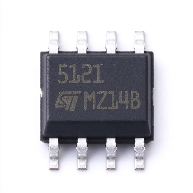
The STMicroelectronics TS393MD is a micropower dual CMOS voltage comparator with two independent comparison channels, open-drain outputs, and an 8-pin SOIC package. Each channel consumes 9 uA typically, has a typical input impedance of 10^12 ohm, and provides a typical response time of 2.5 us. The device is designed for low-power sensing and control circuits requiring high input impedance. A voltage comparator is an analog integrated circuit that compares an input voltage against a reference voltage and changes its output state when the relationship between those voltages changes. Comparators are used within analog signal chains, embedded control systems, and power management equipment. The TS393 belongs to the comparator family, the amplifier and analog IC hierarchy, and ultimately the broader integrated-circuit and semiconductor categories. The TS393MD provides two CMOS comparator channels in one package, reducing component count in dual-threshold or dual-signal systems. Its open-drain outputs permit wired-AND behavior when suitable pull-up resistors are installed. High input impedance minimizes loading of the sensed source, while the 2.5 us typical response time supports applications that need meaningful response speed without the continuous power demand of a faster bipolar comparator. The 9 uA typical supply current per comparator makes the device suitable for battery-operated instruments, portable monitors, and low-power sensor interfaces. STMicroelectronics describes the TS393 as compatible with the bipolar LM393 architecture, which can simplify comparison with conventional dual-comparator designs. The manufacturer also offers the similar TS3702 as a push-pull-output alternative, although its output topology is not interchangeable with the TS393MD open-drain interface without circuit changes. Typical uses include battery-powered threshold detection, sensor signal conditioning, industrial control inputs, and low-power monitoring systems. In each case, the two channels can monitor independent quantities or provide complementary decisions around a reference voltage. The TS393MD is also suitable where the source impedance is high and the comparator should avoid materially loading the monitored node. Designers should account for the open-drain output when selecting pull-up voltage and resistance. Input common-mode limits, supply-voltage range, offset behavior over temperature, and output sink-current capability must be checked in the manufacturer datasheet before finalizing a circuit. PCB placement should keep the comparator input paths short and away from high-current switching nodes to reduce noise coupling. This page combines the manufacturer device description, distributor package information, practical application guidance, and verified drop-in replacement information. It also identifies the measurable differences among directly compatible SOIC-8 options, helping engineers compare output type, supply current, temperature range, and qualification requirements before making a board-level replacement.

Запрос цены Контакты
TS393MDT - Micropower Dual Comparator | STMicroelectronics
TS393MDT

TS393MDT - Micropower Dual Comparator | STMicroelectronics

The STMicroelectronics TS393MDT is a micropower dual CMOS voltage comparator with two independent comparison channels, typically consuming 9 µA per comparator. The device accepts supply voltages up to 18 V, provides an input impedance of 10^12 Ω typical, and achieves a typical response time of 2.5 µs. It is packaged for surface-mount assembly in an 8-pin SOIC package, with the MDT ordering code identifying STMicroelectronics’ temperature-grade and delivery configuration. A voltage comparator is an analog integrated circuit that compares an input voltage against a reference voltage and changes its output state when the relationship between them changes. The TS393MDT belongs to the comparator hierarchy within amplifier and signal-conditioning integrated circuits. Its dual-channel architecture allows two independent threshold decisions in one package, while its CMOS input stage provides very high impedance and draws minimal supply current for battery-powered and always-on equipment. Key features include open-drain outputs, which permit wired-OR connection and operation with external pull-up resistors. The manufacturer describes the TS393 as compatible with the bipolar LM393 function while consuming approximately 20 times less current than the dual bipolar LM393. Its operating temperature range extends from -55 °C to 125 °C, making it suitable for industrial, automotive, and defense-related equipment when the complete system design and qualification requirements are satisfied. The electrical characteristics support threshold sensing where low supply current, high input impedance, and moderate propagation speed are more important than nanosecond response. A 10^12 Ω typical input impedance minimizes loading of high-impedance sensor nodes, while the 2.5 µs typical response time allows the device to respond to slowly changing or moderate-frequency events. The open-drain architecture requires a pull-up resistor when a logic-high output is required, and careful attention should be paid to output-node capacitance, leakage, and pull-up resistor selection. Typical applications include battery-powered monitoring circuits, industrial sensor interfaces, dual-threshold detection, window comparators, overvoltage and undervoltage supervision, and logic-level conversion between open-drain nodes. Two comparators in one package are especially useful when a compact design must monitor one signal against two limits or perform complementary decisions. When laying out a board, place input and pull-up components close to the relevant pins, maintain a stable ground reference, and avoid long traces around high-impedance input nodes. Because the output is open drain, the effective rise time depends on the pull-up resistance and total output capacitance rather than solely on the comparator’s internal response time. This product page combines the TS393MDT electrical characteristics, practical comparator design guidance, sourcing information, and a clearly qualified drop-in comparison with the bipolar LM393DT. It supports faster component selection by separating verified device facts from application-specific design considerations and replacement trade-offs.

Запрос цены Контакты
TS3A27518ERTWR - 6-Ch 2:1 Analog Mux, 240MHz | Texas Instruments
TS3A27518ERTWR

TS3A27518ERTWR - 6-Ch 2:1 Analog Mux, 240MHz | Texas Instruments

The Texas Instruments TS3A27518ERTWR is a bidirectional 6-channel 1:2 (SPDT) analog multiplexer/demultiplexer with 6.2 ohm on-resistance, 240 MHz bandwidth, and integrated IEC 61000-4-2 ESD protection, housed in a 24-pin WQFN (4x4 mm) package operating from a 1.65 V to 3.6 V single supply. An analog multiplexer is a signal-routing semiconductor that selects one of several input channels and connects it to a common output, functioning as a digitally controlled switch for both analog and digital signals. Within the signal-chain hierarchy, it sits between passive switches and full crosspoint matrices, and belongs to the broader family of interface and analog switch ICs used in power management and signal conditioning subsystems. Key features include low 6.2 ohm typical on-resistance for minimal signal attenuation, 21.5 pF typical switch capacitance, up to 240 MHz bandwidth for high-speed rail-to-rail signal handling, and -62 dB crosstalk and OFF isolation. The device also provides isolation in power-down mode (VCC = 0 V), and 1.8 V logic-threshold-compatible control inputs that allow direct interfacing with low-voltage microcontrollers. Architecturally, the TS3A27518E uses two control pins, each simultaneously controlling three 1:2 multiplexer sections, plus an enable pin that places all outputs in high-impedance mode. Integrated ESD cells rated to IEC 61000-4-2 on the signal pins eliminate the need for external TVS diodes in USB and port-protection designs, and the device is qualified for automotive applications. Typical applications include USB 2.0 high-speed signal switching, audio jack and headset detection, battery-powered portable equipment, and general-purpose analog signal routing in industrial systems. A key design consideration is on-resistance flatness across the signal range: at lower VCC the Ron rises, so budget for insertion loss at 1.65 V operation, and keep stub lengths short to preserve the 240 MHz bandwidth. This page adds value beyond the datasheet by synthesizing distributor pricing tiers, drop-in alternatives, cross-reference data, and practical design notes in one reference.

Запрос цены Контакты
TS3A44159RGTR - 0.45Ω Quad SPDT Analog Switch | TI
TS3A44159RGTR

TS3A44159RGTR - 0.45Ω Quad SPDT Analog Switch | TI

The Texas Instruments TS3A44159RGTR is a 0.45-Ω quad-channel single-pole double-throw (SPDT) analog switch housed in a 16-pin VQFN (RGT) 3x3 mm package. Operating from 1.65 V to 4.3 V, it delivers low on-state resistance with excellent Ron matching across four independent 2:1 multiplexers and supports bidirectional signal flow on every channel. Two logic-level control inputs select between the NO/NC paths of all four switches simultaneously, simplifying firmware-driven signal routing. An analog switch is a solid-state semiconductor device that routes analog or digital signals between two or more terminals under the control of a logic-level signal. It belongs to the analog switch and multiplexer family, which sits inside the broader interface IC category of integrated circuits. Quad SPDT switches are commonly used to swap between two sources on four channels at once, an arrangement also called a 2-channel DPDT function in this device. Key features include 0.45 Ω typical on-state resistance, 50 pA typical switch leakage, break-before-make switching to prevent momentary channel cross-connection, and a -3 dB bandwidth greater than 35 MHz. The control inputs are 1.8 V logic-compatible, while supply operation extends from 1.65 V to 4.3 V. ESD protection on the switch pins exceeds 2000 V per the HBM model. Architecturally the part uses CMOS transmission gates with integrated charge-pump-derived well biasing, enabling low Ron and rail-to-rail signal swing on a single positive supply. Ron flatness is held tight across the input common-mode range, which preserves harmonic distortion performance in audio paths. The device draws only microamps of quiescent current, which is essential for battery-powered systems. Typical applications include portable audio routing between headphone jack and Bluetooth receiver, USB 2.0 high-speed signal switching, SPI/I²C bus multiplexing, smartphone audio codec path selection, and PDA or portable media player source switching. Industrial uses include 4-wire resistance measurement multiplexing and analog front-end signal routing. When designing with this part, ensure that the logic-high level on IN1/IN2 exceeds 0.85 x VDD and the logic-low is below 0.15 x VDD to guarantee full CMOS-level switching. Place 0.1 µF bypass capacitors within 5 mm of the VDD pin to keep digital control noise out of the analog path. This page synthesizes distributor pricing, drop-in same-family alternatives, and practical PCB layout guidance not found in the manufacturer datasheet alone.

Запрос цены Контакты
TS3A4741DCNR - 0.9Ω Dual SPST Analog Switch | TI SOT-23-8
TS3A4741DCNR

TS3A4741DCNR - 0.9Ω Dual SPST Analog Switch | TI SOT-23-8

The Texas Instruments TS3A4741DCNR is a 0.9 Ω low on-resistance, low-voltage, single-supply, dual single-pole single-throw (SPST) analog switch housed in an 8-pin SOT-23 (DCN) package. It integrates two independent normally open (NO) switches, each with a 1:1 (SPST) topology, designed for 1.8 V logic compatibility when operated from a single 3 V supply rail. What is an SPST analog switch? An SPST (Single-Pole Single-Throw) analog switch is a solid-state semiconductor device that routes analog signals by electrically connecting or isolating one signal path. The TS3A4741 belongs to the broader category of analog switches and multiplexers, a subfamily of interface ICs used for signal routing in mixed-signal and low-power systems. Compared with mechanical relays, analog switches offer far faster switching speeds, lower power, smaller PCB area, and no mechanical bounce, at the cost of lower absolute voltage and current handling. Key specifications include a 0.9 Ω typical on-resistance (Ron), 1.8 V CMOS-compatible digital logic inputs, rail-to-rail analog signal handling, very low quiescent current, and integrated ESD protection. The two switches operate completely independently, allowing them to be used as separate signal paths or as complementary paths in a single function. The device is fabricated in a CMOS process and supports fast switching speeds, low off-leakage current, and bidirectional analog signal flow. Its small SOT-23-8 footprint and 1.8 V logic compatibility make it well suited to portable and battery-powered designs. Typical applications include audio signal routing in portable devices, switching between two sensors in handheld instruments, power rail multiplexing in low-power systems, and general-purpose signal gating in test equipment and consumer electronics. When designing with the TS3A4741, ensure the analog signal stays within the supply rails to avoid distortion or excessive leakage, and add 0.1 µF decoupling close to VCC. For applications requiring normally closed (NC) switches, use the pin-compatible TS3A4742. This page synthesizes verified distributor pricing, same-brand and cross-brand drop-in alternatives, and practical design notes not found in the manufacturer datasheet.

Запрос цены Контакты
TS3A4751PWR - 0.9-Ohm Quad SPST Analog Switch | Texas Instruments
TS3A4751PWR

TS3A4751PWR - 0.9-Ohm Quad SPST Analog Switch | Texas Instruments

The Texas Instruments TS3A4751PWR is a bidirectional, 4-channel, normally-open (NO) single-pole single-throw (SPST) analog switch in a 14-pin TSSOP package. It operates from a single 1.6V to 3.6V supply, delivers a maximum on-state resistance of 0.9 ohm at a 3V supply, and handles rail-to-rail analog signals with fast switching speeds and very low quiescent power. An analog switch is an IC that routes or isolates analog signal paths under digital control. Within the signal-routing hierarchy, the TS3A4751 belongs to the SPST switch family, a subset of analog switches and multiplexers used in signal conditioning and power-management systems. Key features include 0.9-ohm maximum Ron at 3V (1.5-ohm maximum at 1.8V), Ron flatness of 0.4-ohm maximum at 3V, and Ron matching of 0.05-ohm maximum at 3V. The 1.8-V CMOS-compatible digital inputs allow direct interface with low-voltage GPIO when using a 3-V supply, eliminating level-shift circuitry. The device is available in 14-pin TSSOP (PW), 14-pin VQFN (RGY), and 2x2-mm micro X2QFN (RUC) packages. The low Ron supports power-switching and low-distortion signal paths, while rail-to-rail operation preserves full signal swing on 1.8V, 2.5V, and 3.3V rails. Typical applications include low-voltage power switching, audio signal routing in portable devices, battery-powered test points, and general-purpose signal muxing in smartphones, tablets, and industrial sensing modules. Its normally-open configuration makes it suitable for fail-safe, default-disconnected paths. When designing, remember that Ron rises at lower supply voltages: at a 1.8-V supply the maximum Ron is 1.5 ohm, so account for insertion loss and on-resistance flatness in high-fidelity or precision-current paths. According to TI datasheet, the TS3A4751 is the NO-switch counterpart within the TI low-voltage quad SPST family.

Запрос цены Контакты
TS3A5018PWR - 10-Ohm Quad SPDT Analog Switch | Texas Instruments
TS3A5018PWR

TS3A5018PWR - 10-Ohm Quad SPDT Analog Switch | Texas Instruments

The Texas Instruments TS3A5018PWR is a quad single-pole double-throw (SPDT) analog switch designed to operate from a 1.8V to 3.6V supply in a 16-pin TSSOP (PW) package rated from -40C to +85C. It handles both digital and analog signals, and signals up to V+ can be transmitted in either direction. An analog switch is a semiconductor device that selectively connects or disconnects an analog signal path under digital control. It is a fundamental signal-routing building block in the broader family of multiplexers, demultiplexers, and interface ICs. Analog switches provide a low-resistance path when ON and a high-impedance path when OFF, replacing bulky mechanical relays in audio/video routing, data acquisition, and communication systems. Key features include the wide 1.8V to 3.6V operating range (ideal for battery-powered and 3.3V systems), low 10-ohm ON-state resistance with excellent channel-to-channel matching, and low charge injection that minimizes glitches during switch transitions. All four SPDT switches share a common enable function so the entire device can be disabled to reduce power consumption. The TS3A5018 is built on TI CMOS process technology, providing low quiescent power dissipation and high reliability. Bidirectional signal flow means either of the two throw terminals can serve as the port, essential for multiplexing and demultiplexing on the same hardware. Turn-on and turn-off times are fast, supporting high-speed signal routing in data converters and communication interfaces. Typical applications include audio signal routing in portable devices, battery-powered data acquisition front ends, communication interface switching, and test equipment signal multiplexing. The low power consumption and wide supply range make it well suited for portable and industrial designs. Design consideration: the 10-ohm ON resistance introduces series attenuation in high-impedance circuits, so prefer low-impedance loads or buffer the switched node. Place a 0.1uF decoupling capacitor close to the V+ pin, and use the enable pin in battery designs to cut standby current when switching is idle.

Запрос цены Контакты
TS3A5018QPWRQ1 - 10-Ohm Quad SPDT Analog Switch | Texas Instruments
TS3A5018QPWRQ1

TS3A5018QPWRQ1 - 10-Ohm Quad SPDT Analog Switch | Texas Instruments

The Texas Instruments TS3A5018QPWRQ1 is an automotive-qualified (AEC-Q100) quad single-pole double-throw (SPDT) analog switch designed to operate from a 1.8V to 3.6V supply. Packaged in a 16-pin TSSOP (PW), it provides four independent SPDT switches with a low 10-ohm on-resistance, handling both digital and analog signals up to V+ in either direction. An analog switch (also called an analog multiplexer/demultiplexer or bidirectional switch IC) is a semiconductor device that routes analog or digital signals through a MOSFET transmission gate controlled by a digital select input. Analog switches sit within the broader signal-routing hierarchy: analog switch IC -> signal multiplexer -> interface and switching IC -> analog signal chain. They are fundamental building blocks wherever a processor must dynamically reconfigure signal paths without degrading signal integrity. Key features of the TS3A5018QPWRQ1 include the low 10-ohm typical on-resistance, wide 1.8V to 3.6V single-supply operation suited to battery-powered and low-voltage systems, full rail-to-rail signal handling, and break-before-make switching that prevents momentary shorting of signal sources. The Q1 suffix denotes AEC-Q100 qualification for automotive environments, with an extended operating temperature range supporting under-hood and body electronics applications. The device uses CMOS transmission-gate architecture, which keeps on-resistance relatively flat across the signal range and minimizes signal distortion for audio and data-routing tasks. Because signals up to V+ can pass in either direction, the switches work equally well for multiplexing and demultiplexing, such as sharing a codec between microphone and headset paths or switching antenna and test signals. Typical applications include automotive infotainment audio routing, battery-management cell-monitoring multiplexing, portable instrument signal switching, and general-purpose I/O expansion in industrial control boards. Design tip: minimize RON signal loss by keeping source impedance low, and always provide a solid V+ decoupling capacitor (0.1uF close to the pin). Remember that the analog signal range is limited to the 0V-to-V+ supply window; signals outside this range must be blocked or level-shifted.

Запрос цены Контакты
TS3L100D - 4-Channel 3.3V SPDT LAN Switch | Texas Instruments
TS3L100D

TS3L100D - 4-Channel 3.3V SPDT LAN Switch | Texas Instruments

Texas Instruments TS3L100D is a four-channel, 3.3 V SPDT wide-bandwidth LAN switch with low on-state resistance, supplied in a 16-pin SOIC package. It provides two independent 2:1 multiplexer or demultiplexer paths per channel and uses a common switch-enable input, making it suitable for routing Ethernet-class signals through a compact analog switch network. An SPDT switch is an analog switch that selects one of two signal paths from a common terminal. The TS3L100 belongs to the broader LAN-switch, analog-switch, multiplexer, interface-IC, and semiconductor hierarchy. Its four-channel architecture consolidates repetitive signal-routing functions while reducing the number of discrete switches required in networking, test, measurement, and embedded communication equipment. Key features include four independently addressed SPDT channels, a common switch-enable control, 3.3 V operation, wide signal bandwidth, and low on-state resistance. The on-state resistance is important because signal attenuation and insertion loss can increase as switch resistance rises. Wide bandwidth also makes the device useful when routing higher-frequency data or analog signals rather than only slow control signals. The TS3L100D combines multiplexing and demultiplexing in one device. It can route a common source toward either destination, or direct one of two inputs to a shared output, depending on the external connection and enable state. This dual-use architecture allows the same device to support shared test equipment, muxed signal paths, line monitoring, and compact network-interface routing. Typical applications include 10/100 Ethernet PHY signal routing, LAN interface multiplexing, test-and-measurement signal paths, instrumentation, network adapters, and embedded systems that require multiple high-speed connections. In Ethernet designs, the switch can reduce the number of discrete routing components while preserving a compact board footprint. PCB layout should keep input and output traces short, provide a solid ground reference, and decouple the 3.3 V supply near the device. Designers should consult the Texas Instruments pin-description table before routing signals because the exact enable polarity, channel pin mapping, and breakout configuration must match the intended PCB footprint. This product page consolidates the official device description, package information, sourcing guidance, application analysis, and verified-source links. It also distinguishes confirmed electrical characteristics from parameters that require confirmation from the manufacturer datasheet before schematic or layout release.

Запрос цены Контакты
TS3L110D - 4-Channel 10/100 LAN Switch | Texas Instruments
TS3L110D

TS3L110D - 4-Channel 10/100 LAN Switch | Texas Instruments

The Texas Instruments TS3L110D is a 3.3 V, 2:1 SPDT, four-channel 10/100 Base-T LAN switch with eight differential channels muxed to four channels. It is packaged in a 16-pin SOIC and operates from 3 V to 3.6 V. The device provides an 8 ohm on-resistance, approximately 700 uA of supply current, and integrated control for selecting between paired differential LAN signals. An Ethernet LAN switch is an interface integrated circuit that routes differential signals between a transceiver or controller and multiple physical network connections. The TS3L110D belongs to the broader networking-switch hierarchy: four-channel LAN switch, special-purpose interface IC, and semiconductor. Its 2:1 multiplexer arrangement allows one differential signal pair to be connected to either of two alternatives, reducing the number of external routing components required in compact Ethernet equipment. The TS3L110D supports four independently controlled 10/100 Base-T channels, with each channel implemented as an SPDT selector. Its 3 V to 3.6 V supply range is suited to 3.3 V systems, while the 8 ohm on-resistance provides a defined insertion-loss contribution at Ethernet signal rates. A low supply current of approximately 700 uA is useful in power-constrained network-access equipment. The 16-pin SOIC package supports conventional surface-mount assembly and inspection. The device multiplexes eight differential inputs to four output channels. This arrangement is appropriate when an Ethernet controller, media-access controller, or PHY interface needs selectable access to more than one physical channel. Because it is a switching device rather than an active repeater or transceiver, the TS3L110D does not itself establish the physical-layer link. It selects existing differential signals and must be paired with suitable 10/100 Ethernet PHYs, magnetics, connectors, and network-control circuitry. Typical uses include compact Ethernet switches, network interface controllers, industrial Ethernet equipment, embedded gateways, and set-top or communications products. The part can also be used in test systems where a controller must route differential pairs between instrumentation or PHY channels. Design choices should account for trace impedance, connector and magnetics layout, control timing, and the high-speed return path between the switch and its Ethernet PHY. Use the manufacturer pin-description and typical-application diagrams when assigning control inputs and differential nets. Maintain controlled-impedance routing for Ethernet pairs, keep switch traces short, and place bypass capacitance close to the supply pin. Verify the exact enable polarity, control interface, and recommended resistor and capacitor values against the current manufacturer datasheet before releasing a PCB. This page organizes the verified 3.3 V supply, SPDT configuration, four-channel architecture, 8 ohm on-resistance, approximately 700 uA supply current, 16-pin SOIC construction, application guidance, and qualified replacement options into an engineering-focused reference.

Запрос цены Контакты
TS3USB3000MRSER - DPDT USB 2.0/MHL Switch | TI | UQFN-10
TS3USB3000MRSER

TS3USB3000MRSER - DPDT USB 2.0/MHL Switch | TI | UQFN-10

The Texas Instruments TS3USB3000MRSER is a double-pole, double-throw (DPDT) analog switch that combines a USB 2.0 High-Speed (480 Mbps) switch and a Mobile High-Definition Link (MHL) switch in a single 10-pin UQFN (RSE) package measuring 1.5 mm × 2.0 mm. It supports a -3 dB bandwidth of 6.1 GHz on the MHL path and operates from a 2.3 V to 4.8 V supply. The device is designed to share a common USB or Micro-USB connector between USB 2.0 data and MHL video signals in mobile phones, tablets, and portable media devices. A USB switch IC is a special-purpose analog multiplexer that routes high-speed differential signals between a single downstream port and two upstream paths (host vs. MHL sink). In the hierarchy of power management and signal routing components, this part belongs to the USB interface IC category, sitting between the connector and the application processor. DPDT switches such as the TS3USB3000 are critical because they must pass 480 Mbps USB signals and up to 3 GHz MHL content with minimal insertion loss, low crosstalk, and high off-isolation. Key features of the TS3USB3000 include low on-resistance (Ron) on the USB data paths, low on-capacitance (Con) for high-bandwidth signal transmission, 1.8-V-compatible select pins for direct GPIO control from a mobile processor, and a quiescent current of approximately 5 uA. The wide supply range (2.3 V to 4.8 V) covers both 3.3 V system rails and the typical 3.8 V Li-ion battery range without additional regulation. The small 1.5 mm × 2 mm UQFN footprint makes it ideal for space-constrained mobile applications. The TS3USB3000 uses a charge-pump-less architecture with simple CMOS logic-level select inputs. The two select pins (S1 and S0 per TI documentation) determine whether the common port is routed to the USB path or the MHL path. Internal ESD protection on the signal pins improves robustness against connector-level transients, which is critical for hot-plug consumer electronics. Typical applications include smartphones and tablets with MHL-enabled video output, automotive infotainment systems that mirror mobile content via USB or MHL, portable media players, and USB/MHL dongles. The wide bandwidth also makes it suitable for any system needing to multiplex two high-speed differential pairs onto a single connector. When designing with this part, place the device as close as possible to the USB/MHL connector to minimize stub lengths and signal-integrity degradation. Use controlled-impedance differential routing (90 ohm) on both sides of the switch, and provide adequate ground stitching vias along the signal path to maintain return-current continuity. This page synthesizes distributor pricing, pin-compatible alternatives, and practical design notes that are not aggregated in any single manufacturer datasheet or distributor catalog page.

Запрос цены Контакты
TS3V330D - 4-Channel SPDT Video Switch | Texas Instruments
TS3V330D

TS3V330D - 4-Channel SPDT Video Switch | Texas Instruments

Texas Instruments TS3V330D is a 3.3 V, four-channel, 2:1 SPDT video switch packaged in a 16-pin SOIC. It provides one enable input for the quad switch and is designed for wide-bandwidth video-routing applications. The device operates across the -40°C to +85°C industrial temperature range. Its low on-state resistance is intended to minimize signal attenuation when a video path is selected. A video switch is an analog multiplexer or demultiplexer that routes one of two signal paths to a common output. The SPDT configuration supports source selection, signal swapping, and isolation between alternate inputs. In the system hierarchy, the TS3V330D belongs to the analog switch family, which falls under interface ICs and broader semiconductor signal-routing devices. Four integrated channels reduce component count when several video lines must be switched together. The principal features of the TS3V330D include four independent 2:1 switch channels, a common single switch-enable input, a 3.3 V supply requirement, wide-bandwidth video switching, and low on-state resistance. The 16-SOIC package supports conventional surface-mount assembly. These characteristics make the device relevant to video test equipment, multimedia routing, projection systems, display processing, and industrial imaging designs where multiple source paths must be selected electronically. The TS3V330D uses a single enable-control architecture rather than four separate control inputs. This simplifies command-line interfacing when all four channels must change state together. Its wide-bandwidth design is intended to preserve video signals while keeping conduction loss relatively low. Because a video switch is an analog device, signal integrity depends not only on on-state resistance but also on off-state isolation, channel matching, board-level parasitics, and the impedance of the source and destination circuitry. Typical implementations include selecting between composite or component video inputs, routing test signals into an oscilloscope or video analyzer, switching cameras within surveillance equipment, and controlling auxiliary video paths in projection or display equipment. The common enable input also supports systems that need to mute or disconnect several video lines together. Firmware-controlled source selection is particularly practical when the same board must support several external connectors. PCB layout should keep video traces short, provide a continuous ground reference, and place bypass capacitance close to the supply pin. Designers should verify the complete channel bandwidth, isolation, insertion loss, and crosstalk against the source impedance and cable length. The common enable signal should be controlled only after the selected input is stable, preventing transient switching artifacts from reaching downstream video circuitry. This product page combines the device identity, package information, operating limits, confirmed cross-reference options, and practical design guidance for engineers evaluating the TS3V330D. It also distinguishes the core four-channel SPDT switching function from broader interface and signal-routing categories, making the component easier to compare with suitable video-switching designs.

Запрос цены Контакты
TS3V340D - Quad SPDT 3.3V Video Switch | Texas Instruments
TS3V340D

TS3V340D - Quad SPDT 3.3V Video Switch | Texas Instruments

The Texas Instruments TS3V340D is a 3.3 V, four-channel video switch with four independent 2:1 SPDT switch functions, low and flat on-state resistance, and high-bandwidth signal routing in a 16-pin SOIC package. It is designed for compact systems that require controlled selection between two video signals for each of four channels. An analog video switch is an interface IC that routes high-frequency baseband video signals between a common output and one of two selectable inputs. Its switching architecture allows a source to be connected to a display, processing chain, test point, or other destination without duplicating the upstream signal source. The TS3V340 family combines video-signal switching with a 3.3 V supply, making it appropriate for modern low-voltage display and video-processing equipment. The principal features of the TS3V340D include four switch channels, a 2:1 SPDT configuration per channel, low and flat on-state resistance, and high-bandwidth operation. The flat resistance characteristic helps reduce signal-level variation as the switch state changes. Its 16-pin SOIC package supports conventional surface-mount assembly while keeping the four-channel routing function in a relatively compact footprint. Each independently controlled SPDT channel can connect its common terminal to either of two input terminals. This arrangement is useful for source selection, signal-path isolation, video test points, and routing between primary and backup signal paths. The manufacturer describes the TS3V340 as a 3.3 V, four-channel video switch with flat on-state resistance, while the TS3V340D ordering option is associated with the 16-pin SOIC package. Typical uses include projector input selection, video observation systems, industrial inspection equipment, broadcast and presentation infrastructure, test and measurement systems, and consumer displays. Multiple switch channels can support several connections within one compact assembly, reducing the number of discrete routing components required on a video-oriented circuit board. For implementation, route high-speed video traces as short and directly connected as practical, maintain a continuous ground reference beneath the signal path, and place the device close to the switching point. Control inputs should be driven from compatible 3.3 V logic, and unused inputs should be configured according to the manufacturer pin-description table. Verify timing, signal levels, and channel isolation in the final board environment. This product summary combines the manufacturer device description with application-oriented guidance, package information, engineering cautions, and transparent sourcing information. It is intended to help designers evaluate the TS3V340D for 3.3 V video-routing tasks while separately checking the authoritative datasheet for complete electrical limits, timing, and pin assignments.

Запрос цены Контакты
TS507CD - 1.9MHz Precision Rail-to-Rail Op Amp | STMicroelectronics
TS507CD

TS507CD - 1.9MHz Precision Rail-to-Rail Op Amp | STMicroelectronics

The STMicroelectronics TS507CD is a single-circuit, high-precision operational amplifier with rail-to-rail input and output operation, a 1.9 MHz gain-bandwidth product, and an 8-SOIC package. It is designed for general-purpose precision signal conditioning and supports stable operation across its supply-voltage range. An operational amplifier is a voltage-feedback amplifier used to amplify, buffer, filter, or compare small analog signals. The TS507 belongs to the operational-amplifier hierarchy within analog ICs and broader semiconductor signal-conditioning systems. Its rail-to-rail input stage accepts signals close to the supply rails, while the rail-to-rail output stage provides useful output swing near both limits. The TS507CD uses precision trimming to achieve low input-offset voltage without external zeroing. Its listed maximum input-offset voltage is 550 µV, and its typical common-mode rejection ratio is 115 dB. A 1.9 MHz gain-bandwidth product supports general-purpose closed-loop operation, while the low 850 µA supply current suits low-power analog systems. The device is specified as a single general-purpose amplifier in an 8-SOIC package. Its operating temperature range is listed as 0°C to 85°C, and its typical output-current capability is 128 mA. These characteristics make it appropriate for precision sensor interfaces, active filters, signal buffers, and portable equipment where low offset and low supply current are more important than high bandwidth. Typical uses include bridge-sensor amplification, transducer-signal conditioning, low-frequency active filters, and buffered analog measurements. Because the amplifier operates rail-to-rail at the input and output, system designers can use more of the available supply range, but common-mode and output-swing limits still require verification under the intended load and supply conditions. When laying out a TS507CD circuit, keep feedback components and the input source connections short, and route high-impedance inputs away from switching nodes. Decoupling capacitors should be placed close to the supply and ground pins. Confirm gain-bandwidth, output-swing, and stability requirements against the actual gain, load, supply voltage, and operating temperature. This page combines the TS507CD device description, package information, application guidance, comparison parameters, and verified sourcing references to help engineers evaluate the amplifier and identify technically suitable alternatives before PCB release.

Запрос цены Контакты
TS507ID - Low-Offset Rail-to-Rail Op Amp | STMicroelectronics
TS507ID

TS507ID - Low-Offset Rail-to-Rail Op Amp | STMicroelectronics

The STMicroelectronics TS507ID is a single-circuit, general-purpose operational amplifier in an 8-pin SOIC package. It is designed around rail-to-rail input and output operation, allowing the amplifier to operate close to the supply rails in precision analog signal chains. The TS507 uses a new trimming technique that produces very low offset voltage without requiring external zeroing, reducing assembly time and eliminating the need for a trim potentiometer in precision measurement circuits. A rail-to-rail operational amplifier is an amplifier whose input common-mode range and output swing extend close to both supply-voltage limits. This capability is valuable when the signal being amplified operates near a positive or negative rail and a conventional amplifier would saturate. The TS507 therefore suits precision instrumentation, sensor interfaces, low-level signal conditioning, and measurement systems where usable signal range is more important than absolute isolation from the rails. The TS507ID is identified by DigiKey and Mouser as a standard, general-purpose instrumentation amplifier section in an 8-SOIC package. Its trimmed internal design targets stable electrical characteristics across the operating range and very low offset without external adjustment. For designs requiring tighter control of input bias current, offset drift, noise, bandwidth, supply current, or temperature range, consult the manufacturer datasheet and select the appropriate TS507 grade and package variant. Because the TS507ID accepts both positive and negative signal inputs and supports near-rail output swing, it can serve as the active element in difference amplifiers, current-to-voltage converters, bridge-sensor front ends, and precision feedback networks. The 8-pin SOIC footprint also allows it to be placed in the same general layout class as many standard single op amps, although engineers should verify the actual pin assignment and stability requirements before substituting another device. When designing with the TS507ID, begin by defining the signal amplitude, common-mode range, required output swing, source impedance, and noise gain. Check the datasheet for the operating voltage range, unity-gain bandwidth, slew rate, input bias current, offset voltage, noise density, and stability conditions. Place the feedback components close to the amplifier, keep sensitive input nodes away from switching-current paths, and use a ground layout that minimizes voltage drops across analog return currents. This page combines manufacturer-level product information, verified distributor listings, package and pin-assignment guidance, application analysis, and drop-in replacement guidance. It also distinguishes confirmed package-compatible TS507 family variants from options that require additional electrical verification, helping engineers narrow a redesign quickly before committing a new component to a PCB.

Запрос цены Контакты
TS512ID - 3 MHz Precision Dual Op Amp | STMicroelectronics
TS512ID

TS512ID - 3 MHz Precision Dual Op Amp | STMicroelectronics

The STMicroelectronics TS512ID is a precision dual operational amplifier with two independent amplifiers, a 3 MHz gain-bandwidth product, and a maximum input offset voltage of 500 µV. The device is supplied in an 8-pin SOIC package and operates from single or dual power supplies, making it suitable for signal-conditioning and instrumentation applications requiring two amplifiers in one package. An operational amplifier is an analog integrated circuit that uses very high open-loop gain to amplify the difference between its inverting and non-inverting inputs. Precision operational amplifiers are a subtype of voltage-feedback amplifiers characterized by low offset voltage, low distortion, low noise, and stable operation with feedback. The dual-amplifier configuration places two amplifiers in one package, reducing board area and simplifying paired signal-processing circuits. The TS512 family provides a 3 MHz gain-bandwidth product, low input offset voltage of 500 µV maximum, low power consumption, short-circuit protection, low distortion, low noise, high channel separation, and internal ESD protection. According to the STMicroelectronics family datasheet, the minimum slew rate is 0.8 V/µs for TS512 and TS512A. The related TS512B has a guaranteed higher minimum slew rate of 1.072 V/µs. The TS512 family uses internal frequency and phase compensation to support stable operation in voltage-follower configurations. This is useful in application circuits where one amplifier buffers a source and the other performs gain or filtering. Its dual supply range is ±1.5 V to ±15 V, while single-supply operation is supported from 3 V to 30 V, allowing use in both conventional analog circuits and higher-voltage industrial interfaces. Typical uses include sensor-signal conditioning, low-level instrumentation, active filtering, audio preamplification, and general analog signal processing. The dual channel can implement matched buffer, gain, summing, or differential stages. Because offset voltage influences accuracy near the zero-voltage operating point, input-source resistance and bias-current compensation should be evaluated carefully. PCB layout should keep input and feedback paths short and place input compensation or filtering components close to the relevant amplifier pins. Both channels should share stable supply decoupling, while avoiding current paths through analog ground that carry output or digital return current. The SOIC package is suitable for conventional surface-mount assembly and conventional thermal design at low to moderate output current. This page consolidates the verified manufacturer-family information, distributor listing details, package data, sourcing information, and engineering guidance for TS512ID. It distinguishes documented TS512-family characteristics from unavailable detailed electrical limits and clearly identifies uncertainty where the supplied source data does not provide a defensible value.

USD $0,43 В наличии
TS512IDT - 3MHz Dual Precision Op Amp | STMicroelectronics
TS512IDT

TS512IDT - 3MHz Dual Precision Op Amp | STMicroelectronics

STMicroelectronics TS512IDT is a dual precision operational amplifier with a 3 MHz gain-bandwidth product, 8 nV/√Hz input-voltage noise density, and 0.03% distortion, housed in an 8-pin SOIC package. The TS512x family combines internally compensated low-noise operation with stable voltage-follower performance, making each amplifier suitable for precision signal conditioning and audio paths. An operational amplifier, or op amp, is a high-gain differential amplifier that uses external feedback to set gain and filtering behavior. In the electronics hierarchy, the TS512IDT is a precision operational amplifier within the broader amplifier IC and analog signal-processing categories. Its two independent channels allow one package to process two signals, while internal frequency and phase compensation simplify voltage-follower and other high-gain configurations without external compensation components. The principal features include 3 MHz gain-bandwidth product, 8 nV/√Hz noise density, 0.03% distortion, low power consumption, short-circuit protection, and high channel separation. Operation from a single 3 V to 30 V supply or from dual ±1.5 V to ±15 V rails gives designers flexibility across industrial, instrumentation, and signal-conditioning systems. The low-noise and low-distortion characteristics are particularly relevant when small sensor and audio signals must be amplified without adding substantial broadband noise or harmonic distortion. Internally compensated architecture supports stable operation in voltage-follower configurations despite the amplifier's relatively high gain-bandwidth product. The TS512x family is designed for general-purpose precision applications where clean signal amplification matters more than very high speed. Two channels in one package reduce board-area requirements, while high channel separation helps maintain signal integrity when the channels process related low-level signals. The amplifier also includes ESD protection and a macromodel for circuit simulation. Typical uses include audio preamplification, instrumentation-amplifier input stages, active filters, sensor signal conditioning, transducers, and general-purpose analog measurement chains. The 8-pin SOIC package is useful where conventional surface-mount assembly is required and the circuit operates across the stated -40°C to +125°C temperature range. The wide supply-voltage range also permits operation from industrial rails while retaining compatibility with lower-voltage analog systems. Designers should verify input and output voltage limits, common-mode range, output-swing behavior, and stability against the exact load connected to each channel. Decoupling capacitors should be placed close to the supply pins, while sensitive-input routing should avoid nearby switching nodes and high-current return paths. The dual package does not require matched channels for general use, but input bias-current and offset behavior must be considered in precision DC measurements. This page combines the TS512IDT's principal electrical characteristics with pin-compatible family alternatives, application guidance, comparison parameters, and practical circuit-design notes. These engineering-focused details help shorten component evaluation and support a more reliable transition from initial schematic design through PCB implementation and production qualification.

Запрос цены Контакты
TS512IN - 3MHz Dual Precision Op Amp | STMicroelectronics
TS512IN

TS512IN - 3MHz Dual Precision Op Amp | STMicroelectronics

The STMicroelectronics TS512IN is a precision dual operational amplifier with a 3 MHz gain-bandwidth product, 1.5 V/µs slew rate, and a maximum input offset voltage of 500 µV, supplied in an 8-pin Mini DIP package. It is designed for general-purpose instrumentation, analog signal conditioning, and dual-channel measurement applications where two amplifiers share the same package. A dual operational amplifier is an analog integrated circuit containing two independent amplifier channels. Operational amplifiers are voltage amplifiers whose behavior depends mainly on external feedback components. The TS512IN combines frequency-compensated amplifiers for stable voltage-follower operation, low distortion, low noise, short-circuit protection, and internal ESD protection. The 3 MHz gain-bandwidth product supports useful closed-loop bandwidth well below 3 MHz at higher noise gains, while the 1.5 V/µs slew rate improves response to larger transient signals. A maximum offset voltage of 500 µV helps reduce DC error in precision feedback networks. Its dual-channel organization reduces package count and simplifies PCB routing when two amplified signals must be processed under shared supply conditions. The device operates from single 6 V to dual ±15 V supplies, matching conventional analog and industrial voltage ranges. Internal phase compensation allows voltage-follower use without an external compensation network. Short-circuit protection limits the effects of output overload, although sustained shorts still require appropriate supply and thermal checks. Internal ESD protection improves handling robustness without eliminating the need for normal assembly precautions. TS512IN applications include sensor-interface amplification, low-frequency instrumentation, dual audio-channel control, buffering, active filtering, and general analog signal conditioning. Designers should place input and feedback components close to their associated pins, observe the specified common-mode and output-current limits, and avoid excessive loading near the bandwidth and slew-rate limits. This product page combines verified manufacturer-linked specifications, source URLs, package information, application guidance, and honest comparison limitations. It distinguishes confirmed TS512IN attributes from parameters that require verification before a PCB or production cross-reference is approved.

Запрос цены Контакты
TS514ID - High-Speed Precision Quad Op Amp | STMicroelectronics
TS514ID

TS514ID - High-Speed Precision Quad Op Amp | STMicroelectronics

STMicroelectronics TS514ID is a high-speed, precision quad operational amplifier with four amplifier circuits, internally compensated frequency and phase response, short-circuit protection, internal ESD protection, and a 14-pin SOIC package. The verified product data identifies a maximum offset voltage of 500 uV and highlights a high gain-bandwidth product, low distortion, low noise, low power consumption, and high channel separation. The TS514ID is intended for instrumentation and general-purpose precision signal-processing designs requiring four amplifiers in one package. An operational amplifier, commonly called an op amp, is a voltage-controlled differential amplifier with very high open-loop gain. Its external feedback network determines the closed-loop behavior. The TS514 belongs to the operational-amplifier hierarchy, which includes instrumentation amplifiers, buffer amplifiers, comparators, and general-purpose voltage amplifiers. Internal phase compensation allows the TS514 to operate as a voltage follower despite its high gain-bandwidth product, reducing the external compensation effort required in many designs. The quad architecture integrates four amplifier channels into one 14-pin SOIC-14 package. Verified manufacturer-related product descriptions identify low offset voltage, low power consumption, short-circuit protection, low distortion, low noise, high gain-bandwidth product, high channel separation, and internal ESD protection. These characteristics make the device applicable to precision buffering, signal conditioning, instrumentation, industrial measurement, and general analog signal-processing systems. Each amplifier requires stable supply decoupling and careful handling of output-current limits. The TS514 uses internal frequency and phase compensation. This architecture is particularly useful in follower and precision-gain configurations because the compensation is already incorporated into the device. Its high speed does not eliminate the need for short feedback traces, adequate grounding, and supply bypassing. Designers should avoid long output routing and place input, output, and ground returns so that parasitic capacitance does not degrade stability or transient response. Typical uses include four-channel sensor conditioning, low-level signal amplification, active filtering, voltage buffering, and instrumentation chains requiring several matched amplifier functions. Industrial control and test equipment can also use the quad package to reduce board area compared with four discrete single-amplifier packages. Where precision offset and noise dominate, the complete manufacturer datasheet should be consulted for test conditions and application-specific limits. The principal design trade-off is speed versus power and stability margin. Although the TS514 supports high-speed operation and voltage-follower use, board layout, capacitive loading, output-current demand, and supply bypassing remain critical. A short, low-inductance layout with local decoupling is recommended. Application notes and the manufacturer datasheet should control the final compensation, grounding, and thermal implementation. This product page combines verified distributor and datasheet information with practical guidance on precision analog design, package reuse, selection criteria, and drop-in alternatives. It also distinguishes confirmed TS514-family candidates from cross-package or merely functional substitutes so engineers can avoid redesigns that require PCB changes.

Запрос цены Контакты
TS514IN - Quad Precision Op Amp | STMicroelectronics | DIP-14
TS514IN

TS514IN - Quad Precision Op Amp | STMicroelectronics | DIP-14

The STMicroelectronics TS514IN is a high-performance quad operational amplifier with internal frequency and phase compensation, supplied in a 14-DIP package. The device contains four amplifier channels in one package and is designed for general-purpose instrumentation, signal-conditioning, and analog control applications where stable voltage-follower operation is useful. The verified manufacturer description identifies low offset voltage, low power consumption, short-circuit protection, low distortion, low noise, high gain-bandwidth product, high channel separation, and internal ESD protection as key features. An operational amplifier is an analog integrated circuit that amplifies the voltage difference between its inverting and non-inverting inputs. A quad operational amplifier extends this architecture to four independent channels in one package, reducing board area and simplifying multi-channel designs. The TS514IN belongs to the broader operational-amplifier, analog-amplifier, signal-conditioning, and semiconductor hierarchy. The TS514IN's compensated architecture is intended to support stable operation as a voltage follower despite its high gain-bandwidth product. Internal compensation simplifies circuit design when unity-gain stability is required, while short-circuit protection improves robustness in conventional analog signal paths. Low offset voltage supports precision-oriented instrumentation, and low noise and low distortion are useful for audio and measurement front ends. Four channels make the device suitable for sensor signal conditioning, current-voltage conversion, active filtering, waveform shaping, instrumentation amplifiers, feedback networks, and general analog control loops. The 14-DIP package is appropriate for through-hole prototyping, educational systems, laboratory instruments, and industrial assemblies where a dual-inline footprint is preferred over a fine-pitch surface-mount package. The principal design consideration is to verify the supply-voltage limits, input common-mode range, output swing, input bias current, noise density, and load-current behavior against the manufacturer datasheet before finalizing a new design. Decoupling capacitors should be placed close to the supply pins, and unused amplifier inputs should be tied to a defined voltage within the input common-mode range. This page consolidates the verified manufacturer and distributor information, package details, application guidance, technical limitations, and drop-in replacement analysis. It also identifies parameters that require confirmation from the complete TS514 datasheet rather than substituting unverified assumptions.

Запрос цены Контакты
TS522ID - Dual 15MHz Low-Noise Op Amp | STMicroelectronics
TS522ID

TS522ID - Dual 15MHz Low-Noise Op Amp | STMicroelectronics

The STMicroelectronics TS522ID is a monolithic dual operational amplifier optimized for precision audio signal processing. It provides two amplifiers, a 15 MHz gain-bandwidth product, a 7 V/µs slew rate, low-voltage noise of 4.5 nV/√Hz, and a maximum input offset voltage of 850 µV in an 8-pin SOIC package. The device operates from 5 V to 30 V over an industrial temperature range of -40°C to +125°C. An operational amplifier is a voltage-controlled differential amplifier that uses feedback to amplify the difference between two input voltages. The dual configuration places two amplifiers in one package, allowing stereo audio, balanced signal paths, active filtering, or independent measurement channels to share a common footprint. Within the broader semiconductor hierarchy, the TS522 belongs to the operational-amplifier family, the analog amplifier category, and the signal-conditioning IC hierarchy. The TS522 combines low input offset, low voltage noise, and high dynamic performance for audio-oriented designs. Its 850 µV maximum input offset voltage supports accurate signal amplification, while the 4.5 nV/√Hz voltage-noise density is particularly relevant when processing low-level microphone, musical-instrument, or line-level signals. A 15 MHz gain-bandwidth product provides useful bandwidth for audio and general-purpose precision applications, and the 7 V/µs slew rate improves large-signal response. Internally, each amplifier is configured around high-gain stages with internal ESD protection. The manufacturer datasheet reports low distortion of 0.002%, macromodel inclusion, and excellent frequency stability. These characteristics make the TS522 suitable for precision audio signal chains where low noise, low distortion, and predictable frequency response matter more than very low power consumption. Typical uses include stereo audio preamplification, active crossover filters, mixer input stages, microphone preamplifiers, audio buffer circuits, and low-level sensor-conditioning channels. Two amplifiers in the same 8-pin SOIC package can reduce board area in stereo designs, while the industrial temperature range supports industrial control, communications, and instrumentation equipment. Designers should verify the required supply headroom, input common-mode range, output swing, noise gain, and stability for the selected feedback network. Decoupling capacitors should be placed close to the supply pins, and sensitive audio inputs should use short traces with suitable grounding to minimize parasitic pickup. A SPICE macromodel is available for circuit simulation, but board-level stability and distortion should still be verified with real components. This page consolidates the verified TS522ID operating characteristics, sourcing links, application guidance, design cautions, and replacement information. It also distinguishes confirmed technical facts from parameters that were not present in the supplied source data, helping engineers make a defensible design decision without treating unverified values as guaranteed specifications.

Запрос цены Контакты
TS522IDT - 15MHz Dual Low-Noise Op Amp | STMicroelectronics
TS522IDT

TS522IDT - 15MHz Dual Low-Noise Op Amp | STMicroelectronics

STMicroelectronics TS522IDT is a dual precision operational amplifier with a 15 MHz gain-bandwidth product, 4.5 nV/√Hz low-voltage noise, and a 7 V/µs slew rate. The device operates from 2.5 V to 15 V and is packaged in an 8-pin SOIC for dual-amplifier signal-conditioning applications. An operational amplifier is a voltage-controlled, high-gain analog building block that compares an input signal with a feedback-defined reference. The TS522IDT contains two amplifiers in one package, placing it within the operational-amplifier hierarchy of analog ICs and broader semiconductor signal-processing components. Its dual configuration reduces package count when a board requires two closely related analog channels. The primary benefits are low input offset voltage, low voltage noise, and high dynamic performance. A 4.5 nV/√Hz noise density supports accurate amplification of small signals, while the 15 MHz gain-bandwidth product provides useful bandwidth for audio, instrumentation, filtering, and general-purpose analog stages. The 7 V/µs slew rate allows the amplifiers to follow changing signals with limited distortion. Each amplifier can operate with supply voltages between 2.5 V and 15 V, allowing operation from low-voltage analog systems through higher-voltage industrial analog rails. The monolithic dual-amplifier construction is intended to provide matching behavior between the two channels, although circuit-level offset and noise measurements should still be checked in the final design. The 8-pin SOIC package supports conventional surface-mount assembly and is convenient for prototypes as well as production boards. Typical uses include low-noise audio preamplification, microphone signal conditioning, active filtering, instrumentation amplifiers, sensor interfaces, and analog buffering. Two independent amplifier channels can process stereo audio, implement a differential input stage, or combine filtering with output buffering. Supply-headroom planning remains important because the usable output range depends on the selected rail voltages and output load. For low-noise layouts, use short feedback paths, keep input and ground connections away from switching nodes, and place input bypass capacitance close to the supply pins. Decoupling requirements and compensation limits should be confirmed in the STMicroelectronics TS522IDT datasheet. Stable operation also depends on following the prescribed capacitive-load limits and providing suitable output-current margin for the connected load. This product page combines the verified TS522IDT specifications, package information, replacement considerations, comparison parameters, and application guidance. It is intended to help engineers determine whether the dual amplifier fits a specific voltage, bandwidth, noise, and PCB-layout requirement before completing a prototype or production design.

Запрос цены Контакты