Товары (38.000+)

BUF634FKTTT - 250mA 180MHz High-Speed Buffer | TI
BUF634FKTTT

BUF634FKTTT - 250mA 180MHz High-Speed Buffer | TI

The Texas Instruments BUF634FKTTT is a 250 mA high-speed unity-gain open-loop buffer amplifier with 180 MHz bandwidth and 2000 V/us slew rate, housed in a 5-pin TO-263 (DDPAK/KTT) package rated from -40C to +125C. A buffer amplifier is a unity-gain analog stage whose sole purpose is to provide current drive and isolation between a high-impedance source and a low-impedance load. In the power-management and signal-chain hierarchy, buffers sit between precision op amps and their loads, preventing the output stage of the amplifier from dissipating load current internally - a phenomenon known as thermal feedback that degrades offset and drift specifications. The defining feature of the BUF634 is its ability to operate inside the feedback loop of an op amp to multiply available output current up to 250 mA, eliminate thermal feedback, and dramatically improve capacitive load drive. Its 2000 V/us slew rate and 180 MHz bandwidth preserve the speed of the host amplifier, while the wide supply range of +/-2.25V to +/-18V (4.5V to 36V total) covers virtually all precision analog rails. Internally, the BUF634 is a complementary class-AB emitter-follower architecture with a bandwidth-select pin (BW). Tying BW to V- engages the full 180 MHz / 10 mA-standby mode; leaving BW open reduces quiescent current for power-sensitive designs at reduced bandwidth. The KTT DDPAK-5 tab provides a low-thermal-resistance path to the PCB copper for sustained 250 mA output currents. Typical applications include output-current boosting of precision op amps in test and measurement front ends, cable and capacitive-load drivers in data acquisition systems, video and IF signal distribution, and loop-powered actuator drivers in industrial control. Design consideration: place a small series resistor or short snubber at the output when driving long cables, and keep the BW pin connection as short as possible to avoid RF pickup in high-speed mode. This page synthesizes verified distributor data, the TI BUF634 family cross-reference, and practical design guidance in one place - information not consolidated in the manufacturer datasheet alone.

Запрос цены Контакты
BUF634P - 250mA, 180MHz High-Speed Buffer | Texas Instruments
BUF634P

BUF634P - 250mA, 180MHz High-Speed Buffer | Texas Instruments

The Texas Instruments BUF634P is a 250 mA high-speed, unity-gain open-loop buffer amplifier with a pin-selected bandwidth of 30 MHz or 180 MHz, a 2000 V/us slew rate, and a wide supply range of +/-2.25 V to +/-18 V, housed in an 8-pin PDIP (P) package. A buffer amplifier (also called a unity-gain voltage follower) is an analog IC that replicates its input voltage at its output while providing high input impedance and low output impedance. In the signal-chain hierarchy, the buffer sits downstream of op amps, DACs, and sensors, isolating gain stages from heavy or reactive loads. Buffers are a subset of operational amplifier analog front ends within the broader category of amplifiers and linear ICs. Key differentiating features include the 250 mA continuous output current capability, the unique pin-selectable bandwidth: connecting the BW pin to V+ yields the full 180 MHz bandwidth, while leaving it open reduces bandwidth to 30 MHz and cuts quiescent current to only 1.5 mA. Internal current limiting and thermal shutdown protection provide robust fault tolerance, and the +/-18 V supply range supports high-voltage analog systems. Architecturally, the BUF634 is an open-loop, unity-gain buffer with no external compensation requirements, making it inherently stable and free of phase-reversal issues. Because it operates open-loop, inserting it inside an op amp feedback loop increases output current, eliminates thermal feedback errors at the op amp input stage, and dramatically improves capacitive-load drive capability - a technique documented in the manufacturer datasheet application section. Typical applications include headphone amplifiers (where 250 mA drives low-impedance headphones directly), op amp output current boosting in test and measurement equipment, video distribution and cable driving, and PLC/analog output modules. The BUF634P is also a perennial favorite in high-end DIY audio buffer stages. Design-wise, keep the BW pin short to V+ only when slew and bandwidth demand it; the 30 MHz mode saves over 20 mA of quiescent current in multi-channel designs. On 8-pin PDIP, thermal resistance limits continuous dissipation - verify power at high load currents. This page synthesizes verified distributor data, family cross-references, and practical design guidance not found in the manufacturer datasheet alone.

Запрос цены Контакты
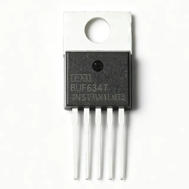
BUF634T - 250mA High-Speed Buffer, 2000V/us | Texas Instruments
BUF634T

BUF634T - 250mA High-Speed Buffer, 2000V/us | Texas Instruments

The Texas Instruments BUF634T is a 250 mA high-speed, unity-gain, open-loop buffer amplifier with a 2000 V/us slew rate, pin-selected 180 MHz bandwidth, and a wide supply range of up to plus or minus 18 V, housed in a 5-pin TO-220-5 package. A buffer amplifier (also called a unity-gain voltage follower) is a specialized amplifier stage with a gain of one that isolates a high-impedance source from a low-impedance load. In the signal-chain hierarchy, buffers sit between operational amplifiers and their loads: an op amp provides voltage gain while the buffer provides current gain, preventing load-induced distortion and thermal feedback inside the gain element. Buffers are a core building block of analog power management and output driver design. Key features of the BUF634T include 250 mA of continuous output current, an extremely fast 2000 V/us slew rate, and a unique pin-selected bandwidth mode: connecting the BW pin to V- enables the full 180 MHz bandwidth (1.5 mA typical quiescent... 30 MHz mode draws only 1.5 mA... full 180 MHz mode draws approximately 11 mA). Internal current limiting and thermal shutdown protection provide robustness against output shorts and overloads. The device is fabricated on a bipolar process optimized for speed and drive capability rather than precision offset. Architecturally, the BUF634 is a completely open-loop, unity-gain buffer, so it adds no phase shift from feedback compensation and can be placed inside an op amp feedback loop to boost output current, eliminate thermal feedback errors in the op amp input stage, and improve capacitive load drive without oscillation risk. Typical applications include headphone amplifier output stages (a classic pairing with the OPA627 or OPA134), video distribution and line driving, op amp output current boosting for test and measurement instrumentation, and capacitive load isolation for ADC input drivers and cable drivers. Design consideration: the BUF634T is not a precision amplifier - offset voltage and drift are far looser than a precision op amp, so place it inside an overall feedback loop when DC accuracy matters. Power dissipation scales with load current and supply headroom, so the TO-220-5 tab should be heat-sunk for sustained high-current operation. This page synthesizes distributor pricing, drop-in alternative analysis, and practical design notes not found in the manufacturer datasheet.

USD $9,40 Контакты
BUF634U - 250mA, 180MHz High-Speed Buffer | Texas Instruments
BUF634U

BUF634U - 250mA, 180MHz High-Speed Buffer | Texas Instruments

The Texas Instruments BUF634U is a 250 mA high-speed unity-gain open-loop buffer amplifier featuring a 2000 V/us slew rate and a pin-selected bandwidth of up to 180 MHz, housed in an 8-pin SOIC (SO-8, 3.90 mm width) surface-mount package. A buffer amplifier is a unity-gain voltage follower that isolates a high-impedance source from a low-impedance load while delivering substantial output current. Within the power-management and signal-chain hierarchy, buffers sit between amplifiers and loads, extending the drive capability of operational amplifiers, ADCs, and filters. Buffers trade voltage gain for current gain, and the BUF634 is a classic open-loop buffer architecture in which the output stage is driven directly by the input, minimizing transient distortion. Key features include 250 mA of output current, a 2000 V/us slew rate that preserves fast edges, a wide supply range of +/-2.25 V to +/-18 V (4.5 V to 36 V total), and a low 1.5 mA quiescent current when operated in the 30 MHz low-power bandwidth mode selected via the bandwidth pin. Internal current limiting and thermal shutdown protection guard the device against overload faults. Technically, the BUF634 combines a high-speed bipolar input stage with a push-pull class-AB output stage. The pin-selected bandwidth (30 MHz or 180 MHz) lets designers trade quiescent power for speed: low-power mode suits battery and portable designs, while full-bandwidth mode supports fast pulse and video signal chains. Because it is open-loop, phase reversal is not an issue and it can be placed inside an op-amp feedback loop to boost output current, eliminate thermal feedback on the input stage, and improve capacitive load drive. Typical applications include op-amp output current boosting in instrumentation amplifiers, line drivers for video and communications, headroom-limited audio headphone amplifiers, and capacitive-load driving in data-acquisition front ends. A key design consideration: the bandwidth-select pin must be tied appropriately (to V- for 180 MHz or open with capacitor for 30 MHz); leaving it floating can produce unpredictable frequency response. Note that the BUF634U is designated not recommended for new designs (NRND); TI recommends the BUF634A as a pin-compatible upgrade. This page synthesizes distributor pricing, drop-in alternatives, application guidance, and lifecycle information not consolidated in the manufacturer datasheet.

Запрос цены Контакты
BUF634U-VB - 250mA High-Speed Buffer, 180MHz SOIC-8 | Texas Instruments
BUF634U-VB

BUF634U-VB - 250mA High-Speed Buffer, 180MHz SOIC-8 | Texas Instruments

The Texas Instruments BUF634U-VB (BUF634U) is a 250 mA high-speed, unity-gain, open-loop buffer with a 2000 V/us slew rate, pin-selected bandwidth up to 180 MHz, and a wide supply range of +/-2.25 V to +/-18 V, housed in an 8-pin SOIC package. A buffer amplifier is a unity-gain stage whose purpose is to isolate a high-impedance source from a low-impedance load while passing the signal without amplification. In the signal-chain hierarchy, the buffer sits between a precision op amp and its load, providing current gain and drive capability that the op amp alone cannot deliver. High-speed buffers like the BUF634 family are essential building blocks in analog front-end design. Key features include a continuous output current of 250 mA, a 2000 V/us slew rate for fast large-signal edges, and a bandwidth that is pin-selectable between 30 MHz, 130 MHz, and 180 MHz, allowing designers to trade bandwidth against quiescent current - only 1.5 mA at the 30 MHz setting. Internal current limiting and thermal shutdown protection guard against fault conditions. Architecturally, the BUF634 is an open-loop bipolar buffer with no internal feedback compensation, which means it adds essentially no phase shift when placed inside an op amp feedback loop. This lets it boost op amp output current, eliminate thermal-feedback-induced errors, and improve capacitive-load drive without degrading loop stability. Typical applications include buffering the output of precision op amps such as the OPA-series in test and measurement instrumentation, driving ADC input or reference networks, and serving as a current booster inside audio or video line-driver loops. Design consideration: the bandwidth pin (BW) sets quiescent current, so choose the lowest bandwidth setting that meets signal requirements to minimize power dissipation and thermal rise in the SOIC-8 package. This page synthesizes verified distributor pricing, drop-in alternative analysis, and practical design guidance not found in the manufacturer datasheet.

Запрос цены Контакты
BUF634U/2K5 - 250mA 180MHz High-Speed Buffer | TI
BUF634U/2K5

BUF634U/2K5 - 250mA 180MHz High-Speed Buffer | TI

The Texas Instruments BUF634U/2K5 is a 250mA high-speed unity-gain open-loop buffer amplifier with 180MHz bandwidth, 2000 V/µs slew rate, and a wide ±18V (36V single-supply) operating range, housed in an 8-pin SOIC (D) package supplied in tape and reel. A high-speed buffer is a unity-gain amplifier optimized for output current drive and bandwidth rather than voltage gain. In the power-management and signal-chain hierarchy, it sits between an op amp and a load, extending the load-driving capability of precision amplifiers. Buffers like the BUF634 belong to the buffer amplifier family of analog ICs and are commonly placed inside an op amp feedback loop to raise output current, isolate capacitive loads, and eliminate thermal-feedback-induced distortion. Key features of the BUF634U/2K5 include 250mA output current with internal current limiting, pin-selectable bandwidth of 180MHz (full bandwidth) or 30MHz with only 1.5mA quiescent current, and thermal shutdown protection. This bandwidth-selection pin lets designers trade speed for power, making the device equally at home in fast pulse applications and battery-conscious designs. The 2000 V/µs slew rate supports large-signal high-frequency signals without slew limiting. The BUF634 uses an open-loop, high-current class-AB output topology with a quiescent bias that scales with the selected bandwidth setting. Because it operates open-loop, its gain is fixed near unity with high input impedance (5µA input bias current) and a 30mV input offset voltage, so it is normally embedded within an op amp feedback loop where loop gain corrects its offsets and gain error. Typical applications include op amp output boost stages in line drivers and ATE, laser-diode and piezo drivers, video distribution, cable and test instrumentation drivers, and capacitive-load isolation for precision amplifiers such as the OPA series. A key design consideration is thermal management: driving 250mA continuously at high supply voltage can exceed package dissipation, so copper area on the SOIC-8 footprint and the thermal shutdown threshold must be accounted for in the design. This page synthesizes distributor pricing, drop-in alternatives, pinout data, and practical design notes beyond what the manufacturer datasheet alone provides. Pricing references are as of 2026-09-13.

Запрос цены Контакты
C30627FHP - 16-bit M16C/60 MCU, 384KB Flash | Renesas
C30627FHP

C30627FHP - 16-bit M16C/60 MCU, 384KB Flash | Renesas

The Renesas C30627FHP#D5C is a legacy 16-bit single-chip CMOS microcontroller from the M16C/60 platform (M16C/60/62P group), offered in a 128-pin LFQFP package (14x20 mm). It integrates 384 KB of on-chip flash memory, runs at up to 24 MHz core clock from a 3 V to 5 V supply, and is positioned by Renesas as a long-lifecycle MCU for industrial automation, EMS production equipment, and process-control systems. A 16-bit microcontroller (MCU) is an embedded processor with a 16-bit data path, registers, and ALU, sitting between 8-bit entry-level MCUs (e.g., 8051) and 32-bit application processors (e.g., ARM Cortex-M). The M16C family is a classic CISC-style 16-bit architecture from Mitsubishi/Renesas known for deterministic interrupt latency, low EMI, and code-density efficiency, with an instruction set that often outperforms 8-bit parts in bytes-per-function. The M30627 derivative serves as a '60-series' general-purpose MCU within the broader M16C/60/62P hierarchy, mapping into Renesas's industrial MCU lineup. Key features of the C30627FHP include 384 KB flash, 31 KB RAM, a 10-bit A/D converter with up to 16 analog channels, multiple timers, UART/SIO/I2C peripherals, and watchdog / voltage-detection safety functions. The wide 3 V to 5 V operating range and industrial temperature grade make it suitable for factory-floor hardware that must survive electrical noise and extended thermal stress. Architecturally, the M16C core combines a compact 16-bit ALU with a rich peripheral set and an instruction set engineered for high code density, helping designers fit more functionality into 384 KB than equivalent 8-bit programs would allow. Internal bus arbitration, DMA, and address-space extensions are tuned for real-time control loops rather than large OS workloads, distinguishing it from higher-end 32-bit MCUs. Typical applications include industrial PLCs and motor-control boards, inverter drives, process-control instrumentation, building automation controllers, and EMS production-line equipment where the C30627FHP's combination of deterministic interrupts, multi-channel ADC, and long-term availability are valued. As an EOL-prone legacy part, it is most often specified in equipment whose design must remain frozen for years. When sourcing, verify the exact suffix (e.g., #D5C, #U5C) and package code against the datasheet, because the M30627 family has multiple pin-compatible speed grades, voltage variants, and reel codes that share the same 128-LFQFP footprint but differ in mask ROM, flash density, or temp grade. Plan for lifecycle risk: this part is reaching end-of-life, so design-in of a modern M16C or RL78 successor is recommended for new programs. This page synthesizes distributor pricing, drop-in same-family alternatives, and practical design notes not found in the bare Renesas datasheet.

Запрос цены Контакты
C505CA4EMCA - 8-Bit MCU, 12MHz, OTP, 32 I/O | Infineon
C505CA4EMCA

C505CA4EMCA - 8-Bit MCU, 12MHz, OTP, 32 I/O | Infineon

The Infineon C505CA4EMCA (full designation SAK-C505CA-4EMCA) is an 8-bit single-chip CMOS microcontroller based on the industry-standard 8051 architecture, delivering up to 12 MHz clock speed and housed in a 44-pin MQFP package. It integrates 32 programmable I/O lines, an on-chip OTP (One-Time Programmable) ROM, and a wide 4.25V to 5.5V supply voltage range, making it suitable for industrial-grade embedded control applications. An 8-bit microcontroller (MCU) is a programmable processor that executes instructions from internal ROM/RAM, communicates with peripherals through digital I/O pins, and integrates timers, interrupts, and serial interfaces on a single silicon die. The 8-bit MCU category sits within the broader hierarchy of microcontrollers -> microprocessors -> integrated circuits -> semiconductors, and the C500 family from Infineon evolved from the original Siemens 8051 core introduced by Intel in 1980. Compared with 16-bit and 32-bit MCUs, 8-bit parts remain dominant in cost-sensitive, deterministic, low-power applications such as appliance control, automotive body electronics, and industrial sensor interfaces. Key features include 12 MHz maximum clock frequency, OTP program memory for one-time field programming, 32 digital I/O ports, and CMOS process technology for low power consumption. The supply voltage range of 4.25V to 5.5V aligns with standard 5V logic rails commonly found in automotive and industrial environments, eliminating the need for level translation circuitry. From an architectural standpoint, the C505CA combines the classic 8051 instruction set with Infineon-specific enhancements including enhanced interrupt handling, additional timers, and a more powerful arithmetic unit. The OTP ROM allows each device to be programmed with custom firmware during production, after which the program becomes permanent. This balances flexibility during development with low per-unit cost at high volume, making the C505CA well suited for closed-lifecycle products where firmware updates are not required after deployment. Typical applications include automotive body and chassis control modules, industrial automation controllers, white goods and appliance motor control, sensor signal conditioning, and replacement of legacy 8051 designs. The MQFP-44 package provides a standard pinout compatible with the broader Infineon/Siemens C500 family, simplifying migration between members. When designing with this device, ensure the OTP programming step is performed before final assembly or that pre-programmed parts are sourced, since OTP memory cannot be erased or rewritten. Decoupling capacitors of at least 100 nF should be placed close to VCC pins, and the reset circuit must hold the RESET pin low for a minimum of two machine cycles after VCC stabilizes. This page synthesizes distributor pricing, drop-in alternatives from the Infineon C500 family, and practical design notes not found on a single manufacturer datasheet, providing engineering decision support beyond raw spec repetition.

Запрос цены Контакты
C8051F000 - 20 MIPS Mixed-Signal 32KB Flash MCU | Silicon Labs
C8051F000

C8051F000 - 20 MIPS Mixed-Signal 32KB Flash MCU | Silicon Labs

The Silicon Labs C8051F000 is an 8-bit mixed-signal microcontroller operating at up to 20 MIPS, with 32 KB of ISP flash memory, 256 x 8 RAM, a 12-bit SAR ADC, and a 64-pin TQFP (10 x 10 mm) package. Its integrated analog peripherals make it suitable for industrial measurement, control, sensor acquisition, data logging, and embedded systems requiring more than a basic digital MCU. A mixed-signal MCU combines a digital microcontroller core with analog-to-digital, digital-to-analog, comparator, and sensor functions on one integrated circuit. The C8051F000 belongs to the 8051-compatible microcontroller hierarchy, where the CPU executes firmware while the on-chip analog subsystem measures or generates physical signals. This integration reduces external component count and simplifies PCB layouts for acquisition and control systems. Key features include a maximum 20 MHz clock performance stated as 20 MIPS, a 9-channel ADC input multiplexer, a programmable-gain amplifier, 100 ksps maximum ADC throughput, and true 12-bit accuracy with ±1 LSB INL. The device also includes a 12-bit, two-channel DAC, two comparators, an on-chip temperature sensor, programmable windowed interrupt generation, and an on-chip JTAG debug interface. The C8051F000 is based on the CIP-51 core and is designed for mixed-signal embedded control rather than high-volume connectivity. Its ISP flash supports in-system programming, while the integrated debug circuitry allows full-speed, non-intrusive debugging with the production device installed in the application. These features help shorten firmware development and bring-up cycles compared with a system requiring a separate debug interface. Typical applications include industrial process monitoring, environmental sensor interfaces, laboratory instrumentation, motor and actuator control, data acquisition, and embedded control systems. The ADC can sample analog inputs at up to 100 ksps, while the DAC provides programmable analog outputs for control or signal-generation tasks. The integrated temperature sensor is useful for local monitoring when its accuracy and calibration requirements match the application. The principal design consideration is analog signal conditioning. The ADC input multiplexer, programmable gain amplifier, reference selection, sampling timing, and analog-ground layout determine usable resolution and repeatability. Engineers should follow the manufacturer datasheet for pin multiplexing, bypass capacitors, clock requirements, and peripheral configuration rather than assuming that nominal 12-bit resolution guarantees accurate results in every PCB environment. This product data combines the verified manufacturer datasheet information, distributor package and core details, and practical mixed-signal design considerations. It is intended to help engineers identify the correct MCU package, memory configuration, analog resources, and application fit before purchasing or replacing the device.

Запрос цены Контакты
C8051F000R - 20 MIPS Mixed-Signal 32KB Flash MCU | Silicon Labs (Tape & Reel)
C8051F000R

C8051F000R - 20 MIPS Mixed-Signal 32KB Flash MCU | Silicon Labs (Tape & Reel)

The Silicon Labs C8051F000R is an 8-bit mixed-signal microcontroller operating at up to 20 MIPS, with 32 KB of ISP flash memory, 256 x 8 RAM, a 12-bit SAR ADC, and a 64-pin TQFP (10 x 10 mm) package. Its integrated analog peripherals make it suitable for industrial measurement, control, sensor acquisition, data logging, and embedded systems requiring more than a basic digital MCU. A mixed-signal MCU combines a digital microcontroller core with analog-to-digital, digital-to-analog, comparator, and sensor functions on one integrated circuit. The C8051F000R belongs to the 8051-compatible microcontroller hierarchy, where the CPU executes firmware while the on-chip analog subsystem measures or generates physical signals. This integration reduces external component count and simplifies PCB layouts for acquisition and control systems. Key features include a maximum 20 MHz clock performance stated as 20 MIPS, a 9-channel ADC input multiplexer, a programmable-gain amplifier, 100 ksps maximum ADC throughput, and true 12-bit accuracy with ±1 LSB INL. The device also includes a 12-bit, two-channel DAC, two comparators, an on-chip temperature sensor, programmable windowed interrupt generation, and an on-chip JTAG debug interface. The C8051F000R is based on the CIP-51 core and is designed for mixed-signal embedded control rather than high-volume connectivity. Its ISP flash supports in-system programming, while the integrated debug circuitry allows full-speed, non-intrusive debugging with the production device installed in the application. These features help shorten firmware development and bring-up cycles compared with a system requiring a separate debug interface. Typical applications include industrial process monitoring, environmental sensor interfaces, laboratory instrumentation, motor and actuator control, data acquisition, and embedded control systems. The ADC can sample analog inputs at up to 100 ksps, while the DAC provides programmable analog outputs for control or signal-generation tasks. The integrated temperature sensor is useful for local monitoring when its accuracy and calibration requirements match the application. The principal design consideration is analog signal conditioning. The ADC input multiplexer, programmable gain amplifier, reference selection, sampling timing, and analog-ground layout determine usable resolution and repeatability. Engineers should follow the manufacturer datasheet for pin multiplexing, bypass capacitors, clock requirements, and peripheral configuration rather than assuming that nominal 12-bit resolution guarantees accurate results in every PCB environment. This product data combines the verified manufacturer datasheet information, distributor package and core details, and practical mixed-signal design considerations. It is intended to help engineers identify the correct MCU package, memory configuration, analog resources, and application fit before purchasing or replacing the device.

Запрос цены Контакты
C8051F001 - 20MHz 32KB Flash Mixed-Signal MCU | Silicon Labs
C8051F001

C8051F001 - 20MHz 32KB Flash Mixed-Signal MCU | Silicon Labs

The Silicon Labs C8051F001 is a mixed-signal 8-bit microcontroller with a 20 MHz 8051 core, 32 KB of flash memory, and a 48-pin TQFP package measuring 7 mm by 7 mm. Its principal verified specifications include 12-bit ADC and DAC resolution, an eight-channel ADC operating at up to 100 ksps, a two-channel DAC, two comparators, and an on-chip temperature sensor. The device combines embedded control, data acquisition, and analog output in one package. A mixed-signal microcontroller is an integrated circuit that places a digital processor and analog conversion or comparison functions on the same device. The C8051F001 belongs to the 8051 CISC microcontroller family and combines a CIP-51-class 8-bit processing core with ADC, DAC, comparator, and sensor functions. This integration can reduce board count in measurement, control, and industrial systems that require both digital computation and analog signal handling. The C8051F001 provides 32 KB of flash program memory and is identified in distributor data as the C8051F00x mixed-signal microcontroller family member. Its ADC offers 12-bit resolution across eight channels at up to 100 ksps, while the DAC provides 12-bit resolution on two channels. Two comparators and an integrated temperature sensor broaden the peripheral set beyond basic digital GPIO and timer functions. The manufacturer data sheet identifies the C8051F001 as part of the C8051F00x/01x family and specifically confirms its availability in a 48-pin TQFP package. The verified distributor listing specifies a 7 mm by 7 mm package and a 20 MHz operating frequency. This combination makes the device appropriate for embedded acquisition, industrial instrumentation, control panels, sensor conditioning, and compact mixed-signal control products. When designing around this MCU, verify the complete 48-pin mapping and all analog, reference, ground, supply, programming, and oscillator connections against the manufacturer data sheet before layout. Analog acquisition performance depends on proper reference selection, grounding, decoupling, and signal conditioning as well as the nominal 12-bit converter resolution. Firmware and peripheral configuration should likewise be checked against the exact C8051F001 device documentation. This page consolidates verified manufacturer and distributor information about the C8051F001, including package, memory, conversion, and interface characteristics. It also distinguishes confirmed facts from specifications that still require confirmation, helping engineers evaluate procurement and design risks before committing an existing 8051-based product to production.

Запрос цены Контакты
C8051F001R - 20MHz 32KB Flash Mixed-Signal MCU | Silicon Labs (Tape & Reel)
C8051F001R

C8051F001R - 20MHz 32KB Flash Mixed-Signal MCU | Silicon Labs (Tape & Reel)

The Silicon Labs C8051F001R is a mixed-signal 8-bit microcontroller with a 20 MHz 8051 core, 32 KB of flash memory, and a 48-pin TQFP package measuring 7 mm by 7 mm. Its principal verified specifications include 12-bit ADC and DAC resolution, an eight-channel ADC operating at up to 100 ksps, a two-channel DAC, two comparators, and an on-chip temperature sensor. The device combines embedded control, data acquisition, and analog output in one package. A mixed-signal microcontroller is an integrated circuit that places a digital processor and analog conversion or comparison functions on the same device. The C8051F001R belongs to the 8051 CISC microcontroller family and combines a CIP-51-class 8-bit processing core with ADC, DAC, comparator, and sensor functions. This integration can reduce board count in measurement, control, and industrial systems that require both digital computation and analog signal handling. The C8051F001R provides 32 KB of flash program memory and is identified in distributor data as the C8051F00x mixed-signal microcontroller family member. Its ADC offers 12-bit resolution across eight channels at up to 100 ksps, while the DAC provides 12-bit resolution on two channels. Two comparators and an integrated temperature sensor broaden the peripheral set beyond basic digital GPIO and timer functions. The manufacturer data sheet identifies the C8051F001R as part of the C8051F00x/01x family and specifically confirms its availability in a 48-pin TQFP package. The verified distributor listing specifies a 7 mm by 7 mm package and a 20 MHz operating frequency. This combination makes the device appropriate for embedded acquisition, industrial instrumentation, control panels, sensor conditioning, and compact mixed-signal control products. When designing around this MCU, verify the complete 48-pin mapping and all analog, reference, ground, supply, programming, and oscillator connections against the manufacturer data sheet before layout. Analog acquisition performance depends on proper reference selection, grounding, decoupling, and signal conditioning as well as the nominal 12-bit converter resolution. Firmware and peripheral configuration should likewise be checked against the exact C8051F001R device documentation. This page consolidates verified manufacturer and distributor information about the C8051F001R, including package, memory, conversion, and interface characteristics. It also distinguishes confirmed facts from specifications that still require confirmation, helping engineers evaluate procurement and design risks before committing an existing 8051-based product to production.

Запрос цены Контакты
C8051F002 - 20MHz 32KB Flash Mixed-Signal MCU | Silicon Labs
C8051F002

C8051F002 - 20MHz 32KB Flash Mixed-Signal MCU | Silicon Labs

The Silicon Labs C8051F002 is an 8-bit mixed-signal microcontroller MCU featuring a 20 MHz 8051 core, 32 KB flash program memory, and 32-LQFP (7x7 mm) packaging. The verified product listing identifies 32K x 8 flash memory, while the manufacturer datasheet identifies the C8051F002/07/12/17 devices as 32-pin mixed-signal MCUs. Its mixed-signal feature set supports embedded control designs requiring both digital processing and analog measurement. What is a mixed-signal MCU? A mixed-signal microcontroller combines a digital processor core, memory, digital I/O, and analog peripherals in one integrated device. Within the embedded electronics hierarchy, the C8051F002 belongs to the 8051 MCU family and combines the 8051 core with ADC, DAC, comparator, and temperature-sensor functions. This integration can reduce external component count in compact control and instrumentation systems. Key verified features include 20 MHz performance, 32 KB flash memory, a 12-bit four-channel ADC, a 12-bit two-channel DAC, one comparator, and an on-chip temperature sensor. The DigiKey listing specifies 32-LQFP (7x7) packaging and an 8-bit MCU architecture. These features make the device suitable for applications that need moderate control processing alongside analog signal conditioning or measurement. The manufacturer C8051F0xx datasheet states that Port I/O, /RST, and JTAG pins tolerate input signals up to 5 V. The same document groups the C8051F002 with the 32-pin LQFP variants. The supplied search results also state 2.7 V to 3.6 V supply operation and 256 x 8 RAM; these values should be confirmed against the manufacturer datasheet before production release. Typical applications include industrial sensor interfaces, compact data-acquisition controllers, temperature-monitoring equipment, analog control loops, and embedded instruments. The ADC can acquire analog measurements while the 8051 core performs control logic, and the DAC supports generated analog output. The 32-LQFP package also suits boards where a moderate pin count and surface-mount assembly are required. Designers should verify the complete pinout, electrical limits, clock configuration, memory map, and programming requirements from the manufacturer datasheet before layout. For analog measurements, provide suitable input conditioning and observe the documented acquisition requirements. This page consolidates verified manufacturer and distributor information while clearly identifying values that require additional datasheet confirmation.

Запрос цены Контакты
C8051F002R - 20MHz 32KB Flash Mixed-Signal MCU | Silicon Labs (Tape & Reel)
C8051F002R

C8051F002R - 20MHz 32KB Flash Mixed-Signal MCU | Silicon Labs (Tape & Reel)

The Silicon Labs C8051F002R is an 8-bit mixed-signal microcontroller MCU featuring a 20 MHz 8051 core, 32 KB flash program memory, and 32-LQFP (7x7 mm) packaging. The verified product listing identifies 32K x 8 flash memory, while the manufacturer datasheet identifies the C8051F002R/07/12/17 devices as 32-pin mixed-signal MCUs. Its mixed-signal feature set supports embedded control designs requiring both digital processing and analog measurement. What is a mixed-signal MCU? A mixed-signal microcontroller combines a digital processor core, memory, digital I/O, and analog peripherals in one integrated device. Within the embedded electronics hierarchy, the C8051F002R belongs to the 8051 MCU family and combines the 8051 core with ADC, DAC, comparator, and temperature-sensor functions. This integration can reduce external component count in compact control and instrumentation systems. Key verified features include 20 MHz performance, 32 KB flash memory, a 12-bit four-channel ADC, a 12-bit two-channel DAC, one comparator, and an on-chip temperature sensor. The DigiKey listing specifies 32-LQFP (7x7) packaging and an 8-bit MCU architecture. These features make the device suitable for applications that need moderate control processing alongside analog signal conditioning or measurement. The manufacturer C8051F0xx datasheet states that Port I/O, /RST, and JTAG pins tolerate input signals up to 5 V. The same document groups the C8051F002R with the 32-pin LQFP variants. The supplied search results also state 2.7 V to 3.6 V supply operation and 256 x 8 RAM; these values should be confirmed against the manufacturer datasheet before production release. Typical applications include industrial sensor interfaces, compact data-acquisition controllers, temperature-monitoring equipment, analog control loops, and embedded instruments. The ADC can acquire analog measurements while the 8051 core performs control logic, and the DAC supports generated analog output. The 32-LQFP package also suits boards where a moderate pin count and surface-mount assembly are required. Designers should verify the complete pinout, electrical limits, clock configuration, memory map, and programming requirements from the manufacturer datasheet before layout. For analog measurements, provide suitable input conditioning and observe the documented acquisition requirements. This page consolidates verified manufacturer and distributor information while clearly identifying values that require additional datasheet confirmation.

Запрос цены Контакты
C8051F005 - 25MHz 32KB Flash Mixed-Signal MCU | Silicon Labs
C8051F005

C8051F005 - 25MHz 32KB Flash Mixed-Signal MCU | Silicon Labs

The Silicon Labs C8051F005 is a mixed-signal 8-bit microcontroller with a 25 MHz, 25 MIPS 8051 core, 32 KB of flash program memory and a 64-TQFP package. It also integrates a 12-bit ADC and two 12-bit DACs, making it suitable for embedded control and analog signal-chain designs. What is a mixed-signal microcontroller? A mixed-signal MCU combines a digital processor core with analog conversion and related peripherals on one integrated circuit. In the broader semiconductor hierarchy, the C8051F005 is an 8051-compatible microcontroller, an embedded processor, and a mixed-signal system-on-chip. Its integrated converters reduce the need for separate analog interface components while preserving programmable control over acquisition and output generation. Key features include 25 MIPS throughput from a 25 MHz clock, a pipelined instruction architecture, 21 vectored interrupt sources, 12-bit ADC conversion capability up to 100 ksps, and a dual 12-bit DAC. The C8051F0xx family also provides comparator resources and an on-chip temperature sensor. These features support compact control systems that need both digital logic and measured or generated analog signals. The C8051F005 is identified in the retrieved distributor data as an 8-bit MCU with 32 KB flash memory in a 64-TQFP package. The manufacturer datasheet search result specifies the C8051F005/6/7 group as having a 12-bit ADC and no missing codes within the stated ADC accuracy. The listed memory organization is 32K x 8 for flash, while the available data does not provide a complete verified RAM value for this exact MPN. Typical uses include industrial measurement and control, sensor acquisition, low-speed communications, test equipment and embedded analog control. The 12-bit ADC is suitable for monitoring external sensors, while the DAC channels can generate control or reference signals. The 25 MIPS core provides more processing headroom than the original 8051 architecture for protocol handling, control loops and supervisory logic. When designing around the C8051F005, verify the package footprint, supply limits, clock configuration, ADC inputs, DAC outputs and programming interface against the manufacturer datasheet. Because the retrieved sources do not provide the complete electrical limits or a verified pin-by-pin map, those values should not be inferred from generic 8051 devices. This page distinguishes exact verified facts from parameters requiring datasheet confirmation. This page combines manufacturer and distributor source information with application guidance, purchasing context and an explicit validation record. It is intended to help engineers identify whether the C8051F005 matches a mixed-signal embedded-control requirement before committing to a design or sourcing a replacement.

Запрос цены Контакты
C8051F005R - 25MHz 32KB Flash Mixed-Signal MCU | Silicon Labs (Tape & Reel)
C8051F005R

C8051F005R - 25MHz 32KB Flash Mixed-Signal MCU | Silicon Labs (Tape & Reel)

The Silicon Labs C8051F005R is a mixed-signal 8-bit microcontroller with a 25 MHz, 25 MIPS 8051 core, 32 KB of flash program memory and a 64-TQFP package. It also integrates a 12-bit ADC and two 12-bit DACs, making it suitable for embedded control and analog signal-chain designs. What is a mixed-signal microcontroller? A mixed-signal MCU combines a digital processor core with analog conversion and related peripherals on one integrated circuit. In the broader semiconductor hierarchy, the C8051F005R is an 8051-compatible microcontroller, an embedded processor, and a mixed-signal system-on-chip. Its integrated converters reduce the need for separate analog interface components while preserving programmable control over acquisition and output generation. Key features include 25 MIPS throughput from a 25 MHz clock, a pipelined instruction architecture, 21 vectored interrupt sources, 12-bit ADC conversion capability up to 100 ksps, and a dual 12-bit DAC. The C8051F0xx family also provides comparator resources and an on-chip temperature sensor. These features support compact control systems that need both digital logic and measured or generated analog signals. The C8051F005R is identified in the retrieved distributor data as an 8-bit MCU with 32 KB flash memory in a 64-TQFP package. The manufacturer datasheet search result specifies the C8051F005R/6/7 group as having a 12-bit ADC and no missing codes within the stated ADC accuracy. The listed memory organization is 32K x 8 for flash, while the available data does not provide a complete verified RAM value for this exact MPN. Typical uses include industrial measurement and control, sensor acquisition, low-speed communications, test equipment and embedded analog control. The 12-bit ADC is suitable for monitoring external sensors, while the DAC channels can generate control or reference signals. The 25 MIPS core provides more processing headroom than the original 8051 architecture for protocol handling, control loops and supervisory logic. When designing around the C8051F005R, verify the package footprint, supply limits, clock configuration, ADC inputs, DAC outputs and programming interface against the manufacturer datasheet. Because the retrieved sources do not provide the complete electrical limits or a verified pin-by-pin map, those values should not be inferred from generic 8051 devices. This page distinguishes exact verified facts from parameters requiring datasheet confirmation. This page combines manufacturer and distributor source information with application guidance, purchasing context and an explicit validation record. It is intended to help engineers identify whether the C8051F005R matches a mixed-signal embedded-control requirement before committing to a design or sourcing a replacement.

Запрос цены Контакты
C8051F006 - 25MHz 32KB Flash Mixed-Signal MCU | Silicon Labs
C8051F006

C8051F006 - 25MHz 32KB Flash Mixed-Signal MCU | Silicon Labs

The Silicon Labs C8051F006 is a highly integrated mixed-signal 8-bit microcontroller with a 25 MHz CIP-51 core, 32 KB of flash program memory, a 12-bit 8-channel ADC, a 12-bit 2-channel DAC, two comparators, and an on-chip temperature sensor. The device is supplied in a 48-pin TQFP package and operates from a 2.7 V to 3.6 V supply. Its combination of 8051-compatible processing, analog measurement, and programmable digital peripherals makes it suitable for embedded control, sensor acquisition, and industrial instrumentation designs. A microcontroller is a programmable semiconductor that integrates a CPU core, memory, and peripheral functions on one die. The C8051F006 belongs to the 8-bit MCU category, with the CIP-51 core providing higher sustained performance than a conventional 8051 while retaining the familiar 8051 instruction set. Mixed-signal variants such as this device extend the MCU hierarchy by integrating converters, comparators, and sensor interfaces alongside digital control logic. Key features include 25 MIPS execution capability, 32 KB of flash memory, 2.25 KB of RAM, 12-bit ADC resolution, and 100 ksps ADC throughput. The dual 12-bit DAC supports waveform generation or analog output, while two comparators can monitor external signals and trigger interrupt-driven control events. A programmable internal oscillator and oscillator-enable features support flexible clocking, while UART, SPI, SMBus, and timers provide standard embedded communication and event-management functions. The C8051F000 family architecture is designed for mixed-signal control rather than simple logic replacement. Its ADC can operate in multiple sampling modes, and the analog peripherals are supported by an analog subsystem that helps applications acquire and compare low-level sensor signals without requiring separate converters. The 25 MHz core also provides enough computational headroom for protocol handling, control-loop execution, and system supervision in a single device. Typical uses include industrial process measurement, environmental monitoring, sensor interfaces, data acquisition, embedded instrumentation, and compact control systems. The 100 ksps 12-bit ADC is particularly useful for ratiometric or moderate-speed analog measurement, while the DAC enables excitation, reference, or control outputs. The integrated temperature sensor also supports local thermal monitoring in equipment where a separate sensor would add cost and board area. Designers should verify the complete pinout, electrical limits, and peripheral configuration in the manufacturer datasheet before committing the PCB layout. Decoupling should follow the device requirements, unused inputs should be handled according to the datasheet, and analog signal routing should be separated from fast digital switching paths. Firmware must also account for the selected oscillator configuration and the analog peripheral settling behavior. This page combines verified distributor specifications, package and ordering information, application guidance, and a structured replacement analysis. It also distinguishes confirmed drop-in alternatives from redesign-level candidates, helping engineers make sourcing and board-layout decisions without treating merely similar microcontrollers as interchangeable.

Запрос цены Контакты
C8051F006R - 25MHz 32KB Flash Mixed-Signal MCU | Silicon Labs (Tape & Reel)
C8051F006R

C8051F006R - 25MHz 32KB Flash Mixed-Signal MCU | Silicon Labs (Tape & Reel)

The Silicon Labs C8051F006R is a highly integrated mixed-signal 8-bit microcontroller with a 25 MHz CIP-51 core, 32 KB of flash program memory, a 12-bit 8-channel ADC, a 12-bit 2-channel DAC, two comparators, and an on-chip temperature sensor. The device is supplied in a 48-pin TQFP package and operates from a 2.7 V to 3.6 V supply. Its combination of 8051-compatible processing, analog measurement, and programmable digital peripherals makes it suitable for embedded control, sensor acquisition, and industrial instrumentation designs. A microcontroller is a programmable semiconductor that integrates a CPU core, memory, and peripheral functions on one die. The C8051F006R belongs to the 8-bit MCU category, with the CIP-51 core providing higher sustained performance than a conventional 8051 while retaining the familiar 8051 instruction set. Mixed-signal variants such as this device extend the MCU hierarchy by integrating converters, comparators, and sensor interfaces alongside digital control logic. Key features include 25 MIPS execution capability, 32 KB of flash memory, 2.25 KB of RAM, 12-bit ADC resolution, and 100 ksps ADC throughput. The dual 12-bit DAC supports waveform generation or analog output, while two comparators can monitor external signals and trigger interrupt-driven control events. A programmable internal oscillator and oscillator-enable features support flexible clocking, while UART, SPI, SMBus, and timers provide standard embedded communication and event-management functions. The C8051F000 family architecture is designed for mixed-signal control rather than simple logic replacement. Its ADC can operate in multiple sampling modes, and the analog peripherals are supported by an analog subsystem that helps applications acquire and compare low-level sensor signals without requiring separate converters. The 25 MHz core also provides enough computational headroom for protocol handling, control-loop execution, and system supervision in a single device. Typical uses include industrial process measurement, environmental monitoring, sensor interfaces, data acquisition, embedded instrumentation, and compact control systems. The 100 ksps 12-bit ADC is particularly useful for ratiometric or moderate-speed analog measurement, while the DAC enables excitation, reference, or control outputs. The integrated temperature sensor also supports local thermal monitoring in equipment where a separate sensor would add cost and board area. Designers should verify the complete pinout, electrical limits, and peripheral configuration in the manufacturer datasheet before committing the PCB layout. Decoupling should follow the device requirements, unused inputs should be handled according to the datasheet, and analog signal routing should be separated from fast digital switching paths. Firmware must also account for the selected oscillator configuration and the analog peripheral settling behavior. This page combines verified distributor specifications, package and ordering information, application guidance, and a structured replacement analysis. It also distinguishes confirmed drop-in alternatives from redesign-level candidates, helping engineers make sourcing and board-layout decisions without treating merely similar microcontrollers as interchangeable.

Запрос цены Контакты
C8051F007 - 25MHz Mixed-Signal 32KB Flash MCU | Silicon Labs
C8051F007

C8051F007 - 25MHz Mixed-Signal 32KB Flash MCU | Silicon Labs

The Silicon Labs C8051F007 is a mixed-signal 8-bit microcontroller with a 25 MIPS 8051 core, 32 KB of ISP flash memory, 2.25 KB of RAM, and eight I/O pins in a 32-LQFP package. Its integrated mixed-signal resources include a 12-bit, four-channel, 100 ksps ADC, a 12-bit, two-channel DAC, one comparator, and an on-chip temperature sensor. The device operates from a 2.7 V to 3.6 V supply and is intended for compact embedded-control systems that require both digital processing and analog measurement or output capability. A mixed-signal microcontroller is an embedded semiconductor that combines a digital processor core with analog conversion and comparison functions. The C8051F007 belongs to the 8051 microcontroller hierarchy: its C8051F00x family architecture combines a legacy-compatible 8-bit processing core with flash memory, on-chip peripherals, and mixed-signal conversion blocks. This integration reduces the component count and board area required for designs that measure analog inputs and generate controlled analog outputs. Key features include 25 MIPS processing performance, 32 KB of ISP flash, 2.25 KB of RAM, a four-channel 12-bit ADC capable of 100 ksps conversion, and a dual-channel 12-bit DAC. The 2.7 V to 3.6 V operating range suits low-voltage embedded systems, while eight I/O pins provide digital control and status signaling. The integrated comparator and temperature sensor extend the device beyond basic data acquisition, enabling local threshold detection and temperature-oriented designs without additional external ICs. The enhanced 8051 core provides a practical balance between processing capability and design familiarity. ISP flash supports programming in circuit, while integrated analog peripherals reduce conversion-system complexity. At 25 MIPS, the C8051F007 is suitable for supervisory control loops, signal conditioning, sensor interfaces, and compact industrial or instrumentation systems. Because this is an 8-bit MCU with limited RAM, software should use the available memory efficiently and avoid treating it as a high-bandwidth signal-processing platform. Typical uses include industrial process-control modules, temperature-monitoring instruments, motor and actuator controllers, laboratory measurement equipment, sensor conditioning, and compact embedded data-acquisition systems. The ADC supports four analog inputs, while the DAC can generate two controlled analog outputs. These resources make the MCU appropriate for systems where a single device must supervise digital logic while also acquiring measurements and driving analog control signals. Designers should verify the complete pinout and analog operating details in the manufacturer C8051F0xx datasheet before layout because the verified source set does not provide a reliable numbered pin list. Analog inputs, DAC outputs, supply pins, oscillator connections, and programming signals also require normal signal-integrity, grounding, and decoupling practices. The 2.7 V minimum supply and 3.6 V maximum supply must be respected throughout startup, measurement, and output conditions. This product page combines the verified 25 MIPS, 32 KB flash, 12-bit ADC, DAC, comparator, temperature-sensor, package, supply-voltage, RAM, and I/O information with same-family replacement guidance and practical selection notes. It also distinguishes verified facts from parameters that still require confirmation from the full manufacturer datasheet.

Запрос цены Контакты
C8051F007R - 25MHz 8051 MCU with 32KB Flash | Silicon Labs
C8051F007R

C8051F007R - 25MHz 8051 MCU with 32KB Flash | Silicon Labs

The Silicon Labs C8051F007R is an 8-bit C8051F00x-series microcontroller operating at up to 25 MHz, with 32 KB of programmable Flash memory, 2.25 KB of RAM, and eight general-purpose I/O pins in a 32-pin LQFP package. It operates from a 2.7 V to 3.6 V supply and combines the enhanced 8051 core with integrated flash memory for compact embedded control designs. An 8-bit microcontroller is a programmable semiconductor containing a central processing unit, memory, and peripheral interfaces on one integrated circuit. The C8051F00x family uses a CIP-51-compatible enhanced 8051 architecture, making it part of the broader embedded-controller and microcontroller hierarchy. Its combination of Flash memory, digital I/O, serial communication capability, and analog conversion functions allows a single device to supervise sensors, actuators, communications, and industrial control logic. The principal specifications include a 25 MHz maximum clock, 32 KB of 8-bit Flash program memory, 2.25 KB of 8-bit RAM, eight I/O lines, and a 2.7 V to 3.6 V operating supply range. The program-memory capacity supports substantially larger firmware than the smaller members of the C8051F00x family, while the LQFP-32 package provides enough pins for external interface and signal-conditioning requirements. The enhanced 8051 architecture is designed for efficient embedded execution and compatibility with established 8051 development workflows. Internal peripherals reduce the need for separate logic devices, while the Flash-based program memory permits field reprogramming and simplifies firmware maintenance. Because the device operates from a 3.3 V supply range, system-level design should account for voltage levels, clock requirements, decoupling, and the electrical limits of connected sensors and actuators. Typical applications include industrial control modules, data-acquisition equipment, environmental monitoring, serial-interface controllers, compact instrumentation, and embedded communication equipment. The 32 KB Flash capacity is useful for protocol handling, state-machine control, diagnostics, and configurable product functions, while the eight I/O pins support digital control and communication signaling. For PCB implementation, place the required supply bypass capacitors close to the supply pins and route the clock network away from high-current switching nodes. Confirm the exact pin assignments, analog input limits, oscillator options, and programming connections against the manufacturer datasheet before releasing the PCB or firmware. This product page combines the device's core specifications, verified source links, same-family drop-in considerations, comparison parameters, and practical integration guidance. It supports faster component identification while keeping PCB compatibility and firmware migration requirements at the center of the selection process.

Запрос цены Контакты
C8051F010 - 20MHz 32KB Mixed-Signal MCU | Silicon Labs
C8051F010

C8051F010 - 20MHz 32KB Mixed-Signal MCU | Silicon Labs

Silicon Labs C8051F010 is an 8-bit mixed-signal microcontroller with a 20 MHz clock, 32KB flash memory and a 64-pin TQFP package. The verified distributor data identifies 256 bytes of RAM, 32 I/O pins and a maximum 100 ksps ADC throughput. Its integrated analog resources include a 10-bit, 8-channel ADC, a 12-bit, 2-channel DAC, two comparators and an on-chip temperature sensor, making it suitable for embedded measurement and control systems. A mixed-signal MCU combines a digital processor and analog peripherals in one semiconductor package. In the broader hierarchy, the C8051F010 is an 8051-compatible microcontroller, an embedded processor and a system-on-chip device for industrial control. Its integrated converters reduce the need for separate analog components while preserving a compact, 64-pin surface-mount design. The C8051F010 runs at 20 MHz and provides 32KB of flash program storage plus 256 bytes of RAM. The verified data describes a 10-bit ADC with eight channels and throughput up to 100 ksps, along with a two-channel 12-bit DAC. An internal 15 ppm voltage reference is available, and an external reference can also be used where the application requires independent accuracy. The device also includes two comparators, an on-chip temperature sensor and 32 I/O pins. The C8051F0xx datasheet states that the ADC in the C8051F010/1/2/5/6/7 is similar to the other family members but provides true 10-bit accuracy for the C8051F01x variants. The verified specifications identify the C8051F010 as the 20 MHz, 32KB-flash member of the C8051F01x family. Typical uses include industrial sensor acquisition, temperature measurement, process control, embedded instrumentation and compact analog control systems. The ADC can sample multiple analog inputs, while the DAC supports programmable analog outputs; together, these functions are useful in closed-loop equipment where board area and component count matter. Designers should verify the complete pin assignment, oscillator requirements, analog-reference configuration and programming method against the manufacturer datasheet before layout. Because the available data does not include electrical limits, timing margins or a complete verified pin list, those values must not be inferred. The C8051F010 should be selected when its 8051 architecture, mixed-signal peripherals and 64-pin footprint match the existing firmware and PCB design. This page consolidates verified distributor listings, manufacturer-family specifications, datasheet references and cross-reference results for faster component identification. It distinguishes confirmed C8051F010 data from missing details and avoids treating generic substitute-search results as guaranteed drop-in replacements.

Запрос цены Контакты
C8051F010R - 20MHz 32KB Mixed-Signal MCU | Silicon Labs (Tape & Reel)
C8051F010R

C8051F010R - 20MHz 32KB Mixed-Signal MCU | Silicon Labs (Tape & Reel)

Silicon Labs C8051F010R is an 8-bit mixed-signal microcontroller with a 20 MHz clock, 32KB flash memory and a 64-pin TQFP package. The verified distributor data identifies 256 bytes of RAM, 32 I/O pins and a maximum 100 ksps ADC throughput. Its integrated analog resources include a 10-bit, 8-channel ADC, a 12-bit, 2-channel DAC, two comparators and an on-chip temperature sensor, making it suitable for embedded measurement and control systems. A mixed-signal MCU combines a digital processor and analog peripherals in one semiconductor package. In the broader hierarchy, the C8051F010R is an 8051-compatible microcontroller, an embedded processor and a system-on-chip device for industrial control. Its integrated converters reduce the need for separate analog components while preserving a compact, 64-pin surface-mount design. The C8051F010R runs at 20 MHz and provides 32KB of flash program storage plus 256 bytes of RAM. The verified data describes a 10-bit ADC with eight channels and throughput up to 100 ksps, along with a two-channel 12-bit DAC. An internal 15 ppm voltage reference is available, and an external reference can also be used where the application requires independent accuracy. The device also includes two comparators, an on-chip temperature sensor and 32 I/O pins. The C8051F0xx datasheet states that the ADC in the C8051F010R/1/2/5/6/7 is similar to the other family members but provides true 10-bit accuracy for the C8051F01x variants. The verified specifications identify the C8051F010R as the 20 MHz, 32KB-flash member of the C8051F01x family. Typical uses include industrial sensor acquisition, temperature measurement, process control, embedded instrumentation and compact analog control systems. The ADC can sample multiple analog inputs, while the DAC supports programmable analog outputs; together, these functions are useful in closed-loop equipment where board area and component count matter. Designers should verify the complete pin assignment, oscillator requirements, analog-reference configuration and programming method against the manufacturer datasheet before layout. Because the available data does not include electrical limits, timing margins or a complete verified pin list, those values must not be inferred. The C8051F010R should be selected when its 8051 architecture, mixed-signal peripherals and 64-pin footprint match the existing firmware and PCB design. This page consolidates verified distributor listings, manufacturer-family specifications, datasheet references and cross-reference results for faster component identification. It distinguishes confirmed C8051F010R data from missing details and avoids treating generic substitute-search results as guaranteed drop-in replacements.

Запрос цены Контакты
C8051F011 - 20MHz 32KB Mixed-Signal 8051 MCU | Silicon Labs
C8051F011

C8051F011 - 20MHz 32KB Mixed-Signal 8051 MCU | Silicon Labs

Silicon Labs C8051F011 is an 8-bit mixed-signal 8051 microcontroller with a 20 MHz clock, 32 KB of ISP flash memory, 256 bytes of RAM, a 10-bit ADC, and 16 I/O pins in a 48-pin TQFP package. The device is identified by distributor listings as C8051F011-GQ, while the manufacturer datasheet search identifies the C8051F010/1/2 family. It combines a CIP-51-compatible microcontroller core with analog measurement and programmable mixed-signal features. An 8-bit microcontroller is a compact embedded processor designed to execute firmware, monitor inputs, and control outputs in dedicated equipment. The C8051F011 sits in the broader hierarchy of MCU, embedded controller, mixed-signal MCU, and semiconductor categories. Its 32 KB flash program memory allows firmware to be retained in nonvolatile memory, while its 256-byte RAM supports working variables, stack operations, and short-lived data. The 10-bit ADC is useful for monitoring analog sensor signals and control-loop inputs. Key device features include 20 MHz operation, 32 KB flash, 256 x 8 RAM, 16 I/O pins, a 10-bit ADC, programmable analog input configuration, differential and single-ended programmable amplifier functions, and a built-in temperature sensor with a stated accuracy of plus or minus 3 degrees C. The 48-TQFP package provides a higher pin count than smaller 8-bit MCUs and exposes more analog and digital connections. The C8051F011 architecture is organized around the 8051 instruction set with Silicon Labs mixed-signal extensions. Programmable analog input and amplifier functions can reduce the need for external signal-conditioning components when the required front end is simple. The ADC and analog blocks should still be evaluated against the actual sensor output, impedance, sample rate, and accuracy requirements. The cited distributor information lists 20 MHz as the device speed and identifies the package as 48-TQFP. Typical applications include industrial sensor interfaces, environmental monitoring, data acquisition modules, small control systems, temperature and process measurement, and embedded instrumentation. The 10-bit ADC supports moderate-resolution measurements, while the 16 I/O pins allow digital inputs and outputs alongside analog channels. Firmware development should account for the device’s 8051 memory organization, peripheral mapping, startup behavior, and the programming requirements of the Silicon Labs C8051 toolchain. For PCB design, confirm the exact C8051F011-GQ ordering code, 48-pin TQFP footprint, exposed-pad requirements, oscillator connection, analog grounding, and decoupling requirements from the manufacturer datasheet. Do not treat generic 8051 MCU pinouts as interchangeable: different 8051 derivatives can use the same package family while assigning pins and peripheral functions differently. The verified search data establishes the package, speed, memory, ADC, and RAM, but does not provide complete pin-level data, absolute maximum ratings, detailed electrical limits, or a confirmed current price.

Запрос цены Контакты
C8051F011R - 20MHz 32KB Mixed-Signal 8051 MCU | Silicon Labs (Tape & Reel)
C8051F011R

C8051F011R - 20MHz 32KB Mixed-Signal 8051 MCU | Silicon Labs (Tape & Reel)

Silicon Labs C8051F011R is an 8-bit mixed-signal 8051 microcontroller with a 20 MHz clock, 32 KB of ISP flash memory, 256 bytes of RAM, a 10-bit ADC, and 16 I/O pins in a 48-pin TQFP package. The device is identified by distributor listings as C8051F011R-GQ, while the manufacturer datasheet search identifies the C8051F010/1/2 family. It combines a CIP-51-compatible microcontroller core with analog measurement and programmable mixed-signal features. An 8-bit microcontroller is a compact embedded processor designed to execute firmware, monitor inputs, and control outputs in dedicated equipment. The C8051F011R sits in the broader hierarchy of MCU, embedded controller, mixed-signal MCU, and semiconductor categories. Its 32 KB flash program memory allows firmware to be retained in nonvolatile memory, while its 256-byte RAM supports working variables, stack operations, and short-lived data. The 10-bit ADC is useful for monitoring analog sensor signals and control-loop inputs. Key device features include 20 MHz operation, 32 KB flash, 256 x 8 RAM, 16 I/O pins, a 10-bit ADC, programmable analog input configuration, differential and single-ended programmable amplifier functions, and a built-in temperature sensor with a stated accuracy of plus or minus 3 degrees C. The 48-TQFP package provides a higher pin count than smaller 8-bit MCUs and exposes more analog and digital connections. The C8051F011R architecture is organized around the 8051 instruction set with Silicon Labs mixed-signal extensions. Programmable analog input and amplifier functions can reduce the need for external signal-conditioning components when the required front end is simple. The ADC and analog blocks should still be evaluated against the actual sensor output, impedance, sample rate, and accuracy requirements. The cited distributor information lists 20 MHz as the device speed and identifies the package as 48-TQFP. Typical applications include industrial sensor interfaces, environmental monitoring, data acquisition modules, small control systems, temperature and process measurement, and embedded instrumentation. The 10-bit ADC supports moderate-resolution measurements, while the 16 I/O pins allow digital inputs and outputs alongside analog channels. Firmware development should account for the device’s 8051 memory organization, peripheral mapping, startup behavior, and the programming requirements of the Silicon Labs C8051 toolchain. For PCB design, confirm the exact C8051F011R-GQ ordering code, 48-pin TQFP footprint, exposed-pad requirements, oscillator connection, analog grounding, and decoupling requirements from the manufacturer datasheet. Do not treat generic 8051 MCU pinouts as interchangeable: different 8051 derivatives can use the same package family while assigning pins and peripheral functions differently. The verified search data establishes the package, speed, memory, ADC, and RAM, but does not provide complete pin-level data, absolute maximum ratings, detailed electrical limits, or a confirmed current price.

Запрос цены Контакты