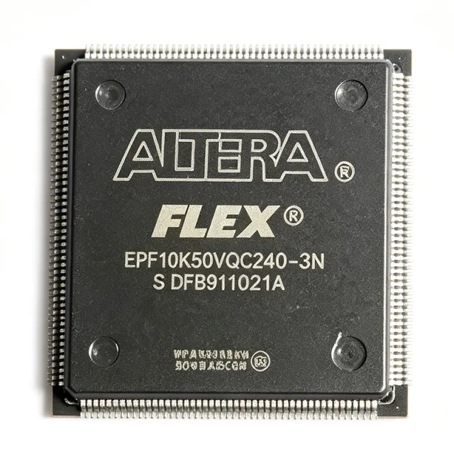
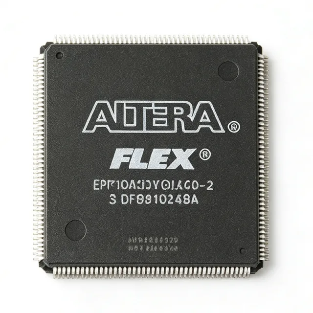
EPF10K50VRC240-2N
EPF10K50VRC240-2N - 50K-Gate FLEX 10K FPGA, 240-RQFP | Intel
The Intel EPF10K50VRC240-2N is a member of the FLEX 10K family of field-programmable gate arrays (FPGAs), delivering 50,000 typical gates, 2,880 logic elements/cells, and 360 logic array blocks (LABs) in a 240-pin RQFP (BFQFP with exposed pad) package. Operating from a 3.3 V supply with a 0.42 µm CMOS process and a maximum internal frequency of 125 MHz, this device targets commercial-temperature digital logic designs that need mid-range density, embedded array blocks (EABs) for RAM/ROM, and 189 user I/Os. The "V" suffix denotes the 3.3 V core supply variant, "RC" indicates the RQFP package, "240" is the pin count, "-2" is the speed grade, and the trailing "N" marks lead-free / Pb-free assembly.
An FPGA (Field-Programmable Gate Array) is a programmable logic device that lets engineers implement arbitrary digital logic - combinational gates, flip-flops, state machines, and memory blocks - by downloading a configuration bitstream after the IC is soldered onto the board. The FLEX 10K series was Intel/Altera's first generation to embed array blocks (EABs) for on-chip dual-port RAM, marking the industry's first System-on-a-Programmable-Chip (SOPC) integration. FPGAs sit hierarchically under programmable logic devices (PLDs), complex programmable logic devices (CPLDs), and finally the broader semiconductor / integrated circuit taxonomy.
Key features include 50,000 system gates, 20,480 flip-flop-based register bits, 2,880 logic elements, a maximum propagation delay of approximately 0.6 ns (66.67 MHz internal timing reference), 189 programmable I/O pins, four embedded array blocks (EABs) for distributed SRAM, JTAG-based IEEE 1149.1 boundary-scan testing, in-system programmability (ISP) via the serial passive configuration scheme, multi-volt I/O support (3.3 V core, 5.0 V-tolerant I/O), and a commercial 0 °C to 70 °C operating range. The exposed pad on the 240-RQFP package improves thermal dissipation during continuous logic switching.
The FLEX 10K architecture uses a row/column-based logic array, with each LAB containing eight logic elements (LEs), each LE built around a 4-input look-up table (LUT) plus a programmable flip-flop. EABs provide up to 2 Kbits of dual-port RAM each, allowing on-chip FIFOs, lookup tables, and small scratch-pad memories without external SRAM. Configuration is loaded from a serial EPROM or via the ByteBlaster / JTAG download cable in development flows, and the bitstream is held in SRAM cells so the device is re-programmable in the field an unlimited number of times.
Typical applications include custom glue logic in industrial control boards, PCI bridge and bus-interface controllers, telecommunications channel cards, prototyping of ASIC designs before mask production, DSP pre/post-processing pipelines, image processing front-ends, and embedded control subsystems. With 50K gates of usable logic, the EPF10K50VRC240-2N is well-suited to designs that need more capacity than a 10K30 device but do not yet justify the silicon cost of a 10K100 or 10K130.
When designing with the EPF10K50VRC240-2N, use the Quartus II (legacy) or MAX+PLUS II toolchain for synthesis, fitting, simulation, and programming file generation. Ensure clean 3.3 V core and I/O rail decoupling, observe the configuration mode wiring (MSEL pins), and respect JTAG chain order if multiple devices share the same boundary-scan bus. Because this device is in the legacy FLEX 10K family, plan for end-of-life (EOL) sourcing via franchised distributors or authorised aftermarket inventory.
This page synthesises franchised distributor pricing, same-package FLEX 10K drop-in alternatives, and practical design notes not consolidated in the legacy Altera datasheet.
Запрос цены
Контакты