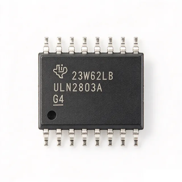
ULN2803ADWR - 8-Channel 50V 500mA Darlington Array | TI
Артикул: ULN2803ADWR ⚠ Последняя закупка| Кол-во | Цена за ед. | Итого |
|---|---|---|
| 1 | $0.95 | $0,95 |
| 10 | $0.82 | $8,20 |
| 100 | $0.65 | $65,00 |
| 500 | $0.52 | $260,00 |
| 1.000 | $0.44 | $440,00 |
| 2.000 | $0.38 | $760,00 |
ULN2803ADWR Обзор
A Darlington transistor array is an integrated circuit that combines multiple Darlington pairs - two bipolar transistors cascaded for very high current gain (hFE typically >1000) - into a single die. This category belongs to the power switch / load driver family within power-management semiconductors, sitting under the broader umbrella of discrete-array ICs. By integrating eight drivers, the part allows low-current logic outputs from microcontrollers, TTL, or CMOS gates to switch high-current loads with a minimum of external components.
Key features include 50 V continuous collector-emitter rating, 500 mA continuous collector current per channel (with peak inrush capability higher due to Darlington dynamics), 2.7 kOhm input base resistors allowing direct interface to 3.3 V and 5 V logic, and built-in flyback clamp diodes tied to COM. The -40 C to +85 C operating temperature range covers industrial environments. The 18-SOIC (DW) footprint is JEDEC-standard and footprint-compatible with several legacy through-hole-to-SMD migration designs.
Internally, each Darlington pair includes base and emitter resistors that set predictable turn-on thresholds and stabilize off-state leakage, while the integrated clamp diodes provide a defined current path for inductive kickback. Total package dissipation is bounded by thermal resistance; at 25 C ambient with adequate PCB copper, approximately 1.4 W is achievable. Output saturation voltage of about 1 V at rated current is the typical Darlington trade-off for high gain.
Typical applications include 5 V relay driver arrays, stepper motor winding drivers (commonly with bipolar stepper motors in 3D printers, CNC machines, and robotics), solenoid and valve drivers, LED and lamp matrix drivers, and logic-level buffers. The part directly interfaces MCU GPIO to high-current loads in a single SOIC-18 footprint, eliminating discrete transistor driver stages.
Always connect the COM pin (pin 10) to the positive supply of the inductive load so the clamp diodes can absorb back-EMF. Budget total package dissipation across all active channels and use adequate copper pour. This device is in Last Time Buy - consider drop-in alternatives below for new designs.
This page synthesizes distributor stock, drop-in alternatives, and practical design notes not consolidated in the manufacturer datasheet, helping engineers migrate from this LTB part with minimal PCB rework.
Аналоги без доработки для ULN2803ADWR — тот же корпус, pin-to-pin совместимость. Компоненты в других корпусах, требующие переработки PCB, исключены.
Варианты в этой серии
Модели той же серии, совместимые без доработки с ULN2803ADWR (тот же форм-фактор и посадочное место) — отличается по Package, Mounting Type, Clamp Diodes, Manufacturer, Operating Temperature Range.
Инструмент быстрого сравнения — выберите альтернативные компоненты для сравнения бок о бок:
ULN2803ADW
📋 Справочный аналог (нет в каталоге)
ULN2803APW
📋 Справочный аналог (нет в каталоге)
TD62083AFWG
📋 Справочный аналог (нет в каталоге)
A2982SLW
📋 Справочный аналог (нет в каталоге)
ULQ2803A
📋 Справочный аналог (нет в каталоге)
ULN2803ADWR Максимальные параметры и электрические характеристики
| Топология | 8-channel NPN Darlington array (sink driver) |
| Number of Channels | 8 |
| Collector-Emitter Voltage (VCEO max) | 50 V |
| Continuous Collector Current (per channel) | 500 mA |
| Input Base Resistor (per channel) | 2.7 kOhm |
| Output Clamp Diodes | 8 integrated, common-cathode to COM pin |
| Logic Compatibility | TTL / 5 V CMOS (also accepts 3.3 V) |
| Диапазон рабочих температур | -40 C to +85 C |
| Корпус | 18-SOIC (DW), 7.5 mm body width |
| Тип монтажа | Surface Mount |
| Уровень MSL | 1 (unlimited) |
| Lead-Free / RoHS | Yes / Compliant |
| Datasheet Document | ULN2803A datasheet (LRS049E family, revised July 2006 per TI) |
Конфигурация выводов ULN2803ADWR
| Контакт 1 | 1B — Channel 1 input (base) |
| Контакт 2 | 2B — Channel 2 input (base) |
| Контакт 3 | 3B — Channel 3 input (base) |
| Контакт 4 | 4B — Channel 4 input (base) |
| Контакт 5 | 5B — Channel 5 input (base) |
| Контакт 6 | 6B — Channel 6 input (base) |
| Контакт 7 | 7B — Channel 7 input (base) |
| Контакт 8 | 8B — Channel 8 input (base) |
| Контакт 9 | GND — Common emitter (ground return) |
| Контакт 10 | COM — Common cathode tie point for clamp diodes; connect to load positive supply |
| Контакт 11 | 8C — Channel 8 output (collector) |
| Контакт 12 | 7C — Channel 7 output (collector) |
| Контакт 13 | 6C — Channel 6 output (collector) |
| Контакт 14 | 5C — Channel 5 output (collector) |
| Контакт 15 | 4C — Channel 4 output (collector) |
| Контакт 16 | 3C — Channel 3 output (collector) |
| Контакт 17 | 2C — Channel 2 output (collector) |
| Контакт 18 | 1C — Channel 1 output (collector) |
Типичное применение
ULN2803ADWR подходит для 6 применениеs: 5V Relay Driver Array, Bipolar Stepper Motor Driver, Solenoid and Valve Driver Array, LED Matrix and Display Driver, Logic Buffer / Level Shifter, Hammer Driver / Dot Matrix Printer.
5V Relay Driver Array
The ULN2803ADWR is widely used as a 5 V relay driver array for industrial control boards, HVAC systems, and home automation where eight or fewer SPDT relays must be driven from a low-current MCU GPIO bank. Each channel's 500 mA continuous collector current comfortably drives most signal relays (typical coil current 20-70 mA), while the 50 V VCEO rating exceeds the inductive kickback of any common 5 V, 12 V, or 24 V relay coil when paired with the integrated clamp diode tied to COM (pin 10). The 2.7 kOhm base resistors accept 3.3 V MCU outputs directly without level shifters. PCB copper pour is recommended because total package dissipation rises when all eight relays are energized simultaneously.
Рекомендуется
Bipolar Stepper Motor Driver
In 3D printers, CNC machines, robotics, and small CNC routers, two ULN2803ADWR devices commonly form the low-side driver pair for a bipolar stepper motor (one ULN2803ADWR for phase A windings, a second for phase B). Each channel's 500 mA collector current supports stepper phase currents up to that value per phase (1.4 A peak per phase with two channels paralleled), while the 50 V VCEO rating handles the inductive back-EMF of typical 12 V to 24 V bipolar stepper windings. The clamp diodes tied to COM provide a defined flyback path, eliminating the need for external freewheel diodes. The TTL-compatible inputs accept step/direction pulses directly from a 3.3 V or 5 V MCU.
Рекомендуется
Solenoid and Valve Driver Array
Pneumatic and hydraulic solenoid valves in industrial automation typically draw 100-300 mA per coil at 12 V or 24 V, well within the ULN2803ADWR's 500 mA per-channel rating. The part's 50 V collector-emitter rating gives ample margin for the inductive flyback of typical 24 V solenoid coils when the integrated clamp diodes (tied to COM at the load supply rail) absorb the energy. Each channel can sink the inrush current of direct-acting solenoid valves and the holding current of pilot-operated valves. Eight channels per package make the ULN2803ADWR efficient for multi-valve manifolds in factory automation PLCs and process-control equipment.
Рекомендуется
LED Matrix and Display Driver
The ULN2803ADWR is commonly used as a column (cathode) driver in small LED matrices, seven-segment multiplexed displays, and bar-graph indicators where each channel sinks up to 500 mA. Eight channels per package align naturally with 8-column dot-matrix displays and 8-digit seven-segment common-cathode arrangements. The 2.7 kOhm base resistors accept 3.3 V or 5 V logic directly from display controller ICs, while the integrated clamp diodes allow safe driving of multiplexed LED arrays without external protection. Designers should budget average current per channel (not peak) to stay within thermal limits, since LED matrices pulse-modulate each column at high duty cycle.
Рекомендуется
Logic Buffer / Level Shifter
When a low-current logic output (such as a 3.3 V MCU GPIO rated at 4-20 mA) must drive a higher-current load that exceeds the GPIO's direct-drive capability, the ULN2803ADWR provides 8 channels of current amplification in a single SOIC-18 package. Each Darlington pair offers a DC current gain typically above 1000, meaning a 1 mA base current can sink 500 mA at the collector. The 2.7 kOhm input resistors limit base current to a safe value while still allowing direct drive from 3.3 V GPIO. This makes the ULN2803ADWR a common building block in legacy industrial logic interface boards and test equipment where 5 V or 12 V signals must be switched under MCU control.
Рекомендуется
Hammer Driver / Dot Matrix Printer
In legacy dot-matrix printer head designs and similar hammer-driver applications (solenoid actuators, ticket dispensers), the ULN2803ADWR provides eight high-current sink channels that can pulse-magnetic hammer coils at high repetition rates. Each channel's 500 mA continuous rating handles the average coil current, while the integrated clamp diodes absorb the inductive kickback generated when each hammer is released. The 50 V VCEO rating supports 24 V or 36 V hammer coil supplies common in industrial printing. The 18-SOIC package allows dense PCB layouts where eight or more driver channels must fit on a small printer-controller board.
Рекомендуется
Сводка рекомендуемых товаров
Справочные инженерные данные для ULN2803ADWR — сравнение, рекомендации по проектированию и информация о соответствии.
Руководство по выбору
Сравнение с аналогами
| Параметр | Этот товар | ULN2803ADW | ULN2803APW | TD62083AFWG | A2982SLW | ULQ2803A |
|---|---|---|---|---|---|---|
| Brand | Texas Instruments | Texas Instruments | Texas Instruments | Toshiba | Allegro MicroSystems | Microchip Technology |
| Package | 18-SOIC (DW), 7.5 mm body | 18-SOIC (DW), 7.5 mm body - same | 18-TSSOP (PW), 6.4 mm body - smaller | 18-SOIC (DW), 7.5 mm body - same | 18-SOIC (DW), 7.5 mm body - same | 18-SOIC (DW), 7.5 mm body - same |
| Number of Channels | 8 | 8 | 8 | 8 | 8 | 8 |
| VCEO Maximum | 50 V | 50 V | 50 V | 50 V | 50 V | 50 V |
| Continuous Collector Current | 500 mA per channel | 500 mA | 500 mA | 500 mA | 500 mA | 500 mA |
| Input Base Resistor | 2.7 kOhm | 2.7 kOhm | 2.7 kOhm | 2.7 kOhm | 2.7 kOhm | 2.7 kOhm |
| Integrated Clamp Diodes | Yes (8x, tied to COM pin) | Yes | Yes | Yes | Yes | Yes |
| Operating Temperature | -40 C to +85 C | -40 C to +85 C | -40 C to +85 C | -40 C to +85 C | -40 C to +85 C | -40 C to +125 C (automotive) |
| Lifecycle Status | Last Time Buy | Last Time Buy | Active | Active | Active | Active |
| Approx. Unit Price (qty-1000) | $0.44 | $0.44 (tray variant) | $0.48 | $0.55 | $0.85 | $0.95 |
Ключевые отличия
- Industry-standard pinout with broadest cross-brand support (против TD62083AFWG)
- Same-family TSSOP variant available for compact layouts (против ULN2803APW)
- Lower cost at production volumes vs. Allegro equivalent (против A2982SLW)
Заметки по проектированию
Estimated: at VCE(sat) ~1.0 V and 500 mA load on a single channel, the dissipation per channel is ~0.5 W. With all eight channels active simultaneously at rated current, total package dissipation reaches ~4 W, well beyond the 18-SOIC's safe operating area of ~1 W continuous at 25 C ambient without copper pour. For multi-channel continuous operation, designers must either reduce per-channel current, parallel fewer channels at a time, or use substantial PCB copper pour plus airflow to spread the heat. Thermal resistance theta_JA for SOIC-18 is approximately 70 C/W on a standard JEDEC test board.
Always connect pin 10 (COM) to the positive supply that powers the inductive loads - typically the same rail as the load's V+. Without COM connected, the integrated clamp diodes have no return path and inductive kickback will exceed the 50 V VCEO rating, destroying one or more outputs. Place a small bulk capacitor (10-100 uF electrolytic plus 100 nF ceramic) near the COM pin to absorb the clamp-diode return currents. Keep the COM trace short and wide to handle transient currents during inductive switching.
Three common design pitfalls: (1) forgetting to connect the COM pin, which destroys outputs when switching inductive loads; (2) exceeding total package dissipation by driving all eight channels at full rated current simultaneously - in practice derate to 60-70% per channel; (3) assuming 3.3 V logic cannot drive the part - the 2.7 kOhm input resistor with Darlington VBE ~1.2 V still allows sufficient base current at 3.3 V to saturate the output. Also note that channels can be paralleled (connect inputs together, outputs together) for higher current but this reduces channel count.
Use a copper pour under and around the 18-SOIC footprint to spread heat; without it, theta_JA can exceed 100 C/W and the part will thermally limit at much lower than rated current. Place input traces on the top side of the board (corresponding to pins 1-8) and output traces on the bottom side (pins 11-18) for cleanest routing. Keep analog/digital ground separate if the ULN2803ADWR is switching near sensitive analog circuits - the shared GND pin (pin 9) carries the return current of all eight channels.
Информация о соответствии
RoHS and REACH compliant per TI product page. Lead-free (Pb-free) reflow-compatible. Standard -40 C to +85 C industrial grade; not AEC-Q100 qualified - use the ULQ2803A (Microchip) for AEC-Q100 automotive applications. Halogen-free per TI declaration.







