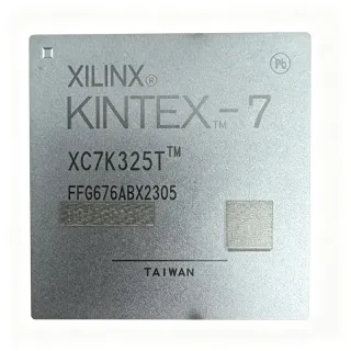
XC5VLX85-2FF676I - 85K Virtex-5 LX FPGA | AMD
Артикул: XC5VLX85-2FF676I ✗ Снят с производстваXC5VLX85-2FF676I Обзор
A field-programmable gate array is a semiconductor device whose digital logic, interconnect, and I/O behavior are configured after manufacture. The FPGA category sits above programmable logic devices and forms part of the broader semiconductor and embedded-processing ecosystem. Compared with a fixed-function application-specific integrated circuit, an FPGA supports design changes, parallel processing, custom interfaces, and hardware acceleration without requiring a new ASIC fabrication run. The Virtex-5 LX family uses AMD's second-generation ASMBL column-based architecture.
The XC5VLX85-2FF676I combines 3,538,944 logic cells, 82,944 register bits, and 440 I/O in one high-pin-count package. These figures make the device suitable for systems requiring considerable parallel logic, multiple high-speed interfaces, substantial data movement, or adaptable control paths. The -2 speed designation identifies a specific performance grade, while the industrial temperature designation supports designs intended to operate across an extended environmental range when the complete system and board-level requirements are also satisfied.
The large 676-ball FCBGA footprint exposes substantially more device connections than a typical leaded FPGA package. That interface density can support wide parallel buses, multiple I/O standards, dedicated memory interfaces, clocks, and high-speed differential pairs. Because package escape routing, power delivery, and ball-assignment constraints become more demanding at this density, the device should be designed using the manufacturer’s pinout, package information, and board-design guidance rather than inferred from a generic BGA symbol.
Typical uses include industrial control and automation, communications infrastructure, test and measurement equipment, embedded instrumentation, video processing, and high-throughput data-acquisition systems. Its 440 available I/O can accommodate multiple external interfaces, while the 85K-scale logic fabric can implement parallel algorithms, protocol engines, control logic, and signal-processing pipelines. Industrial temperature grading is particularly relevant to equipment that must operate reliably beyond typical consumer-environment limits.
The main design consideration is that a 676-ball FPGA requires disciplined power-plane segmentation, decoupling, ball-grid layout work, and careful high-speed routing. Designers should preserve the pin and bank functions required by the design, validate every I/O standard against the selected bank, and use the manufacturer’s recommended configuration and power-sequencing procedures. Migration to another device should not be treated as automatic even when logic resources and package names appear similar.
This product page organizes the verified device identity, package details, commercial inquiry path, comparison points, and engineering guidance around the XC5VLX85-2FF676I. It also distinguishes true package-compatible family options from broader FPGA redesign alternatives, helping teams evaluate replacement risk before committing to a new PCB or bitstream.
Аналоги без доработки для XC5VLX85-2FF676I — тот же корпус, pin-to-pin совместимость. Компоненты в других корпусах, требующие переработки PCB, исключены.
Варианты в этой серии
Модели той же серии, совместимые без доработки с XC5VLX85-2FF676I (тот же форм-фактор и посадочное место) — отличается по Device Type, RoHS Status, Speed Grade.
XC5VLX85-2FFG676I
✅ Прямая замена📋 Справочный аналог (нет в каталоге)
XC5VLX85-3FF676C
✅ Прямая замена📋 Справочный аналог (нет в каталоге)
XC5VLX110-2FF676I
✅ Прямая замена📋 Справочный аналог (нет в каталоге)
XC5VLX85-2FF676I Максимальные параметры и электрические характеристики
| Device Type | Virtex-5 LX Field Programmable Gate Array (FPGA) |
| Logic Cells | 3,538,944 |
| Register Bits | 82,944 |
| Number of I/O | 440 |
| Architecture | Second-generation ASMBL column-based architecture |
| Speed Grade | -2 |
| Temperature Grade | Industrial |
| Package Type | 676-BBGA, FCBGA |
| Number of Terminals | 676 |
| Terminal Form | Ball |
| Package Shape | Square |
| Тип монтажа | Surface Mount |
| Lead-Free Status | Contains Lead |
| Статус RoHS | RoHS Non-Compliant |
| Programmable Logic Type | FPGA |
| Product Family | Virtex-5 LX |
| Manufacturer | AMD |
Руководство по цоколевке XC5VLX85-2FF676I в корпусе square
Цоколевка для XC5VLX85-2FF676I (корпус square). Эта цифровая ИС включает выводы GPIO, интерфейсы связи (UART, SPI, I2C) и выводы питания. Обратитесь к техническому описанию производителя для альтернативных функций выводов и вариантов конфигурации. Необходимо для проектирования встраиваемых систем и трассировки печатных плат.

Нет подробных данных о распиновке для XC5VLX85-2FF676I.
Обратитесь к даташиту для полной конфигурации выводов.
Типичное применение
XC5VLX85-2FF676I подходит для 6 применениеs: Industrial Automation and Control, Communications and Network Interface, Test and Measurement Systems, Video and Image Processing, Data Acquisition and Signal Processing, High-Performance Embedded Processing.
Industrial Automation and Control
The XC5VLX85-2FF676I fits factory automation controllers that combine deterministic parallel control with multiple external interfaces. Its 3,538,944 logic cells can support sequencing, state machines, protocol handling, diagnostics, and supervisory logic, while 440 I/O provide connectivity to sensors, actuators, motor stages, and operator panels. The industrial-temperature grade is relevant to equipment operating in variable ambient conditions. Engineers should use the manufacturer bank rules to assign external standards to compatible I/O pins, preserve required configuration pins, and decouple each supply group according to the Virtex-5 power architecture.
Рекомендуется
Communications and Network Interface
The XC5VLX85-2FF676I is suitable for line cards, protocol converters, packet-processing modules, and communications test equipment that need a large amount of parallel programmable logic. The 85K-scale fabric can implement framing engines, CRC logic, buffers, scheduling functions, and multiple interface channels, while 440 I/O support wide data buses and differential I/O. The -2 grade provides a defined speed option, and the industrial suffix supports extended-temperature equipment. Design work should include exhaustive static timing analysis and careful assignment of clock-capable, voltage-reference, and general-purpose pins within the 676-ball package.
Рекомендуется
Test and Measurement Systems
For oscilloscopes, logic analyzers, data-acquisition platforms, and automated test equipment, the XC5VLX85-2FF676I can combine acquisition control, trigger processing, pattern generation, and data reduction in one programmable device. The 3,538,944 logic cells accommodate parallel channels and sophisticated timing logic, while 440 I/O reduce the need for external multiplexing in moderately complex systems. The industrial grade can suit laboratory and production equipment with controlled thermal environments. Engineers should use the manufacturer’s supported clocking and I/O standards and verify acquisition timing against the -2 device speed characteristics.
Рекомендуется
Video and Image Processing
The XC5VLX85-2FF676I can implement parallel image pipelines, pixel manipulation, color processing, frame timing, and interface bridging. Its 85K-scale logic fabric supports concurrent processing stages, while 440 I/O provide substantial connectivity for parallel sensors, memory interfaces, and downstream processors. The -2 speed grade is appropriate for designs requiring more timing margin than a lower or differently graded device. Layout engineers must plan high-speed data routing carefully in the 676-ball FCBGA, maintain continuous return paths, and apply the manufacturer’s guidance for I/O standards and clocking.
Рекомендуется
Data Acquisition and Signal Processing
The XC5VLX85-2FF676I is well suited to multichannel acquisition, digital filtering, correlation, real-time analysis, and sensor fusion. Its 3,538,944 logic cells support parallel arithmetic and control pipelines, while 82,944 register bits provide state storage and 440 I/O support converters, transducers, memory, and synchronization signals. The industrial-temperature option benefits deployed instrumentation and factory data loggers. Signal-integrity planning should include controlled clock distribution, matched data-bus lengths where required, separate analog and digital power regions, and validation of every high-speed interface against the device bank characteristics.
Рекомендуется
High-Performance Embedded Processing
The XC5VLX85-2FF676I can serve as a hardware accelerator or co-processor alongside a host processor, offloading filtering, compression, encryption, or protocol workloads. The 85K-class fabric allows multiple parallel pipelines to operate concurrently, and the 440 I/O provide flexible integration with processors, memory, and external accelerators. Its industrial-temperature designation supports embedded equipment with constrained thermal environments. Because large FPGAs can demand substantial power and routing resources, engineers should evaluate resource utilization, timing closure, configuration storage, and thermal margins before finalizing the processor split and board power design.
Рекомендуется
Справочные инженерные данные для XC5VLX85-2FF676I — сравнение, рекомендации по проектированию и информация о соответствии.
Руководство по выбору
Сравнение с аналогами
| Параметр | Этот товар | XC5VLX85-2FFG676I | XC5VLX85-3FF676C | XC5VLX110-2FF676I |
|---|---|---|---|---|
| Package | 676-BBGA, FCBGA | 676-BBGA, FCBGA | 676-BBGA, FCBGA | 676-BBGA, FCBGA |
| Brand | AMD | AMD | AMD | AMD |
| Device Family | Virtex-5 LX | Virtex-5 LX | Virtex-5 LX | Virtex-5 LX |
| Speed Grade | -2 | -2 | -3 | -2 |
| Temperature Grade | Industrial | Industrial | Commercial | Industrial |
| Architecture | Second-generation ASMBL column-based architecture | Virtex-5 second-generation ASMBL column-based architecture | Virtex-5 second-generation ASMBL column-based architecture | Virtex-5 second-generation ASMBL column-based architecture |
| Terminal Count | 676 | 676 | 676 | 676 |
Ключевые отличия
- Higher speed grade than the identified -3 family option (против XC5VLX85-3FF676C)
- Industrial temperature grade (против XC5VLX85-3FF676C)
- Exact 85K device-size positioning (против XC5VLX110-2FF676I)
Заметки по проектированию
Implement the Virtex-5 recommended power architecture with separate supply rails where required by the device configuration. Place bulk and high-frequency decoupling capacitors close to their assigned package balls, preserve the recommended power-plane connectivity, and control sequencing across supply groups. Do not estimate rail requirements from generic FPGA experience alone; use the exact device power table and board-design guide for XC5VLX85-2FF676I.
Plan the 676-ball FCBGA escape routing and complete ball-assignment check before schematic release. Match pin functions to the exact ordering code and package revision, retain clock-capable and voltage-reference assignments, and route high-speed differential pairs with continuous reference planes. A package name match does not prove ball-for-ball compatibility between ordering-code variants.
Use the manufacturer’s I/O-standard and bank rules to select voltage, slew, and drive settings. Keep clocks on appropriate clock-capable pins, route source-synchronous interfaces with matched data and strobe topology, and include series termination where the I/O standard and board environment require it. Validate edge quality and timing at the -2 speed grade rather than relying only on functional simulation.
Do not treat the XC5VLX85, XC5VLX110, or different speed and temperature suffixes as unconditional substitutions. The XC5VLX85-3FF676C changes both speed and thermal grade, while XC5VLX110 changes device resources. Confirm lifecycle requirements, I/O assignments, timing, power, configuration behavior, and qualification, then rebuild and rerun all timing and hardware tests before production use.
Информация о соответствии
The product data identifies the device as containing lead and RoHS non-compliant. No qualifying information was available for REACH, halogen-free status, or conflict-minerals compliance.