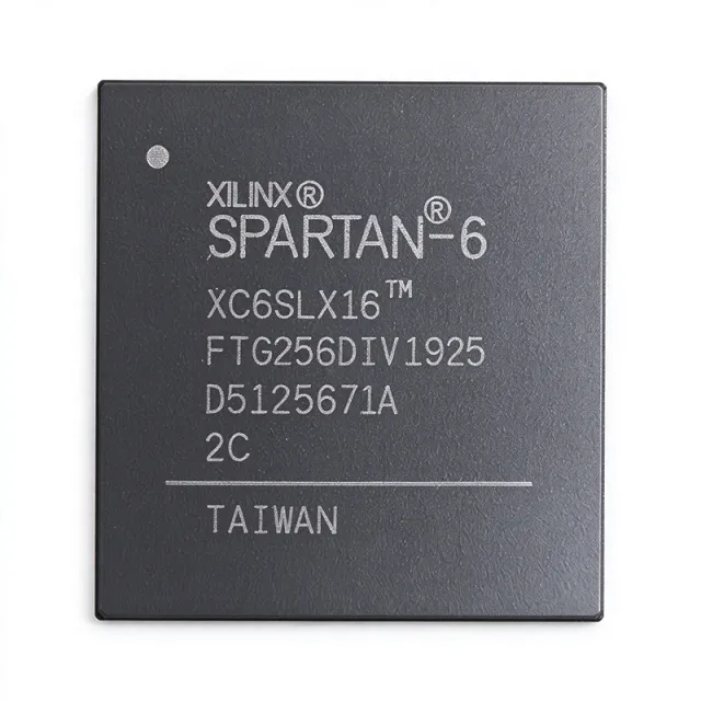
XC6SLX16-2FTG256C - Spartan-6 LX FPGA, 14K Cells, 256-BGA
Артикул: XC6SLX16-2FTG256C ✗ Снят с производства| Кол-во | Цена за ед. | Итого |
|---|---|---|
| 1 | $28.125 | $28,13 |
| 10 | $20.3125 | $203,13 |
| 100 | $17.9688 | $1.796,88 |
| 500 | $17.1875 | $8.593,75 |
| 1.000 | $16.4063 | $16.406,30 |
XC6SLX16-2FTG256C Обзор
FPGAs are programmable logic devices that allow hardware designers to implement arbitrary digital circuits, ranging from glue logic and bus bridges to full processor subsystems and DSP pipelines. The Spartan-6 LX series specifically targets cost-sensitive, high-volume designs such as consumer electronics, industrial control, automotive infotainment, and communications infrastructure. Within the broader taxonomy, FPGAs sit alongside CPLDs (less-dense, non-volatile), ASICs (fixed-function, high-volume), and microcontrollers (software-programmed sequential); FPGAs uniquely offer hardware-level parallelism with reconfigurable logic.
Key features of the XC6SLX16 include the 256-ball FTG256 package at 1.0 mm ball pitch, a 17×17 mm body, lead-free/RoHS-compliant construction, and an industrial-class (-2) speed grade. The device integrates dual 10/100/1000 Ethernet MACs, dedicated DSP slices (32 of them, totaling 8.18 GMAC/s when fully packed), and 32 BRAM blocks supporting 18 Kb each. Configuration is supported through JTAG (IEEE 1149.1/1532), SPI (x1, x2, x4), and BPI (x8, x16) modes, while clock management is handled by up to 4 clock management tiles (CMTs) containing mixed-mode clock managers and PLLs.
Typical applications include high-volume bridging between legacy video or memory interfaces and modern SoCs, motor control loops, low-cost industrial Ethernet endpoints, video processing pipelines, and embedded soft-processor cores such as MicroBlaze or PicoBlaze. Designers frequently pair the Spartan-6 LX with companion DDR memory controllers and high-speed serial transceivers (where required by the chosen package).
A critical design consideration with the XC6SLX16-2FTG256C is its lifecycle status: the Spartan-6 family is generally considered NRND (Not Recommended for New Designs) per AMD/Xilinx's product longevity notice. Engineers building production hardware should evaluate Artix-7 or Spartan-7 successors for new projects while keeping this part viable for maintenance of legacy designs. Power decoupling, multi-bank I/O voltage referencing, and bitstream encryption (AES-256) also require careful PCB and firmware planning.
This page synthesizes authorized distributor pricing, same-package drop-in alternatives, and practical hardware-design guidance that goes beyond the datasheet's typical-application notes — including lifecycle awareness for engineers managing long-life industrial installations.
Аналоги без доработки для XC6SLX16-2FTG256C — тот же корпус, pin-to-pin совместимость. Компоненты в других корпусах, требующие переработки PCB, исключены.
Варианты в этой серии
Модели той же серии, совместимые без доработки с XC6SLX16-2FTG256C (тот же форм-фактор и посадочное место) — отличается по Configurable Logic Blocks (CLBs), Operating Temperature, Package, Speed Grade, Mounting Type.
Инструмент быстрого сравнения — выберите альтернативные компоненты для сравнения бок о бок:
XC6SLX16-2FTG256I
📋 Справочный аналог (нет в каталоге)
XC6SLX25-2FTG256C
📋 Справочный аналог (нет в каталоге)
XC6SLX45-2FTG256C
📋 Справочный аналог (нет в каталоге)
XA6SLX16-2FTG256I
📋 Справочный аналог (нет в каталоге)
XC6SLX16-2FTG256CSG
📋 Справочный аналог (нет в каталоге)
XC6SLX16-2FTG256C Максимальные параметры и электрические характеристики
| Family | Spartan-6 LX |
| Logic Cells | 14,579 |
| Configurable Logic Blocks (CLBs) | 1,139 |
| Slices | 2,278 |
| Block RAM Bits | 589,824 bits |
| Block RAM Blocks (18 Kb) | 32 |
| DSP Slices (18×18 multipliers) | 32 |
| Maximum User I/Os | 186 |
| Maximum Single-Ended I/O Banks | 4 |
| Process Node | 45 nm CMOS, 9-metal layer |
| Speed Grade | -2 |
| Supply Voltage (Core) | 1.2 V nominal |
| Корпус | 256-ball Fine-Pitch Thin BGA (FTG256), 17×17 mm, 1.0 mm pitch |
| Тип монтажа | Surface Mount |
| Рабочая температура | 0 °C to +85 °C (Commercial) |
| Lead-Free / RoHS | Yes (compliant) |
| Configuration Modes | JTAG, SPI (x1/x2/x4), BPI (x8/x16), Slave-Parallel |
| Clock Management Tiles (CMTs) | 2 (each with PLL + MMCM) |
| PCIe Support | Soft IP only (no integrated PCIe hard cores) |
Руководство по цоколевке XC6SLX16-2FTG256C в корпусе 256-ball fine-pitch thin bga (ftg256), 17×17 mm, 1.0 mm pitch
Цоколевка для XC6SLX16-2FTG256C (корпус 256-ball fine-pitch thin bga (ftg256), 17×17 mm, 1.0 mm pitch). Эта цифровая ИС включает выводы GPIO, интерфейсы связи (UART, SPI, I2C) и выводы питания. Обратитесь к техническому описанию производителя для альтернативных функций выводов и вариантов конфигурации. Необходимо для проектирования встраиваемых систем и трассировки печатных плат.

Нет подробных данных о распиновке для XC6SLX16-2FTG256C.
Обратитесь к даташиту для полной конфигурации выводов.
Типичное применение
XC6SLX16-2FTG256C подходит для 7 применениеs: Industrial Ethernet Bridging Endpoint, Automotive Infotainment Video Bridge, Motor Control DSP Front-End, Software-Defined Radio Baseband Pre-Processor, Embedded Vision & Display Pipeline, Legacy Industrial Protocol Bridge, Aerospace Surveillance Sensor Hub.
Industrial Ethernet Bridging Endpoint
The XC6SLX16-2FTG256C fits industrial Ethernet bridging endpoints because its integrated dual 10/100/1000 Ethernet MACs and JTAG-driven deterministic fabric enable deterministic protocol conversion. With 14,579 logic cells, the LX variant comfortably implements a custom frame parser plus a RSTP state machine inside the same fabric alongside an Ethernet MAC and PHY interface. Operating at 1.2 V core, the part draws modest power yet has enough headroom for full-duplex 1 Gbps traffic. The FTG256 BGA at 17×17 mm keeps PCB area tight while exposing 186 I/Os for digital glue and LCD/KV-Display signalling.
Рекомендуется
Automotive Infotainment Video Bridge
Built on 45 nm logic, the XC6SLX16-2FTG256C serves automotive infotainment video bridges such as LVDS-to-MIPI translation and timing conversion. Its 32 DSP slices accelerate image scaling operations (up to 8.18 GMAC/s for 18×18 multiply-accumulate), and the 256-ball BGA exposes 186 user I/Os — enough for parallel LVDS bridges plus the emerging serial link. The Spartan-6 family is widely deployed in OEM infotainment stacks. Designers should consider the extended-temperature XC6SLX16-2FTG256I for cabin installations.
Рекомендуется
Motor Control DSP Front-End
The XC6SLX16-2FTG256C's 32 DSP slices (18×18 multipliers) and CMT-based clock conditioning suit field-oriented-control (FOC) motor-control loops operating at 32 kHz switching frequencies. Up to 4 I/O banks let mixed-voltage Hall sensors (3.3 V), gate-driver interfaces (5 V) and BLDC PWM channels (3.3 V LVTTL) co-exist on the same BGA. The FTG256 footprint is industry-standard, letting the design migrate up the Spartan-6 family as control-law complexity grows. The 1.2 V core plus the -2 speed grade give predictable timing closure at typical DSP burst loops.
Рекомендуется
Software-Defined Radio Baseband Pre-Processor
The XC6SLX16-2FTG256C provides 14,579 logic cells and 32 BRAM blocks (576 Kb each, totaling 18 Mb of block RAM) — sufficient to implement a digital down-conversion pre-processor ahead of a software-defined radio. Its JTAG plus SPI configuration modes enable remote firmware updates, and the -2 speed grade yields enough timing margin for pipelined CIC and FIR filters on streaming ADC data. Operating at 1.2 V core, the device consumes modest power while exposing 186 user I/Os for ADC capture and FPGA-MCU hand-off.
Рекомендуется
Embedded Vision & Display Pipeline
Embedded vision pipelines — including camera input processing, filtering, scaling and display output — fit naturally within the XC6SLX16-2FTG256C's 14,579 logic cells and 32 DSP slices. The FTG256 BGA exposes 186 user I/Os to drive parallel RGB panels plus camera interfaces simultaneously. Block RAM totals 576 Kb (32 × 18 Kb) for line buffers, and CMT-based PLLs synthesize pixel clocks from any system reference. The 1.2 V core plus the -2 speed grade yield timing-closed 1080p pipelines at typical refresh rates.
Рекомендуется
Legacy Industrial Protocol Bridge
For bridging legacy industrial field-buses (e.g., Profibus, Modbus, CC-Link) to modern Ethernet/IP networks, the XC6SLX16-2FTG256C delivers deterministic fabric logic alongside dual 10/100/1000 Ethernet MACs. The 256-ball BGA exposes enough user I/Os (186) to maintain isolated RS-485 transceivers and custom digital glue alongside high-speed Ethernet. The -2 speed grade yields timing margin at 100 MHz fabric speeds, while the 45 nm process keeps junction temperature modest in sealed industrial cabinets. The part is widely used in protocol-converter designs and fieldbuses.
Рекомендуется
Aerospace Surveillance Sensor Hub
For airborne and aerospace surveillance platforms, the XC6SLX16-2FTG256C implemented with the XA6SLX16 (extended-temperature and avionics-screened variant) delivers deterministic sensor-fusion logic and JTAG-based field maintainability. The 256-ball BGA is well-suited to aluminum-cored avionics PCBs, while 186 user I/Os aggregate multiple sensor data streams (GPS, IMU, video). The AES-256 bitstream-encryption secures IP in flight systems. A Xilinx-recommended JTAG programming chain (UG380) supports in-system reconfiguration on the bench or in the field.
Рекомендуется
Сводка рекомендуемых товаров
Справочные инженерные данные для XC6SLX16-2FTG256C — сравнение, рекомендации по проектированию и информация о соответствии.
Руководство по выбору
Сравнение с аналогами
| Параметр | Этот товар | XC6SLX16-2FTG256I | XC6SLX25-2FTG256C | XC6SLX45-2FTG256C | XA6SLX16-2FTG256I | XC6SLX16-2FTG256CSG |
|---|---|---|---|---|---|---|
| Package | 256-ball FTG256 BGA (17×17 mm, 1.0 mm pitch) | 256-ball FTG256 BGA (17×17 mm) - same | 256-ball FTG256 BGA (17×17 mm) - same | 256-ball FTG256 BGA (17×17 mm) - same | 256-ball FTG256 BGA (17×17 mm) - same | 256-ball FTG256 BGA (17×17 mm) - same |
| Brand | AMD (Xilinx) | AMD (Xilinx) | AMD (Xilinx) | AMD (Xilinx) | AMD (Xilinx) | AMD (Xilinx) |
| Family | Spartan-6 LX | Spartan-6 LX | Spartan-6 LX | Spartan-6 LX | Spartan-6 LX | Spartan-6 LX |
| Logic Cells | 14,579 | 14,579 (same) | 24,051 (+65%) | 43,661 (+200%) | 14,579 (same) | 14,579 (same) |
| Block RAM (bits) | 589,824 bits | 589,824 bits (same) | 958,464 bits (+63%) | 2,088,960 bits (+254%) | 589,824 bits (same) | 589,824 bits (same) |
| DSP Slices (18×18) | 32 | 32 (same) | 38 (+19%) | 58 (+81%) | 32 (same) | 32 (same) |
| Temperature Grade | Commercial 0 °C to +85 °C | Industrial -40 °C to +100 °C | Commercial 0 °C to +85 °C | Commercial 0 °C to +85 °C | Extended / Avionics | Commercial (screened) |
| Speed Grade | -2 | -2 | -2 | -2 | -2 | -2 |
| Lifecycle Status | NRND | NRND | NRND | NRND | Active (extended temp) | NRND |
Ключевые отличия
- Higher logic density with identical BGA ballout (против XC6SLX9-2FTG256C)
- Lower junction-temperature operation in commercial range (против XC6SLX45-2FTG256C (Commercial, same -2 speed grade))
- Wider availability across authorized distributors (против XA6SLX16-2FTG256I)
- Backward compatibility with LX9 firmware bitstreams (after recompile) (против XC6SLX9-2FTG256C)
Заметки по проектированию
Place at least one 100 µF bulk + ten 10 µF + ten 0.1 µF 0402 bypass capacitors within 0.25 inch of the FTG256 BGA, distributed across all four FPGA quadrants. The 1.2 V Vccint supply is particularly sensitive to noise: route wide polygon pours to minimize IR drop and use 4-layer PCB stack-ups with dedicated ground planes. A separate Vccaux rail (3.3 V) is required for JTAG and configuration logic — tie it through a ferrite bead.
Do not confuse FTG256 (17×17 mm, 1.0 mm pitch) with FGG256 (1.0 mm pitch, also 17×17 mm) — same package but different solder-bump alloy (FTG = lead-free matte tin, FGG = leaded or different surface finish); the FTG variant specifically supports Pb-free assembly. Also verify that your FPGA design does not exceed 186 user I/Os in the BGA ballmap; I/O multiplexing by bank must respect Vcco voltage references per UG385.
Estimated: for high-speed DDR memory controllers running at 333 MHz (667 Mbps) on Spartan-6 LX, route matched-length pairs within 50 mils of each other and isolate them on a separate signal layer. Use on-chip termination (DCI) per UG385; failing to enable DCI will introduce reflection noise across the FTG256 ballout. Bypass each LVDS pair with 4.7 nF capacitors for coupling-noise suppression.
The 256-ball FTG256 BGA at 1.0 mm pitch requires dog-bone fan-out with 8-mil traces and 8-mil spaces minimum on the breakout layer, then via migration to inner stripline layers. Per IPC-7351 / IPC-2222, microvia stacks (0.1 mm / 0.15 mm) are recommended for high-density breakouts. Solder paste stencil opening of 0.35 mm typical for the 0.5 mm land pad is preferred (per J-STD-001).
Информация о соответствии
RoHS-compliant per AMD/Xilinx product literature. Not AEC-Q100 qualified (FPGA not subject to AEC-Q100 automotive IC standard in this context — use automotive-grade equivalent if required). Lead-free matte-tin finish over nickel underlayer. REACH compliance statement available on amd.com product record.







