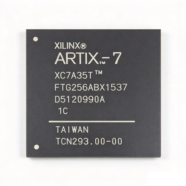
XC7A35T-1FTG256C - Artix-7 FPGA, 33K Logic Cells | AMD Xilinx
Артикул: XC7A35T-1FTG256C ✓ Активен| Кол-во | Цена за ед. | Итого |
|---|---|---|
| 1 | $142.5 | $142,50 |
| 10 | $128.75 | $1.287,50 |
| 100 | $112.4 | $11.240,00 |
| 500 | $96.85 | $48.425,00 |
| 1.000 | $84.2 | $84.200,00 |
XC7A35T-1FTG256C Обзор
An FPGA (Field Programmable Gate Array) is a semiconductor integrated circuit whose digital logic, interconnect, and I/O behavior are configured by the user after manufacture via a hardware description language (HDL) bitstream. FPGAs sit in the broader taxonomy of programmable logic devices alongside CPLDs and are widely used for parallel DSP, custom I/O protocols, and rapid prototyping where ASIC NRE costs are unjustified. The Artix-7 family is positioned as the low-power, cost-optimized member of the Xilinx 7-Series, between the high-performance Virtex-7 and the lower-cost Spartan-6 predecessors.
Key features include four GTP transceivers supporting up to 6.6 Gb/s line rates (artix-7 35T family), 5 MMCM/PLL clock management tiles, an integrated 12-bit 1 Msps XADC analog-to-digital converter, and on-chip configuration memory supporting multiple boot modes including SPI, BPI, JTAG, and Master/Slave SelectMAP. The Artix-7 35T variant specifically adds the 4 GTP serial transceivers that the smaller 15T and non-T parts omit.
Typical applications include software-defined radio (SDR) leveraging the 90 DSP slices for high-performance modulation and filtering, machine vision and industrial imaging pipelines using parallel sensor interfaces, motor control and industrial drive firmware acceleration, low-cost serial connectivity bridges (PCIe Gen2 endpoint, SFP/QSFP via GTP), and portable/handheld test instrumentation where Artix-7's power efficiency at 100K-200K LUT scale is decisive. The 256-ball FTG256 package is the largest pin-count option for this family outside the 484-ball FBG484.
When designing with this device, allocate at least 4 layers and 2 oz copper for power and ground planes to support the simultaneous-switching currents of 170 user I/Os. Decouple each GTP transceiver supply pin (MGTAVCC/MGTAVTT) with 0.1 uF and 4.7 uF ceramic capacitors placed within 5 mm of the BGA ball. Use Xilinx Vivado 2025.2 or later for synthesis and bitstream generation.
This page synthesizes distributor pricing, drop-in Artix-7 35T alternatives in the same FTG256 footprint, and practical design notes not consolidated in the manufacturer datasheet.
Аналоги без доработки для XC7A35T-1FTG256C — тот же корпус, pin-to-pin совместимость. Компоненты в других корпусах, требующие переработки PCB, исключены.
Инструмент быстрого сравнения — выберите альтернативные компоненты для сравнения бок о бок:
XC7A35T-2FTG256I
✓ В наличии
$31.1719 / шт.
Открыть даташит →XC7A35T-2FTG256C
📋 Справочный аналог (нет в каталоге)
XC7A35T-1FTG256I
📋 Справочный аналог (нет в каталоге)
XC7A50T-1FTG256C
📋 Справочный аналог (нет в каталоге)
XC7A50T-2FTG256C
📋 Справочный аналог (нет в каталоге)
XC7A35T-1FTG256C Максимальные параметры и электрические характеристики
| Family | Artix-7 |
| Logic Cells | 33,280 |
| DSP Slices | 90 |
| Block RAM | 1,800 Kb |
| User I/Os | 170 |
| GTP Transceivers | 4 (up to 6.6 Gb/s) |
| MMCM/PLL Tiles | 5 |
| XADC | 12-bit, 1 Msps |
| Process Technology | 28 nm HPL HKMG |
| Core Voltage | 0.95 V to 1.05 V |
| Рабочая температура | 0C to +85C (Commercial) |
| Корпус | 256-ball FTBGA (FTG256) 17x17 mm |
| Ball Pitch | 1.0 mm |
| Тип монтажа | Surface Mount |
| Уровень MSL | 3 |
| Статус RoHS | Compliant |
Руководство по цоколевке XC7A35T-1FTG256C в корпусе 256-ball ftbga (ftg256) 17x17 mm
Цоколевка для XC7A35T-1FTG256C (корпус 256-ball ftbga (ftg256) 17x17 mm). Эта цифровая ИС включает выводы GPIO, интерфейсы связи (UART, SPI, I2C) и выводы питания. Обратитесь к техническому описанию производителя для альтернативных функций выводов и вариантов конфигурации. Необходимо для проектирования встраиваемых систем и трассировки печатных плат.

Нет подробных данных о распиновке для XC7A35T-1FTG256C.
Обратитесь к даташиту для полной конфигурации выводов.
Типичное применение
XC7A35T-1FTG256C подходит для 6 применениеs: Software-Defined Radio (SDR) Baseband, Machine Vision and Industrial Imaging, Motor Control and Industrial Drive, PCIe Endpoint and Serial Connectivity Bridge, Portable Test and Measurement Instrumentation, Aerospace and UAV Avionics.
Software-Defined Radio (SDR) Baseband
The XC7A35T-1FTG256C's 90 DSP48A1 slices delivering 90 GMACs and 4 GTP transceivers at up to 6.6 Gb/s make it a strong fit for software-defined radio baseband processing. In a typical SDR design the FPGA sits between the analog front-end (ADC/DAC) and the host processor, implementing digital down-conversion (DDC), channelization filters, and demodulation in HDL. The 4 GTP channels can drive SFP+ connectors for optical link backhaul, while the 33,280 logic cells comfortably fit a complete LTE PHY or 802.11 waveform. Compared to GPU-based SDR, the FPGA's deterministic latency and per-channel pipelining allow real-time multi-channel reception with sub-microsecond jitter.
Рекомендуется
Machine Vision and Industrial Imaging
With 170 user I/Os and parallel LVDS-capable I/O banks, the XC7A35T-1FTG256C easily interfaces MIPI CSI-2, LVDS, or sub-LVDS image sensors at multi-megapixel resolutions. The 90 DSP slices accelerate Bayer demosaicing, color correction matrix (CCM), and Sobel/Canny edge detection at line rate, offloading the industrial PC. In a typical 4K machine vision pipeline the FPGA aggregates up to four 1080p sensor streams at 60 fps over LVDS, performs per-stream preprocessing in DSP slices, and outputs a unified CSI-2 stream via GTP. The 1,800 Kb block RAM buffers full-line pixels without external SDRAM for many pipelines.
Рекомендуется
Motor Control and Industrial Drive
The XC7A35T-1FTG256C's combination of PWM-friendly I/O banks, hardware PID loop acceleration in DSP slices, and integrated 12-bit XADC for current/voltage feedback suits multi-axis servo drives. A typical 3-axis servo controller runs Park/Clarke transforms and SVPWM at 32 kHz switching frequency, with the 90 DSP slices providing 2.8x the throughput of a software-only implementation. The 170 user I/Os drive 3x3 half-bridges plus encoder interfaces, Hall sensors, and isolation-barrier communication. Industrial temperature variants (XC7A35T-1FTG256I) extend the operating range to -40C to +100C for factory-floor deployment.
Рекомендуется
PCIe Endpoint and Serial Connectivity Bridge
With 4 GTP transceivers supporting PCIe Gen2 x1/x2 at 5 Gb/s and 4 MMCM/PLL tiles for reference clock synthesis, the XC7A35T-1FTG256C functions as a low-cost PCIe endpoint or protocol-bridging FPGA. Common deployments include USB3-to-GigE bridge cards, SATA host controllers, and custom serial protocol adaptors (SLVS-EC, Mipi-CSI, FPD-Link III). The integrated PCIe hard IP block (1x or 2x Gen2) consumes zero soft logic, leaving the 33,280 LUTs available for application logic. The 17x17 mm FTG256 package fits standard PCIe x1/x2 card edge-connector footprints with margin for 4-layer FR4 stack-up.
Рекомендуется
Portable Test and Measurement Instrumentation
The Artix-7 family is renowned for low static and dynamic power consumption, with the XC7A35T-1FTG256C typically drawing 1-2 W at 100 MHz with 50% utilization. This makes it ideal for battery-powered oscilloscopes, logic analyzers, protocol analyzers, and handheld signal generators. The integrated XADC provides 12-bit 1 Msps auxiliary measurements for self-test and front-end calibration. The 4 GTP transceivers enable 5 Gb/s serial data acquisition (USB3, PCIe over cable), while 170 user I/Os support MSO-style logic probe inputs. Compared to Spartan-6 predecessors, Artix-7 35T achieves 50% lower power at the same LUT count.
Рекомендуется
Aerospace and UAV Avionics
The XC7A35T-1FTG256C's 28 nm HPL process, 33,280 logic cells, and DSP-rich architecture suit UAV flight controllers, payload processing, and sensor fusion. The 4 GTP transceivers enable Ethernet (1000BASE-T via SGMII), CAN-FD aggregation, and digital video links to ground stations. The integrated XADC monitors battery voltage, motor currents, and IMU temperature without external ADCs. For UAVs requiring wider temperature ranges, the XC7A35T-1FTG256I industrial variant extends to -40C to +100C. The 17x17 mm FTG256 package and 1.0 mm ball pitch accommodate high-vibration PCB designs with underfilled BGA reinforcement.
Рекомендуется
Сводка рекомендуемых товаров
Справочные инженерные данные для XC7A35T-1FTG256C — сравнение, рекомендации по проектированию и информация о соответствии.
Руководство по выбору
Сравнение с аналогами
| Параметр | Этот товар | XC7A35T-2FTG256C | XC7A35T-2FTG256I | XC7A35T-1FTG256I | XC7A50T-1FTG256C | XC7A50T-2FTG256C |
|---|---|---|---|---|---|---|
| Brand | AMD (Xilinx) | AMD (Xilinx) | AMD (Xilinx) | AMD (Xilinx) | AMD (Xilinx) | AMD (Xilinx) |
| Package | 256-ball FTBGA (FTG256) | 256-ball FTBGA (FTG256) - same | 256-ball FTBGA (FTG256) - same | 256-ball FTBGA (FTG256) - same | 256-ball FTBGA (FTG256) - same | 256-ball FTBGA (FTG256) - same |
| Logic Cells | 33,280 | 33,280 | 33,280 | 33,280 | 52,160 | 52,160 |
| DSP Slices | 90 | 90 | 90 | 90 | 120 | 120 |
| Block RAM (Kb) | 1,800 | 1,800 | 1,800 | 1,800 | 2,700 | 2,700 |
| GTP Transceivers | 4 (up to 6.6 Gb/s) | 4 (up to 6.6 Gb/s) | 4 (up to 6.6 Gb/s) | 4 (up to 6.6 Gb/s) | 4 (up to 6.6 Gb/s) | 4 (up to 6.6 Gb/s) |
| Speed Grade | -1 | -2 (faster) | -2 (faster) | -1 (same) | -1 (same) | -2 (faster) |
| Temperature Grade | Commercial (0C to +85C) | Commercial (0C to +85C) | Industrial (-40C to +100C) | Industrial (-40C to +100C) | Commercial (0C to +85C) | Commercial (0C to +85C) |
| User I/Os | 170 | 170 | 170 | 170 | 170 | 170 |
Ключевые отличия
- Identical FTG256 footprint across all five drop-in alternatives, enabling single PCB layout (против XC7A35T-1CSG324C)
- Higher density option available in same package without redesign (против XC7A50T-1FTG256C)
- Industrial temperature variants available without redesign (против XC7A35T-1FTG256I)
Заметки по проектированию
Allocate at least 4 PCB layers with 1 oz (or 2 oz for high-current rails) copper and continuous power/ground planes directly beneath the FTG256 footprint. Use a 0.4 mm via-in-pad with filled-and-capped via process for breakout; signal via antipad should be 0.6 mm minimum. Escape all 170 user I/Os using a dog-bone fanout with 0.5 mm trace/space rules on the top layer to avoid signal-integrity loss on 200+ MHz LVDS pairs.
Estimated: power the XC7A35T-1FTG256C core at 1.0 V nominal using a switching regulator rated for at least 3 A continuous (e.g. TPS54560QDDAQ1 at 5 V input). Decouple each VCCINT/GND pair with a 0.1 uF X7R 0402 ceramic placed within 2 mm of the BGA ball, plus a 47 uF bulk tantalum or polymer capacitor per VCCO bank. The MGTAVCC (1.0 V) and MGTAVTT (1.2 V) GTP transceiver supplies require their own isolated planes with 0.1 uF + 4.7 uF decoupling to limit switching-noise coupling into the PLL/MMCM tiles.
Do not exceed the 1.05 V maximum on VCCINT or the 2.0 V absolute maximum on VCCO auxiliary I/O; the latter is often violated when designers reuse Spartan-6 3.3 V banks. Use Vivado 2025.2 or later to generate bitstreams - older ISE 14.x does not support the 7-Series native bitstream format. Always configure the XADC DXP/DXN pins with an anti-aliasing filter if reading external analog signals above 1 MSps; without it, fold-back noise degrades ENOB to ~9 bits.
Estimated: at 100% LUT utilization and 200 MHz fabric clock, the XC7A35T-1FTG256C dissipates approximately 1.5-2.0 W typical. With the FTG256 package theta_JA of approximately 18 C/W on a 4-layer JEDEC test board, this yields a 36-44 C junction temperature rise above ambient. For sealed enclosures with no airflow, derate the clock frequency or reduce utilization to keep Tj below 100 C. Industrial variants (XC7A35T-1FTG256I) support up to 100 C ambient but require additional thermal relief.
Информация о соответствии
RoHS and REACH compliant per AMD/Xilinx product page. Not AEC-Q100 qualified (industrial variants available with extended temperature but not automotive qualification).







