Mga Produkto (44,000+)

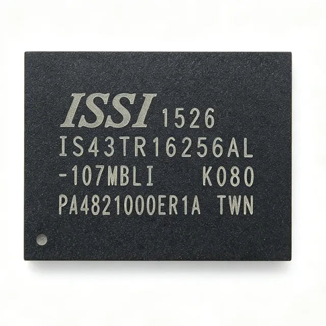
IS43TR16256AL-107MBL - 4Gb DDR3L SDRAM 256Mx16 | ISSI
IS43TR16256AL-107MBL

IS43TR16256AL-107MBL - 4Gb DDR3L SDRAM 256Mx16 | ISSI

The IS43TR16256AL-107MBL is a 4Gb DDR3L SDRAM organized as 256Mx16, operating at 1.35V with a data rate of 1866MT/s. It is housed in a 96-ball TWBGA (9x13mm) package, offering high density and low power consumption for a wide range of computing and embedded applications. DDR3L (Low Voltage DDR3) is a type of synchronous dynamic random-access memory that operates at 1.35V, reducing power consumption by about 15% compared to standard 1.5V DDR3. It is part of the DDR3 SDRAM family, which uses double data rate architecture to transfer data on both edges of the clock, achieving high bandwidth. DDR3L is commonly used in mobile devices, networking equipment, and industrial computing where power efficiency is critical. Key features include a parallel interface with 933 MHz clock speed, 20 ns access time, and support for 1866MT/s data rate. The device supports various burst lengths (8 and 4 with burst chop), on-die termination (ODT), and programmable CAS latency. It operates over a temperature range of 0°C to +95°C (case) and is RoHS compliant. The IS43TR16256AL-107MBL utilizes advanced DRAM process technology, providing high reliability and performance. It features auto-refresh and self-refresh modes, which are essential for low-power standby operation. The 96-ball TWBGA package ensures excellent thermal and electrical performance, making it suitable for space-constrained designs. Typical applications include networking routers and switches, enterprise storage systems, industrial PCs, and embedded computing platforms. Its low voltage and high density make it ideal for memory-intensive applications where power efficiency is a priority. When designing with this device, ensure proper decoupling capacitors are placed near the power pins to minimize noise. The DDR3L interface requires careful PCB layout to maintain signal integrity at high speeds, including matched trace lengths and controlled impedance.

RFQ Kontak
IS43TR16256AL-107MBLI - 4Gb DDR3L SDRAM 256Mx16 | ISSI
IS43TR16256AL-107MBLI

IS43TR16256AL-107MBLI - 4Gb DDR3L SDRAM 256Mx16 | ISSI

The IS43TR16256AL-107MBLI is a 4Gb DDR3L SDRAM organized as 256M x 16 bits, operating at a clock speed of 933 MHz (data rate 1866 Mbps) with a supply voltage of 1.35V. It is housed in a 96-ball TWBGA (9x13mm) package, making it suitable for high-density memory applications in computing, networking, and industrial systems. DDR3L SDRAM (Double Data Rate 3 Low Voltage) is a type of synchronous dynamic random-access memory that operates at a lower voltage (1.35V) compared to standard DDR3 (1.5V), reducing power consumption by up to 20% while maintaining backward compatibility with 1.5V operation. It is part of the DDR3 memory family, which uses double data rate signaling to transfer data on both edges of the clock, achieving high bandwidth for demanding applications. Key features include a 16-bit I/O interface, 4Gbit density, 20ns access time, and support for 1.35V operation with backward compatibility to 1.5V. The device offers high-speed data transfer rates, low power consumption, and is RoHS compliant. The 96-ball TWBGA package provides a compact footprint suitable for space-constrained designs. Technically, the IS43TR16256AL-107MBLI utilizes a 4-bank architecture with 8 internal banks, supporting burst lengths of 8 and 4, and features on-die termination (ODT) for improved signal integrity. It includes programmable CAS latency, additive latency, and write latency, allowing system designers to optimize timing for their specific memory controller. The device also supports auto-refresh and self-refresh modes for power saving. Typical applications include servers, networking equipment, industrial PCs, and embedded systems where high memory density and low power are critical. The 1.35V operation makes it ideal for power-sensitive designs, while the 1866 Mbps data rate supports high-bandwidth workloads. When designing with this device, ensure proper decoupling capacitors near the power pins and follow the layout guidelines in the datasheet to minimize signal integrity issues. The device requires a stable 1.35V supply and careful attention to termination for the address/control and data lines.

RFQ Kontak
IS43TR16256AL-107MBLI-TR - 4Gb DDR3L SDRAM 256Mx16 | ISSI
IS43TR16256AL-107MBLI-TR

IS43TR16256AL-107MBLI-TR - 4Gb DDR3L SDRAM 256Mx16 | ISSI

The IS43TR16256AL-107MBLI-TR is a 4Gb DDR3L SDRAM organized as 256Mx16, operating at 1.35V with a data rate of 1866 Mbps (933 MHz clock). It is housed in a 96-ball TWBGA (9x13mm) package and is designed for low-power applications requiring high memory density. This device is backward compatible with 1.5V DDR3, allowing flexible system design. DDR3L SDRAM is a type of double data rate synchronous dynamic random-access memory that operates at a lower voltage (1.35V) compared to standard DDR3 (1.5V), reducing power consumption by about 20%. It is part of the memory hierarchy in computing systems, serving as main memory for processors, and is widely used in servers, networking equipment, and embedded systems where power efficiency is critical. Key features include a parallel interface with 16-bit data bus, 20ns access time, and support for on-die termination (ODT) and DLL-off mode for power saving. The device supports burst lengths of 8 and 4, and includes programmable CAS latency and additive latency. It operates over a temperature range of 0°C to +95°C (case temperature) for standard operation. The IS43TR16256AL-107MBLI-TR utilizes advanced DRAM process technology to achieve high density and low power. It features auto-refresh and self-refresh modes, with a typical self-refresh current of [DATA_NEEDED: self-refresh current]. The device includes a mode register set (MRS) for configuration, and supports write leveling and read leveling for signal integrity in high-speed systems. Typical applications include servers, networking equipment, industrial computing, and embedded systems where high memory density and low power are required. The 1.35V operation makes it ideal for battery-powered devices and energy-efficient data centers. When designing with this device, ensure proper decoupling capacitors near the power pins and follow the PCB layout guidelines in the datasheet to maintain signal integrity at 1866 Mbps. The device requires a stable 1.35V supply and a separate VDDQ supply for the I/O.

USD $5.60 Kontak
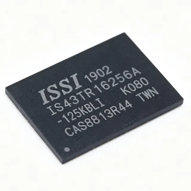
IS43TR16256AL-125KBL - 4Gb DDR3L SDRAM 256Mx16 | ISSI
IS43TR16256AL-125KBL

IS43TR16256AL-125KBL - 4Gb DDR3L SDRAM 256Mx16 | ISSI

The IS43TR16256AL-125KBL is a 4Gbit DDR3L SDRAM organized as 256M x 16, operating from a 1.35V supply with backward compatibility to 1.5V. It is housed in a 96-ball TWBGA (9x13mm) package and supports data rates up to 1600Mbps (800 MHz clock). This memory IC is designed for high-performance computing, networking, and embedded systems requiring low power and high bandwidth. DDR3L (Double Data Rate 3 Low Voltage) is a type of synchronous dynamic random-access memory (SDRAM) that operates at a lower voltage (1.35V) compared to standard DDR3 (1.5V), reducing power consumption by about 20-30% while maintaining similar performance. It is part of the DDR3 family, which uses double data rate signaling to transfer data on both edges of the clock, and is widely used in laptops, servers, and industrial applications where energy efficiency is critical. Key features include a parallel interface with 16-bit data bus, 800 MHz clock frequency, 20 ns access time, and support for 1.35V operation. The device is RoHS compliant and lead-free, making it suitable for environmentally conscious designs. The 96-TWBGA package offers a compact footprint with a 9x13mm body, ideal for space-constrained PCB layouts. Technically, the IS43TR16256AL-125KBL uses a high-density DRAM process, achieving 4Gbit capacity in a single package. It supports standard DDR3L features such as on-die termination (ODT), programmable CAS latency, and burst lengths of 8. The low voltage operation reduces I/O power, while the 20ns access time ensures fast random access for demanding applications. Typical applications include embedded computing, networking equipment (routers, switches), industrial automation, and automotive infotainment systems. Its low power and high density make it ideal for memory-intensive tasks in portable and battery-powered devices. When designing with this component, ensure proper decoupling capacitors near the power pins and follow the layout guidelines in the datasheet to minimize signal integrity issues at high speeds. The 1.35V supply must be regulated accurately to maintain reliable operation.

RFQ Kontak
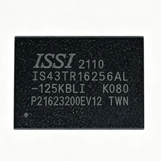
IS43TR16256AL-125KBLI-TR - 4Gbit DDR3L SDRAM 256Mx16 | ISSI
IS43TR16256AL-125KBLI-TR

IS43TR16256AL-125KBLI-TR - 4Gbit DDR3L SDRAM 256Mx16 | ISSI

The IS43TR16256AL-125KBLI-TR is a 4Gbit DDR3L SDRAM organized as 256M x 16, operating at a clock frequency of 800 MHz (data rate 1600 Mbps) with a CAS latency of 11. It is supplied in a 96-ball TWBGA (9x13 mm) package and is designed for low-voltage operation at VDD and VDDQ = 1.35V, with backward compatibility to 1.5V. This memory IC is part of ISSI's DDR3L family, offering high density and bandwidth for a wide range of applications. DDR3L (Double Data Rate 3 Low Voltage) SDRAM is a type of synchronous dynamic random-access memory that transfers data on both edges of the clock signal, effectively doubling the data rate. The 'L' designation indicates low-voltage operation at 1.35V, reducing power consumption by about 20% compared to standard DDR3 at 1.5V. DDR3L is widely used in mobile devices, embedded systems, and industrial computing where power efficiency is critical. It is backward compatible with 1.5V DDR3, allowing flexible system design. Key features include a 4Gbit density, 16-bit data bus, 800 MHz clock speed, and a burst length of 8. The device supports on-die termination (ODT), programmable CAS latency, and auto-refresh and self-refresh modes. It operates over a temperature range of -40°C to +95°C (TC), making it suitable for industrial environments. The 96-ball TWBGA package provides a compact footprint with excellent thermal and electrical performance. Technically, the IS43TR16256AL-125KBLI-TR uses a 1.35V power supply for both core and I/O, reducing power dissipation. It features a 20ns row cycle time (tRC) and a 20ns row active time (tRAS). The device supports a data transfer rate of 1600 Mbps per pin, delivering high bandwidth for memory-intensive applications. The low-voltage operation and industrial temperature range make it ideal for embedded systems that require reliable performance in harsh conditions. Typical applications include industrial automation, networking equipment, embedded computing, and automotive infotainment systems. The 4Gbit density and x16 organization are well-suited for applications requiring moderate memory capacity with a wide data bus. The low-voltage operation helps extend battery life in portable devices and reduces thermal load in dense systems. When designing with this component, ensure proper decoupling capacitors are placed near the power pins to minimize noise. The DDR3L interface requires careful PCB layout to maintain signal integrity at 1600 Mbps. Refer to the ISSI datasheet for detailed timing parameters and layout guidelines.

USD $8.25 Kontak
IS46TR16256A-125KBLA2 - 4Gb DDR3 SDRAM 256Mx16 | ISSI
IS46TR16256A-125KBLA2

IS46TR16256A-125KBLA2 - 4Gb DDR3 SDRAM 256Mx16 | ISSI

The IS46TR16256A-125KBLA2 is a 4Gb DDR3 SDRAM organized as 256Mx16, operating at 1.5V with a data rate of 1600MT/s (800 MHz clock). It is housed in a 96-ball TWBGA (9x13mm) package, offering high-density memory for computing, networking, and industrial applications. This device supports 8 internal banks for concurrent operation and features programmable CAS latency, burst length, and on-die termination (ODT) for signal integrity. DDR3 SDRAM (Double Data Rate Type 3 Synchronous Dynamic Random-Access Memory) is a type of synchronous dynamic random-access memory with a high bandwidth interface, transferring data on both rising and falling edges of the clock. It is the successor to DDR2 and offers higher speeds and lower power consumption, making it a standard choice for main memory in computers, servers, and embedded systems. DDR3 operates at 1.5V, reducing power compared to DDR2's 1.8V, and supports data rates from 800 to 2133 MT/s. Key features include a 20ns tRCD (RAS-to-CAS delay), 290mA operating current, and a temperature range of 0°C to +95°C (Tc). The device is RoHS compliant and supports both standard and low-voltage (1.35V) operation, providing flexibility in power-sensitive designs. The 96-ball TWBGA package with a 9x13mm footprint enables compact PCB layouts, and the 256Mx16 organization simplifies bus design by reducing the number of devices needed for wide data paths. Architecturally, the IS46TR16256A-125KBLA2 uses an 8-bank design with a 16-bit I/O interface, achieving a peak bandwidth of 12.8 GB/s per device. It incorporates DLL (Delay-Locked Loop) for precise clock alignment, and supports programmable read and write latencies. The device also features auto-refresh and self-refresh modes for power management, and on-die termination (ODT) to improve signal quality on high-speed buses. Typical applications include main memory for embedded processors, networking equipment (routers, switches), industrial PCs, and high-performance computing modules. Its high density and speed make it suitable for applications requiring large memory footprints, such as video processing, data acquisition, and telecommunications infrastructure. When designing with this DDR3 device, ensure proper termination and layout for high-speed signals, and follow the JEDEC DDR3 guidelines for power supply decoupling and signal integrity. The device requires a 1.5V supply for VDD and VDDQ, and a separate VREF for address/command signals.

USD $7.20 Kontak
IS61C6416AL-12TLI - 1Mb 64Kx16 12ns Async SRAM | ISSI
IS61C6416AL-12TLI

IS61C6416AL-12TLI - 1Mb 64Kx16 12ns Async SRAM | ISSI

The Integrated Silicon Solution Inc (ISSI) IS61C6416AL-12TLI is a 1 Mbit high-speed asynchronous CMOS Static RAM organized as 65,536 words by 16 bits, with 12 ns access time, housed in a 44-pin TSOP Type II industrial-grade package. It operates from a single 4.5 V to 5.5 V supply and provides a 16-bit parallel I/O bus, making it well suited as cache, buffer, or scratchpad memory in 16-bit and 32-bit embedded systems. What is an asynchronous SRAM? An asynchronous SRAM (Static Random-Access Memory) is a volatile memory device whose read and write cycles are triggered directly by address and control-line transitions, with no external clock required. It sits in the computer-memory hierarchy above DRAM in speed and below on-chip cache in density, and is commonly chosen when deterministic, low-latency random access (single-digit to a few tens of nanoseconds) matters more than density or cost-per-bit. Within ISSI's portfolio it belongs to the IS61C6416AL family of 64Kx16 high-speed CMOS SRAMs. Key features of the IS61C6416AL-12TLI include 12 ns typical access time, low-power CMOS operation with CMOS- and TTL-compatible I/O, automatic power-down when deselected, and separate upper-byte (UB) and lower-byte (LB) enables for byte-wide writes. The 44-pin TSOP-II footprint is JEDEC-standard, simplifying PCB layout and second-sourcing. The industrial temperature grade (-40C to +85C) supports harsh-environment deployment. The device is fabricated using ISSI's high-performance CMOS process, yielding an access time of 12 ns while keeping active and standby currents low. Data is retained as long as power is applied, with no refresh cycles. The active-low write enable (WE#) and chip-enable (CE#) signals give the designer full read/write control, and the byte-control pins (UB#, LB#) allow efficient use of the 16-bit data bus in mixed-width systems. Typical applications include networking line cards, industrial control and instrumentation, automotive infotainment subsystems, telecom routers and switches, RAID controllers, set-top boxes, and any 16-bit or 32-bit embedded CPU system that needs a fast external memory for buffers, FIFOs, or lookup tables. The TSOP-II package and standard JEDEC pinout also make it a popular choice for legacy designs that must be maintained or refreshed. When designing with this part, observe the standard SRAM power-supply decoupling practice: place a 0.1 uF ceramic bypass capacitor as close as possible to the VCC and VSS pins. Unused inputs (UB#, LB#, WE#) should be tied to VCC through a pull-up to prevent unwanted writes. Designers should also note that the asynchronous interface means there is no clock-domain crossing required when interfacing to legacy microcontrollers or DSPs that lack an external memory controller with SRAM timing support. This page synthesizes distributor pricing, parametric drop-in alternatives, and practical design notes that are not gathered in the manufacturer datasheet alone, giving engineers a single source for sourcing, replacement, and PCB-layout decisions.

RFQ Kontak
IS61WV102416DBLL-10TLI - 16Mb Async SRAM 1Mx16 10ns | ISSI
IS61WV102416DBLL-10TLI

IS61WV102416DBLL-10TLI - 16Mb Async SRAM 1Mx16 10ns | ISSI

The ISSI IS61WV102416DBLL-10TLI is a 16-Mbit high-speed asynchronous CMOS static RAM organized as 1M words by 16 bits, housed in a 48-pin TSOP-I package. According to the ISSI datasheet for the IS61/64WV102416DALL/BLL family, the device operates from a single 2.4V to 3.6V supply (with 3.3V nominal) and provides a 10 ns access time, making it suitable for high-performance memory subsystems where deterministic, low-latency read/write cycles are required without the complexity of a DRAM controller. The 'D' prefix designates the lower-voltage 2.4V-3.6V variant, while the 'BLL' suffix indicates the specific speed grade and package option. Asynchronous static RAM (SRAM) is a volatile memory technology that retains data as long as power is applied, without the refresh cycles required by DRAM. Within the broader memory hierarchy, SRAM sits closest to the processor because of its sub-15 ns access times; it is used for cache, look-up tables, scratch-pad buffers, and FIFO storage in networking, industrial, and embedded systems. Compared with synchronous SRAM (such as QDR or DDR SRAM), asynchronous SRAM uses simple chip-enable, output-enable, and write-enable control signals and is ideal for glue-less processor bus interfaces. The IS61WV102416DBLL-10TLI provides fully static operation (no clock required), TTL-compatible I/O levels, common data-in/data-out bus architecture, and an active-low output enable for bus sharing. Power consumption is minimized through a Chip Enable power-down mode, and the device supports industrial temperature range operation. The CMOS fabrication process delivers high noise immunity and low standby current, both of which are critical for battery-backed or energy-conscious designs. Typical applications include industrial controllers, networking line cards, routers and switches requiring fast look-up tables, automotive telematics (non-safety-critical subsystems), medical instrumentation buffers, RAID controllers, and any embedded CPU/MCU design that needs a large, low-latency external data store beyond the on-chip SRAM budget. The wide word width (x16) is well matched to 16-bit and 32-bit microcontrollers and DSPs. When designing with this device, keep in mind that asynchronous SRAM bandwidth is limited by the controller's ability to issue back-to-back read or write strobes, so the 10 ns access time implies roughly 100 MHz equivalent single-transfer throughput per cycle. Decoupling and signal routing must be handled carefully on long busloads to maximize margin. This page synthesizes distributor pricing, drop-in alternative cross-references, and practical design notes that go beyond the manufacturer datasheet to help engineers evaluate and qualify the part quickly.

RFQ Kontak
IS82C54Z96 - 8MHz CMOS Programmable Interval Timer | Renesas
IS82C54Z96

IS82C54Z96 - 8MHz CMOS Programmable Interval Timer | Renesas

The Renesas IS82C54Z96 is a CMOS Programmable Interval Timer manufactured using an advanced 2 micron CMOS process, supplied in a 28-pin PLCC package. It supports clock input frequencies up to 8 MHz and operates from a 4.5 V to 5.5 V single supply. According to the Renesas 82C54 datasheet, the device integrates three independently programmable and functional 16-bit counters, each capable of binary or BCD counting and of handling clock inputs up to 8 MHz (82C54), 10 MHz (82C54-10), or 12 MHz (82C54-12). A programmable interval timer (PIT) is a counter IC that generates precise time delays, event counting, and frequency-division functions under software control. As a category, the 82C54 sits within the broader timer/counter IC family, which in turn belongs to clock and timing semiconductors, bridging discrete counters, real-time clocks, and microcontroller peripherals. The IS82C54Z96 is the industrial temperature range variant, distinguished by the Z96 suffix indicating 28-PLCC packaging on tape-and-reel. Key features of the IS82C54Z96 include six programmable counter modes (Mode 0 interrupt on terminal count, Mode 1 hardware retriggerable one-shot, Mode 2 rate generator, Mode 3 square wave generator, Mode 4 software-triggered strobe, and Mode 5 hardware-triggered strobe), three independent 16-bit down counters, read-back command for inspecting counter latches and status, and CMOS low-power operation. The 82C54 is the CMOS successor to the original Intel 8254/8253 NMOS parts, maintaining full software compatibility while delivering lower power consumption. Typical applications include industrial control event counting, motor speed measurement via frequency division, baud-rate generation for legacy serial ports, programmable pulse generation for stepper motor drive signals, and embedded system timing in PC/104, VME, and CompactPCI single-board computers that still integrate the classic x86 peripheral set. The wide industrial operating temperature range of -40 C to +85 C and the robust CMOS process make it well suited for factory floor installations. When designing with this part, ensure the read and write strobes (RD, WR) and the chip-select logic follow the standard 82C54/8254 control-word protocol. Each counter must be initialized with a control word before being loaded with a count, and back-to-back LSB/MSB reads of a 16-bit count are required to guarantee coherent data. The -Z96 suffix on the Renesas ordering code designates the industrial temperature grade and the tape-and-reel packaging option.

RFQ Kontak
ISD17120SY - 120sec Voice Record/Playback IC | Nuvoton | SOIC-28
ISD17120SY

ISD17120SY - 120sec Voice Record/Playback IC | Nuvoton | SOIC-28

The Nuvoton ISD17120SY is a single-chip multi-message voice record and playback IC from the ChipCorder ISD1700 family, providing 80 to 240 seconds of audio storage (120 seconds typical) in a 28-pin SOIC package. It operates from a single 2.4 V to 5.5 V supply and supports both pushbutton and SPI control interfaces, enabling flexible user interaction in standalone or microcontroller-driven systems. A voice record/playback IC is a fully integrated solid-state audio recorder that combines non-volatile memory, an analog microphone preamplifier, anti-aliasing filter, automatic gain control (AGC), speaker driver, and a PWM output stage on a single die. It belongs to the ChipCorder family of multi-message ICs within the broader audio IC hierarchy: voice record/playback IC -> audio IC -> interface IC -> mixed-signal semiconductor. The on-chip EEPROM-style storage eliminates external memory components, while the integrated class-D-compatible PWM output can directly drive a piezo speaker or feed an external amplifier. Key features include user-friendly pushbutton mode with seven pre-defined triggers (REC, PLAY, FT, ERASE, VOL, RDY, RESET), an SPI-compatible serial interface for microcontroller control, variable sample rate selection (4, 5.3, 6.4, 8 kHz) that adjusts duration and bandwidth, an onboard microphone preamplifier with AGC, and a 2.4 V to 5.5 V single supply that suits both 3.3 V and 5 V rails. The device supports up to 240 seconds of recording at 4 kHz sample rate, with messages stored as solid-state samples requiring no compression algorithm. The ISD17120SY uses Nuvoton's patented multilevel storage technology on a single die, providing non-volatile storage that retains recordings without power. The architecture eliminates the need for digital compression ICs, ADCs, DACs, or external memory, dramatically simplifying BOM for voice prompts in cost-sensitive embedded designs. Voice playback quality is selectable through the sample-rate pin, trading bandwidth (3.4 kHz max) for duration (up to 240 s). Typical applications include voice prompts in industrial equipment, security alarm panels, medical alert devices, toys and consumer appliances, elevator floor announcements, and automotive aftermarket accessories. Designers select this part when they need 60 to 240 seconds of robust, non-volatile audio in a single 28-pin IC. When designing with this device, place the bypass capacitor (typically 0.1 uF) within 5 mm of the VCC pin and route the SP+/SP- differential outputs as short as possible to minimize EMI from the PWM carrier. Verify speaker impedance matches the output stage's drive capability, typically 8 ohm or higher for piezo transducers. This page synthesizes distributor pricing, same-brand duration variants, drop-in alternatives, and practical design notes not found in the manufacturer datasheet.

RFQ Kontak
ISD17240SYI - 240s Multi-Message Voice Record/Playback IC | Nuvoton
ISD17240SYI

ISD17240SYI - 240s Multi-Message Voice Record/Playback IC | Nuvoton

The Nuvoton ISD17240SYI is a single-chip, multi-message voice record and playback IC providing 160 to 480 seconds of audio storage with 4 kHz/5.3 kHz/6.4 kHz/8 kHz selectable sampling rates, housed in a 28-pin SOIC package rated for industrial temperature operation. A multi-message voice record and playback IC (often abbreviated "voice recorder IC" or "ChipCorder") is a self-contained digital audio subsystem that integrates non-volatile storage, an analog microphone preamplifier with Automatic Gain Control, an anti-aliasing filter, a sigma-delta codec, smoothing output filter, and a Class-D-compatible PWM/speaker driver on a single silicon die. In the broader component taxonomy, the ISD1700 family belongs to the audio processor / audio DSP IC category, which itself sits under interface ICs and signal-chain semiconductors used in embedded systems. Because storage is on-chip (no external SPI/I2C EEPROM required), designers eliminate BOM cost and PCB area. Key features include 2.4 V to 5.5 V single-supply operation, on-chip 160 kΩ microphone bias resistor, pushbutton and SPI control interfaces, selectable sampling rates, and message management that supports up to 8 segments. The device supports both standalone pushbutton operation (no MCU required) and SPI-driven operation for microcontroller-managed playback sequencing. Power-down current is sub-microamp, enabling battery-friendly operation in always-on voice prompt designs. The ISD17240SYI uses Nuvoton's proprietary zero-power-on multilevel storage technology, which stores audio samples directly in on-chip non-volatile cells rather than converting to a compressed digital stream. This eliminates codec delay and provides instant-on playback in less than 25 ms from trigger, with no software audio stack. The architecture trades bit-depth and noise floor for ultra-low quiescent power and BOM simplification. Typical applications include industrial voice prompt modules, elevator floor announcers, security alarm voice warnings, medical device audio prompts, vending machine announcements, and consumer appliance voice feedback. The wide 2.4 V to 5.5 V supply range lets the same part serve 3.3 V MCU rails or 5 V industrial buses. When designing with this device, include a decoupling capacitor of at least 0.1 µF directly across VCC and VSSA pins placed within 5 mm, route the analog ground (VSSA) separately back to the regulator, and ensure speaker traces are short and balanced to minimize click/pop artifacts on playback start. This page synthesizes distributor pricing, pin-compatible Nuvoton alternatives in the ISD1700 family, and practical design notes not consolidated in the manufacturer datasheet alone.

RFQ Kontak
ISD1760SY - 60s Voice Record/Playback IC 2.4-5.5V | Nuvoton
ISD1760SY

ISD1760SY - 60s Voice Record/Playback IC 2.4-5.5V | Nuvoton

The Nuvoton ISD1760SY is a single-chip multi-message voice record and playback IC providing up to 60 seconds of audio storage in a 28-pin SOIC (300 mil) package, operating from a 2.4 V to 5.5 V single supply. It integrates an on-chip oscillator, anti-aliasing filter, smoothing filter, automatic gain control, microphone preamplifier, and speaker driver, eliminating most external components for voice-capture applications. What is a voice record/playback IC? A voice record/playback IC is a single-chip audio subsystem that captures analog microphone input, digitizes and stores the audio in on-chip non-volatile memory, and reconstructs the analog waveform on demand. It sits hierarchically under interface ICs -> audio ICs -> signal chain semiconductors, and is distinct from MP3/WAV codec ICs because storage is performed entirely on-chip using Nuvoton's patented multilevel storage (MLS) technology. Key features of the ISD1760SY include user-selectable 4 kHz, 6.4 kHz, 8 kHz, and 12 kHz sampling rates that trade recording duration for audio bandwidth, a 120-second maximum duration at the lowest sample rate (mode dependent), built-in push-button interface with debounce logic, an SPI-compatible control port for MCU-driven playback, and integrated class-D-compatible PWM output capable of driving a small speaker directly through an external transistor or buffer. Standby current is below 1 uA, making it well suited to battery-powered products. The device uses Nuvoton's zero-power-message storage scheme that retains recorded audio without any supply current and supports random-address message playback for systems that require multiple prompts. The internal architecture combines a switched-capacitor anti-alias filter ahead of the storage array and a smoothing filter on playback, removing the need for external op-amps in most designs. Typical applications include voice-prompt industrial control panels, elevator floor announcers, security alarm annunciators, talking toys, medical device audio feedback, and consumer appliance voice prompts. Designers select the ISD1760SY when they need a self-contained voice subsystem without DSP overhead or external Flash storage. When designing in this part, observe the 2.4 V minimum supply and ensure the speaker driver transistor is sized for the expected load. The push-button interface supports up to six direct-trigger inputs, reducing GPIO demand on the host MCU and simplifying front-panel wiring in stand-alone playback designs. This page synthesizes XAIPART distributor pricing, drop-in same-brand alternatives from the Nuvoton ISD1700 family, and practical design notes that are not consolidated on a single manufacturer datasheet page.

RFQ Kontak
ISL26104AVZ - 24-Bit 4kSPS 4-Ch Sigma-Delta ADC | Renesas
ISL26104AVZ

ISL26104AVZ - 24-Bit 4kSPS 4-Ch Sigma-Delta ADC | Renesas

The Renesas ISL26104AVZ is a 24-bit low-noise delta-sigma analog-to-digital converter with four differential multiplexed input channels, an integrated low-noise programmable-gain amplifier (PGA), and an output data rate up to 4 kSPS, housed in a 28-pin TSSOP package. Its headline parameters are 24-bit resolution, 4 fully differential input channels, and a programmable output word rate from 2.5 SPS to 4 kSPS, all integrated in a single analog front-end IC. A delta-sigma (sigma-delta) ADC is a type of oversampling converter that uses a high-frequency modulator and digital decimation filtering to achieve very high resolution at the cost of absolute input bandwidth. In the broader taxonomy, the ISL26104 belongs to the precision ADC product family, which sits within data converters, a sub-category of mixed-signal integrated circuits. Delta-sigma ADCs are widely used in industrial weighing, process control, temperature measurement, and strain-gauge instrumentation because they trade conversion speed for excellent noise performance and integral linearity. Key features of the ISL26104AVZ include the on-chip low-noise PGA with gains from 1x to 128x, which allows direct connection of low-amplitude signals such as load cells, thermocouples, and bridge sensors without an external instrumentation amplifier. The device supports an external differential reference and offers a serial SPI-compatible output interface. Its integrated digital filter delivers 50 Hz and 60 Hz mains-rejection at appropriate output data rates, simplifying design for industrial environments with significant line-frequency noise. The device operates from a single analog supply (typically +5 V) and a digital supply, with an internal clock. The 28-pin TSSOP package provides a small footprint while still allowing hand-soldering for prototypes and small production runs. According to the Renesas datasheet, the ISL26104 also shares pin-out compatibility with the 2-channel ISL26102, giving designers a simple upgrade path when more channels are required. Typical applications include industrial weighing scales, load-cell signal conditioning, multi-channel temperature acquisition, pressure transducers, and precision weigh-in-motion modules. The combination of an integrated PGA and high-resolution conversion removes most of the analog signal-chain complexity for sensor readout. Designers should note that the PGA gain, output data rate, and digital-filter bandwidth trade off against each other: higher PGA gain reduces input-referred noise but narrows the usable bandwidth, while lower output data rates improve noise-free resolution at the expense of conversion speed.

RFQ Kontak
ISL26104AVZ-T7A - 24-bit 4kSPS 4-Ch Sigma-Delta ADC | Renesas
ISL26104AVZ-T7A

ISL26104AVZ-T7A - 24-bit 4kSPS 4-Ch Sigma-Delta ADC | Renesas

The Renesas ISL26104AVZ-T7A is a 24-bit low-noise 4-channel delta-sigma analog-to-digital converter with on-chip programmable-gain amplifier and 4 kSPS maximum output data rate, housed in a 28-pin TSSOP package. It accepts four differential multiplexed inputs and operates from an analog supply of 4.75 V to 5.25 V and a digital supply of 2.7 V to 5.25 V. The serial interface provides SPI/QSPI/MICROWIRE-compatible read/write access to on-chip registers for channel selection, gain (1x-128x), and output data rate (2.5 SPS to 4 kSPS). A delta-sigma ADC is a type of oversampling converter that trades speed for resolution: an internal modulator shapes quantization noise away from the band of interest, and a digital decimation filter removes that noise to extract a high-resolution 24-bit code. The ISL26104's exceptionally low input-referred noise (about 10 nV/√Hz PGA equivalent, per the Renesas datasheet) places it firmly in the precision instrumentation category used in weigh scales, bridge transducers, and thermocouple acquisition. Key features include 24-bit noise-free resolution at lower data rates, a PGA with gains of 1, 2, 4, 8, 16, 32, 64, and 128, a single-cycle settling digital filter, an integrated low-drift reference input, and a low quiescent current ideal for loop-powered or battery instruments. The four differential input channels are sequentially scanned via the MUX register, simplifying multi-sensor front ends by removing external analog switches. Typical applications include industrial load-cell weigh scales, RTD and thermocouple temperature acquisition, pressure-sensor signal conditioning, multi-zone gas detection front ends, and precision laboratory instrumentation where 4 kSPS covers typical slow-control loops without sacrificing effective resolution. When designing with this part, place 0.1 uF decoupling capacitors within 5 mm of AVDD and DVDD, keep the analog and digital grounds separated and joined only at the exposed pad, and choose an RGEF/A external reference or pair of input resistors to set the common-mode for thermocouple measurement. This page synthesizes distributor stock and pricing as of 2026-10-13, drop-in TSSOP-28 alternatives from the same and cross-brand product families, and practical design notes not found in the manufacturer datasheet.

RFQ Kontak
ISL26134AVZ-T7A - 24-bit Low-Noise Delta-Sigma ADC | Renesas
ISL26134AVZ-T7A

ISL26134AVZ-T7A - 24-bit Low-Noise Delta-Sigma ADC | Renesas

The Renesas ISL26134AVZ-T7A is a 24-bit, low-noise, 4-input, 1-channel sigma-delta analog-to-digital converter housed in a 28-pin TSSOP surface-mount package. It integrates a very low-noise programmable-gain amplifier (PGA) front end with up to 128x gain, an internal 2.5V reference, and on-chip calibration registers, all on a single mixed-signal IC designed for high-resolution measurement. A delta-sigma ADC is a type of analog-to-digital converter that uses oversampling and noise shaping to achieve very high resolution at the expense of input bandwidth. The ISL26134 sits at the top of the ADC hierarchy (delta-sigma -> ADC -> data converter -> data acquisition IC -> signal chain), enabling 24-bit effective resolution for DC and low-frequency measurements such as load-cell, strain-gauge, and temperature bridge readouts. Key features include 4 differential or 7 single-ended input channels selectable through a digital multiplexer, a true 24-bit no-missing-codes output, integrated PGA gain from 1x to 128x, an auxiliary 24-bit DAC for sensor excitation, and a simple SPI-compatible serial interface. RMS noise below 8 nV at low sample rates and a calibrated integral nonlinearity of better than 0.0015% of full scale make it suitable for precision weighing scales and laboratory instrumentation. The architecture combines a chopper-stabilized front end, a third-order modulator, and a digital SINC1/SINC3 FIR decimation filter. The chopper stage removes 1/f flicker noise; the modulator pushes quantization noise well above the baseband where the SINC filter removes it. Internal gain and offset calibration registers compensate for drift over temperature. Typical applications include industrial weigh scales, temperature/pressure bridge transmitters, multichannel data loggers, and 6-digit digital multimeter front ends. The wide PGA range lets the same IC read directly from low-output sensors such as load cells without external instrumentation amplifiers. Designers should keep analog and digital ground planes separated and place the bypass capacitors within 3 mm of the supply pins to avoid digital switching noise coupling into the modulator. For maximum SNR, choose the lowest output data rate that still meets the application bandwidth, since each halving of data rate reduces input-referred noise by approximately 30%.

RFQ Kontak
ISL26310FBZ - 12-bit 125kSPS SAR ADC | Renesas
ISL26310FBZ

ISL26310FBZ - 12-bit 125kSPS SAR ADC | Renesas

The Renesas ISL26310FBZ is a 12-bit, 125 kSPS successive-approximation-register (SAR) analog-to-digital converter with single-ended and differential inputs, housed in an 8-pin SOIC (NB) package. It features low power consumption, single +5V analog supply operation, and an SPI/QSPI/MICROWIRE-compatible serial interface, making it a fit for embedded industrial and instrumentation digitizer front ends. A SAR ADC is a successive-approximation-register analog-to-digital converter. It uses a binary search algorithm and an internal precision DAC to compare the sampled input against a reference voltage, producing a digital code in N conversion cycles for an N-bit result. SAR ADCs excel at low-latency, single-shot conversions with no pipeline delay, occupy a small footprint, and draw no idle current between conversions - ideal for multiplexed channel scanning, low-duty-cycle battery-powered sensing, and microcontroller-interfaced data acquisition where simplicity and deterministic latency matter more than maximum throughput. Key specifications of the ISL26310FBZ include 12-bit resolution, 125 kSPS maximum sampling rate, single +5V analog supply with +3.3V/+5V digital supply, single-ended and true-differential input pair operation, integrated track/hold, and a low-power serial interface that supports SPI, QSPI, and MICROWIRE protocols. The device includes a hardware shutdown pin to reduce current draw between conversions. The ISL26310FBZ is part of the ISL26310/11/12/13/14/15/19 pin-compatible family that scales channel count, input configuration (single vs. differential), and resolution up to 14-bit. This lets designers migrate between channel counts without PCB redesign. The internal SAR core uses a charge-redistribution DAC array with auto-calibrated capacitor matching to deliver linearity performance consistent across the full industrial temperature range. Typical applications include industrial process control loop monitoring, portable battery-powered instrumentation, multichannel data acquisition front ends, isolated sensor signal conditioning, and remote telemetry / SCADA modules. The 125 kSPS rate supports per-channel rates up to 10 kSPS in multiplexed multi-channel systems, sufficient for vibration, strain, and temperature acquisition. When using this device, decouple AVDD and DVDD separately close to the pins with 10uF bulk plus 0.1uF ceramic bypass, and add a 0.1uF cap on REF+ to ground. The shutdown pin (SHDN) can be tied to logic high for always-on operation; drive low between conversions to minimize system power. This page synthesizes current distributor pricing, drop-in pin-compatible alternatives from the ISL2631x family, and practical design notes not collated in the manufacturer datasheet.

RFQ Kontak
ISL26310FBZ-T - 12-bit 125kSPS SAR ADC Single-Channel | Renesas
ISL26310FBZ-T

ISL26310FBZ-T - 12-bit 125kSPS SAR ADC Single-Channel | Renesas

The Renesas ISL26310FBZ-T is a 12-bit, 125 kSPS successive-approximation-register (SAR) analog-to-digital converter with a single differential input channel, supplied in an 8-pin SOIC package and qualified for industrial temperature operation. It accepts single-ended or differential analog inputs, communicates over an SPI/serial interface, and operates from a 2.7 V to 5.5 V analog supply with low power dissipation suitable for battery-powered and always-on measurement systems. A SAR ADC is a type of analog-to-digital converter that performs a binary search through an internal capacitive DAC to digitize an analog input, completing a conversion in a fixed number of clock cycles. Within the data-acquisition hierarchy, the ISL26310FBZ-T sits between general-purpose 8-/10-bit ADCs and higher-resolution 14-/16-/24-bit delta-sigma converters, offering a balanced trade-off of speed, resolution, and power. Renesas's proprietary input multiplexer and input buffer amplifier reduce external drive requirements, simplifying front-end design. Key features include 12-bit resolution with no missing codes, a 125 kSPS maximum sampling rate, an internal 2.5 V reference, and integrated input buffer that reduces kickback and drive demands. The single-channel differential input accepts bipolar input ranges when properly biased, and the SPI-compatible serial interface supports daisy-chaining of multiple converters to minimize MCU pin count. Architecture highlights include a low-noise charge-redistribution SAR core, an automatic input multiplexer, and an on-chip oscillator. The 8-pin SOIC package has a thermal resistance of approximately 110 C/W and a small footprint (3.90 mm body width), enabling compact PCB layouts for portable instruments and process-control modules. Typical applications include portable instrumentation, process-control analog input modules, battery-powered sensor conditioning loops, and industrial data-acquisition front ends. The wide 2.7 V to 5.5 V supply range and low power consumption make the part well suited to distributed I/O nodes where heat and energy budget matter. When designing with this device, add anti-alias filtering on the analog input prior to the ADC and ensure the SPI SCLK stays within the converter's rated timing budget. Decoupling the AVDD pin with 100 nF and 10 uF capacitors placed close to the package pins is recommended to keep digital switching noise out of the conversion result. This page synthesizes verified distributor pricing, drop-in same-brand and cross-brand alternatives, and practical design notes that go beyond the datasheet's typical-application drawings, giving engineers a single reference for sourcing and second-sourcing decisions.

RFQ Kontak
ISL26310FBZ-T7A - 12-bit 125kSPS SAR ADC, 1-Ch, 8-SOIC | Renesas
ISL26310FBZ-T7A

ISL26310FBZ-T7A - 12-bit 125kSPS SAR ADC, 1-Ch, 8-SOIC | Renesas

The Renesas ISL26310FBZ-T7A is a 12-bit resolution successive-approximation-register (SAR) analog-to-digital converter that samples at 125 kSPS in an 8-pin SOIC package. The single-channel device supports single-ended inputs with bipolar analog input ranges up to ±10 V (or 0 V to 12 V unipolar) when paired with ±5 V or +5 V external supplies. Its SPI-/QSPI-/MICROWIRE-compatible serial interface simplifies connection to microcontrollers, DSPs, and FPGAs in data-acquisition designs. The ISL26310FBZ-T7A is a member of the ISL2631x SAR ADC family which includes 1/2/4/8-channel single-ended and 1/2/4-channel differential input options. An SAR ADC is a sampling converter that uses a binary-searched capacitor DAC against the input voltage, producing an inherently low-latency digital conversion. It belongs to the broader signal-chain family: ADC -> data converter -> analog front-end -> data acquisition IC -> signal-chain component -> semiconductor. The bipolar-CMOS process gives the part low power consumption while preserving high DC accuracy and excellent linearity over temperature. Key features include 12-bit no-missing-codes performance, ±1 LSB INL/DNL typical, a low 5 mW power dissipation at 125 kSPS with 5 V supplies, and hardware/software shutdown that drops quiescent current to a few hundred nanoamperes. An internal input multiplexer (on multi-channel variants) plus a combination buffer amplifier reduces the need for external signal-conditioning, lowering the analog front-end bill of materials in instrumentation and process-control boards. Typical applications are industrial process control loops, multi-channel PLC analog input modules, portable/battery-powered instrumentation, and data-acquisition (DAQ) front ends that require ±10 V input ranges, ±5 V dual supplies, and a small serial-only footprint. Two of those industries, factory automation and mobile instrumentation, depend heavily on the part's robustness over temperature. When designing with this device, choose an external reference and op-amp front end sized to the source impedance to keep conversion error below 1 LSB at the full 125 kSPS data rate.

RFQ Kontak
ISL26311FBZ - 12-bit 125kSPS SAR ADC | Renesas Electronics
ISL26311FBZ

ISL26311FBZ - 12-bit 125kSPS SAR ADC | Renesas Electronics

The Renesas Electronics (formerly Intersil) ISL26311FBZ is a 12-bit, 125 kSPS successive-approximation (SAR) analog-to-digital converter in an 8-pin SOIC package with one differential/single-ended input channel. It delivers low power consumption, supports single-ended and differential input modes, and integrates multiple input channels for flexible signal-chain design in industrial, instrumentation, and process-control applications. An SAR (Successive Approximation Register) ADC is a type of analog-to-digital converter that uses a binary search algorithm with an internal DAC and comparator to digitize an analog input one bit at a time per clock cycle. SAR ADCs sit in the broader hierarchy of ADC architectures (SAR -> Nyquist-rate ADC -> data converter -> mixed-signal IC -> semiconductor) and are favored for medium-resolution, medium-speed acquisitions where low latency, deterministic sampling, and excellent DC accuracy are required. Key features include 12-bit resolution, 125 kSPS maximum sampling rate, single-channel input with single-ended or differential operation, an internal reference, and a SPI/QSPI/MICROWIRE-compatible serial interface. The wide analog input range and integrated input multiplexer simplify front-end signal conditioning, while the small 8-pin SOIC footprint supports compact PCB layouts in space-constrained designs. The device uses a low-noise charge-redistribution SAR architecture with an input track-and-hold, achieving ±1 LSB INL and low aperture jitter. The robust digital interface simplifies host-MCU integration, and the part operates from a single analog supply, reducing external component count. Its low power consumption makes it suitable for battery-powered data-acquisition systems. Typical applications include industrial process control loop monitoring, portable instrumentation and data loggers, multi-channel sensor signal acquisition, medical patient-monitoring front ends, and precision measurement equipment. The single-supply operation simplifies isolated sensor interface designs where low power and small package size are critical. When designing with this ADC, ensure the analog input does not exceed the supply rails and use the recommended bypass capacitors on AVDD and DVDD. The internal reference may be bypassed with an external capacitor for low-noise operation; verify timing against the SAR acquisition window in your specific signal-chain design. This page synthesizes distributor pricing, drop-in alternatives, and practical design notes not found in the manufacturer datasheet, providing engineers a single reference for sourcing and substituting the ISL26311FBZ.

RFQ Kontak
ISL26311FBZ-T7A - 12-bit 125kSPS SAR ADC, 1-Ch Diff | Renesas
ISL26311FBZ-T7A

ISL26311FBZ-T7A - 12-bit 125kSPS SAR ADC, 1-Ch Diff | Renesas

The Renesas ISL26311FBZ-T7A is a 12-bit, 125 kSPS successive-approximation-register (SAR) analog-to-digital converter with a single differential input channel, housed in an 8-pin SOIC-N package and supplied on a 7-inch tape and reel. According to the manufacturer datasheet, the device operates from a single 2.7 V to 5.25 V analog supply and provides a high-speed SPI-/serial-compatible digital interface, integrating the sample-and-hold, reference input, and conversion clock on-chip to minimize external BOM. A SAR ADC is a type of data converter that uses a binary-search successive-approximation algorithm to digitize an analog input, trading resolution for speed. SAR converters sit within the broader ADC family (alongside delta-sigma, pipeline, and flash ADCs) and are widely preferred in multiplexed data-acquisition systems, industrial control loops, and portable instrumentation where deterministic latency, low power, and small package size are required. The ISL26311 belongs to the ISL26310/11/12/13/14/15/19 pin-compatible SAR ADC family from Renesas, which lets designers reuse one PCB footprint across multiple channel-count variants. Key features of the ISL26311FBZ-T7A include 12-bit resolution (no missing codes), true differential analog inputs for high common-mode rejection, integrated low-drift reference buffer support, and a 1-/8-pin SOIC footprint that simplifies layout in space-constrained designs. The low-power architecture targets 125 kSPS throughput at sub-mW conversion rates while preserving excellent AC and DC linearity for precision sensor read-back. The single-channel input simplifies firmware and routing when only one precision voltage must be measured. Typical applications for the ISL26311FBZ-T7A include industrial process control, isolated sensor front-ends, multichannel data-acquisition systems where it is paired with multiplexers, battery management monitoring, and portable medical instrumentation. The differential input allows direct connection to bridge sensors such as load cells and strain gauges without an external instrumentation amplifier, reducing board area and cost. When designing with this ADC, ensure the analog supply is well decoupled with a 10 uF bulk plus 0.1 uF ceramic placed as close as possible to the AVDD pin. Reference decoupling on the REF pin is critical to achieving rated noise performance. The digital lines should be kept short and routed away from the analog input to minimize coupling. This page synthesizes distributor pricing, the ISL2631x pin-compatible family, and practical design notes that are not collated in the manufacturer datasheet.

RFQ Kontak
ISL26312FVZ - 12-bit 125kSPS 2-ch Diff SAR ADC | Renesas
ISL26312FVZ

ISL26312FVZ - 12-bit 125kSPS 2-ch Diff SAR ADC | Renesas

The Renesas ISL26312FVZ is a 12-bit, 125 kSPS, dual-channel differential-input successive-approximation-register (SAR) analog-to-digital converter housed in a 16-pin TSSOP package. It operates from a single 2.7 V to 5.25 V analog supply with a separate digital I/O supply (1.8 V to AVDD), supports single-ended or true differential inputs, and provides an SPI-compatible serial interface with daisy-chain capability. The part is pin-compatible with the wider ISL26310/11/13/14/15/19 family, allowing channel-count scaling without board rework. A SAR ADC is a successive-approximation-register analog-to-digital converter that uses a binary-search algorithm and a precision internal DAC to converge on the input voltage in one conversion cycle per bit. SAR ADCs sit in the broader category hierarchy of data converter -> ADC -> successive-approximation ADC -> precision data acquisition IC, and are typically chosen over delta-sigma converters when low latency (no pipeline delay), wide input bandwidth, and true-differential inputs are required in industrial control and instrumentation front ends. Key features include excellent linearity over supply and temperature, an input multiplexer combined with a low-drive buffer amplifier that relaxes external driver requirements, and a proprietary input MUX that supports 1-, 2-, 4-, and 8-channel single-ended configurations as well as 1-, 2-, and 4-channel differential configurations across the family. Typical INL/DNL is better than 1 LSB and the device draws only a few mW at full throughput, making it suitable for battery-powered monitoring. Typical applications include industrial process control loop measurement, multi-channel sensor data acquisition (temperature, pressure, strain gauges), battery monitoring and management systems, motor-control feedback, and instrumentation front-ends that require low-latency differential conversion. Designers appreciate the combination of small TSSOP footprint, simple SPI interface, and high DC accuracy. When designing with this device, place the analog and digital ground planes with proper partitioning and keep the REFIN decoupling capacitor as close to the pin as possible to maintain DC accuracy. Use a low-impedance input buffer when driving the AIN pins from high-impedance sensors. This page synthesizes distributor pricing, drop-in pin-compatible alternatives within the ISL2631x family, and practical design notes that complement the manufacturer datasheet for fast design-in decisions.

RFQ Kontak
ISL26312FVZ-T - 12-bit 125kSPS SAR ADC, 2-ch Diff | Renesas
ISL26312FVZ-T

ISL26312FVZ-T - 12-bit 125kSPS SAR ADC, 2-ch Diff | Renesas

The Renesas ISL26312FVZ-T is a 12-bit, 125 kSPS successive-approximation register (SAR) analog-to-digital converter with two differential input channels, offered in a 16-pin TSSOP package for industrial and instrumentation front-ends. As a member of the ISL26310/11/12/13/14/15/19 family, it provides excellent linearity across supply and temperature variations while consuming only 11 mW at full throughput and dropping to a typical 8 µA between conversions when auto power-down is enabled, making it well suited for battery-aware data-acquisition systems. A SAR ADC is a converter architecture that performs a binary search through an internal capacitive charge-redistribution DAC, evaluating one bit per conversion clock and producing the result on a single clock cycle without requiring a pipeline delay. SAR ADCs are prized for low-latency triggering, deterministic behavior on multiplexed inputs, and excellent DC linearity with no missing codes - and they remain the dominant choice for multi-channel precision industrial front-ends where both sample-accurate acquisition and lowest idle power matter. Key specifications of this part include 12-bit resolution, 125 kSPS maximum sampling rate, ±10 V input range when configured for bipolar operation, true-differential analog inputs, an SPI-compatible serial interface, single 2.7 V to 5.25 V supply operation, and automotive-grade -40 °C to +125 °C temperature support. The 0.7 LSB typical DNL, on-chip track-and-hold, and integrated input multiplexer enable direct sensor interfacing with minimal external signal conditioning. The on-chip sequencer and auto power-down state machine, combined with a flexible analog input mux, make the ISL26312FVZ-T straightforward to drop into multiplexed sensor panels, isolated transducer front-ends, and process-control loops. The SPI port operates in mode 0 and mode 3 and is easily framed by most FPGAs, microcontrollers, and digital isolators, so a single part can serve both 3.3 V MCU rails and 5 V legacy PLC backplanes. Typical uses include industrial process instrumentation, multi-channel data loggers, motor-control feedback, isolated sensor readouts, and precision weigh-scale / strain-gauge signal chains. The wide 2.7 V to 5.25 V supply range tolerates either a regulated 3.3 V rail or a 5 V USB- or PLC-derived supply. Across all of these uses, the TSSOP-16 footprint keeps the converter area cost low and routing simple. When designing with this device, place a 100 nF decoupling capacitor within 5 mm of the AVDD pin and a 10 µF bulk capacitor on the analog supply, route the analog and digital grounds through a star tie at the AGND pin, and verify SPI mode (CPOL/CPHA) against the host controller. For low-distortion input buffers, an op-amp rail-to-output driver such as the OPA2188 is recommended to avoid degrading the converter's DNL. This page combines distributor pricing, pin-compatible drop-in alternatives, and application design notes into a single reference - saving engineering time versus cross-checking three separate component databases.

RFQ Kontak
ISL26312FVZ-T7A - 12-bit 125kSPS Dual-Channel SAR ADC | Renesas
ISL26312FVZ-T7A

ISL26312FVZ-T7A - 12-bit 125kSPS Dual-Channel SAR ADC | Renesas

The Renesas ISL26312FVZ-T7A is a 12-bit, 125 kSPS low-power successive-approximation-register (SAR) analog-to-digital converter (ADC) with two differential input channels, packaged in a 16-pin TSSOP and shipped on a 7-inch tape-and-reel carrier. A SAR ADC is a type of data converter that compares the sampled input voltage against a precision DAC one bit at a time over successive clock cycles, achieving deterministic latency and excellent DC accuracy at moderate sampling rates. SAR converters sit in the broader hierarchy: data converter -> ADC -> SAR ADC -> precision acquisition IC -> mixed-signal semiconductor. They are preferred over delta-sigma or pipeline ADCs whenever multiplexed multi-channel inputs, low power, simple SPI/QSPI/MICROWIRE digital interfaces, and excellent AC performance are needed in industrial instrumentation. Key features of the ISL26312FVZ-T7A include 12-bit resolution, 125 kSPS throughput, two differential input channels (selectable from up to four single-ended or two differential inputs through an internal analog multiplexer), an SPI/QSPI/MICROWIRE-compatible serial interface, and a wide 2.7 V to 5.25 V analog supply range that supports single-supply 3.3 V or 5 V rails. Technical depth comes from the proprietary input multiplexer with an integrated input buffer amplifier, which reduces input drive requirements and minimizes channel-to-channel crosstalk. The device draws microamp-level supply current at lower sample rates, and offers a hardware power-down pin for battery-sensitive applications. Linearity is maintained across the industrial -40 C to +125 C temperature range, supported by a built-in track/hold and a robust internal reference option. Typical applications include industrial process control loops, multi-channel data-acquisition front-ends, isolated sensor signal chains, PLC analog input modules, and battery-powered instrument clusters where the combination of low power draw and clean 12-bit DC performance yields high measurement integrity. When designing with this part, place a 10 nF ceramic decoupling capacitor directly at the AVDD pin and a 1 uF bypass at DVDD to keep the SAR comparator noise floor low. The REFIN/REFOUT pin accepts either an external reference or uses the internal 2.5 V reference - drive REFOUT with a low-ESR 10 uF ceramic for best AC performance. This page synthesizes distributor pricing, drop-in alternatives within the ISL26310/11/12/13/14/15/19 family, and practical design notes not collected in the manufacturer datasheet alone.

RFQ Kontak
ISL26314FVZ - 12-bit 125kSPS 4-CH Differential SAR ADC | Renesas
ISL26314FVZ

ISL26314FVZ - 12-bit 125kSPS 4-CH Differential SAR ADC | Renesas

The Renesas ISL26314FVZ is a 12-bit, 125 kSPS successive-approximation-register (SAR) analog-to-digital converter with 4 differential input channels, packaged in a 16-pin TSSOP. It operates from a single 2.7 V to 5.25 V analog supply and a 1.8 V to 3.6 V digital supply, drawing only 6.4 mW at full speed, which makes it well-suited to low-power multi-channel data-acquisition front-ends. What is a SAR ADC? A successive-approximation-register analog-to-digital converter is a sampling ADC architecture that performs one bit-trial per clock cycle using a binary search across an internal capacitive DAC. SAR ADCs are valued for deterministic latency (one conversion = N clock cycles), zero pipeline delay, excellent DC linearity, and low power consumption - they sit in the IC hierarchy: ADC -> data converter -> mixed-signal IC -> semiconductor. SAR converters are preferred over delta-sigma converters for multiplexed multi-channel sampling where per-channel latency must be deterministic, and over pipeline ADCs when power and simplicity matter more than very high sample rates. Key features include 4 differential inputs (expandable to 8 single-ended via software), 125 kSPS maximum throughput, ±1 LSB INL (typical), a proprietary input multiplexer with integrated buffer amplifier that reduces external drive requirements, and a wide operating temperature range of -40°C to +125°C. The device also integrates an internal 2.5 V reference (10 ppm/°C typical), an SPI/QSPI/MICROWIRE-compatible serial interface, and a hardware / software shutdown pin that reduces supply current to under 1 µA between conversions. The ISL26314 is implemented on a low-power CMOS process. An internal charge redistribution DAC combined with the proprietary input multiplexer allows direct connection of high-impedance sensors without external instrumentation amplifiers, simplifying the analog front end. The part is part of a broader pin-compatible family (ISL26310/11/12/13/14/15/19) offering 1, 2, 4, and 8 single-ended and 1, 2, 4 differential channel counts - enabling one PCB layout to scale across product variants. Typical applications include industrial process control, 4-20 mA loop digitization, multi-cell battery monitoring, programmable logic controller (PLC) analog input modules, weigh scales, and temperature measurement front-ends (RTD/thermocouple with external amplifier). When designing with this part, note that the input buffer lowers kick-back current into high-source-impedance sensors, but adding an RC anti-alias filter ahead of the input requires careful selection to avoid degrading settling at 125 kSPS. Use the SHDN pin to drop idle channels to microamp-level quiescent current in battery-powered multi-channel systems. This page synthesizes distributor pricing, same-family pin-compatible drop-in alternatives, and design notes not found in the manufacturer datasheet alone.

RFQ Kontak