Mga Interface IC
Subkategorya
Mga Produkto (3,100+)

SP490ECN/TR - 5Mbps RS-485/RS-422 Transceiver | MaxLinear
The MaxLinear SP490ECN/TR is a 5 Mbps RS-485/RS-422 differential line transceiver with one driver and one receiver, operating from a single 5 V supply in an 8-pin SOIC package. The device combines a differential bus driver and differential receiver with ±200 mV receiver input sensitivity and supports balanced differential signaling over extended cable distances. Its BiCMOS implementation provides low power consumption for industrial communications equipment. An RS-485/RS-422 interface transceiver is a semiconductor product category used to convert logic-level signals into balanced differential transmissions and to recover differential signals from noisy buses. Within the broader hierarchy, the SP490ECN/TR is an interface transceiver, a bus-line transceiver, and a communications interface IC designed for industrial data links. Balanced signaling improves noise immunity by representing each signal as a difference between two conductors rather than as a single-ended voltage. The SP490ECN/TR supports data rates up to 5 Mbps while maintaining the operating characteristics required by RS-422 and RS-485 networks. Its single 5 V supply simplifies interface design, and the ±200 mV receiver sensitivity permits operation with attenuated or electrically noisy differential signals. The one-driver, one-receiver arrangement supports full-duplex point-to-point RS-422 links and multidrop RS-485 applications. The manufacturer datasheet also identifies compatibility with LTC490 and SN75179 devices. The transceiver combines a low-power BiCMOS driver and receiver with differential bus connections. Its receiver converts the difference between the positive and negative bus inputs into a single-ended logic output, while the driver converts a differential logic input into a complementary bus output. The wide receiver common-mode range is specifically identified in the manufacturer datasheet, helping the device tolerate voltage offsets imposed by grounds, cable terminations, and installed equipment on an industrial bus. Typical applications include industrial factory automation, point-to-point telemetry links, building-control networks, RS-422 equipment interfaces, and RS-485 multidrop communications. The 5 Mbps maximum signaling rate supports moderate- and high-speed data transfer, while the 8-pin SOIC format supports compact, surface-mounted assemblies. The same electrical interface can also serve industrial sensors, remote I/O modules, data acquisition equipment, and communication links between controllers and peripheral equipment. Designers should preserve the transceiver's differential signal routing and provide correct bus biasing and termination. Power-supply decoupling should be placed close to the device, while the driver and receiver ground connection should remain compatible with the interface reference plane. Termination is required according to the selected RS-422 or RS-485 topology rather than being applied indiscriminately to every node. Cable length, node spacing, grounding, and common-mode limits must be evaluated together for reliable operation. This product page combines the verified MaxLinear datasheet, distributor availability, pricing evidence, pin information, and package details with practical interface-design guidance. It also distinguishes the SP490ECN/TR from related SP490E and SP490ECN-L/TR variants by data rate while identifying only same-package drop-in alternatives supported by the supplied manufacturer and cross-reference information.

SP490ECP-L - 10Mbps Full-Duplex RS-485 IC | MaxLinear
The MaxLinear, Inc. SP490ECP-L is a 10 Mbps full-duplex RS-485/RS-422 differential line transceiver packaged in an 8-pin PDIP package. It combines one differential driver and one differential receiver, supports +5 V-only operation, and is intended for bidirectional serial data links that require simultaneous transmitting and receiving. The SP490E family is specified for operation at data rates up to 10 Mbps. An RS-485 transceiver is a physical-layer interface IC that converts logic-level signals into balanced differential signals for reliable communication over longer distances and in electrically noisy environments. Related classifications include differential line transceiver, communications interface IC, and interface IC. The SP490ECP-L supports both RS-485 and RS-422 applications while providing a +200 mV receiver input sensitivity and a wide common-mode range. The SP490E family is designed for low-power +5 V operation. Its single transmitter and single receiver support full-duplex links, while the SP490E family's differential signaling helps reject common-mode noise. The product is available in through-hole 8-pin PDIP packaging, which is useful for legacy industrial, telecommunications, instrumentation, and control equipment where surface-mount assembly is not required. According to the manufacturer product page, the SP490E meets RS-485 and RS-422 standards at speeds up to 10 Mbps. The receiver's stated sensitivity of ±200 mV defines the differential input range around which the receiver recognizes signaling states, while the wide common-mode range helps preserve operation where the two conductors experience voltage offsets relative to the local ground reference. Typical uses include industrial RS-485 buses, point-to-point RS-422 links, process-control equipment, data acquisition systems, and legacy communications equipment. Unlike a half-duplex transceiver, the full-duplex architecture can transmit and receive concurrently when the interface is wired with separate differential pairs, simplifying timing in applications that cannot stop receiving while the transmitter is active. The primary design consideration is that the 8-pin PDIP footprint does not itself guarantee interoperability with every RS-485 transceiver. Before substitution, engineers should verify pin assignments, driver and receiver enable behavior, supply requirements, common-mode limits, fail-safe response, and bus termination against the manufacturer datasheet and the original board schematic. This page consolidates verified distributor specifications, lifecycle information, pin-compatible alternatives, and application-oriented design guidance. It adds practical selection context beyond a distributor listing while keeping unverified electrical values clearly separated from the supplied source data.
SP490EEN-L - 10Mbps RS-485/RS-422 Transceiver | MaxLinear
The MaxLinear, Inc. SP490EEN-L is a low-power differential RS-485/RS-422 line transceiver rated for operation up to 10 Mbps, with a 4.75 V to 5.25 V supply range and an 8-pin narrow SOIC package. It provides a full-duplex differential bus interface with receiver input sensitivity of ±200 mV and a wide common-mode input range. An RS-485/RS-422 transceiver is an interface IC that converts logic-level signals into balanced differential line signals and receives differential signals back as digital logic. It belongs to the physical-layer hierarchy of communication components: transceiver, line driver and receiver, differential interface, interface IC, and integrated circuit. Balanced signaling improves noise immunity by coupling the intended signal differentially and rejecting common-mode voltage. The SP490EEN-L's principal features include a maximum data rate of 10 Mbps, operation from a 4.75 V to 5.25 V supply, and ±200 mV receiver sensitivity. Its low-power differential architecture is intended for industrial-control links, data-acquisition equipment, factory automation, and other systems that exchange reliable data over longer cable runs than a single-ended interface can support. The device combines a differential driver and differential receiver in one package. Differential transmission reduces sensitivity to ground-potential differences between connected equipment, while the receiver's ±200 mV threshold allows the communications system to tolerate noise and attenuation. The wide common-mode range is especially useful in industrial environments where ground offsets can occur between separately powered nodes. Typical uses include full-duplex industrial networks, programmable-logic-controller communication, motor-control interfaces, building-automation equipment, and instrumentation links. A full-duplex arrangement uses separate differential paths for transmission and reception, allowing the controller and peripheral to exchange information simultaneously without sharing a bus conductor. Designers should use a controlled-impedance PCB layout, terminate the transmission line appropriately at the far end, and provide local supply bypassing close to the IC. The 8-pin SOIC footprint simplifies assembly, but the layout must preserve the relationship between each differential pair and its return path. Cabling, grounding, and termination should be validated together because a compliant transceiver does not compensate for an incorrectly terminated cable. This page consolidates verified manufacturer specifications, distributor pricing, same-package replacement research, application guidance, and practical PCB considerations. It is designed to help engineers identify whether the SP490EEN-L fits a 5 V full-duplex RS-485 or RS-422 design without relying on incomplete distributor summaries alone.
SP490EEN-L/TR - 10Mbps RS-485/RS-422 Transceiver | MaxLinear (Tape & Reel)
The MaxLinear, Inc. SP490EEN-L/TR is a low-power differential RS-485/RS-422 line transceiver rated for operation up to 10 Mbps, with a 4.75 V to 5.25 V supply range and an 8-pin narrow SOIC package. It provides a full-duplex differential bus interface with receiver input sensitivity of ±200 mV and a wide common-mode input range. An RS-485/RS-422 transceiver is an interface IC that converts logic-level signals into balanced differential line signals and receives differential signals back as digital logic. It belongs to the physical-layer hierarchy of communication components: transceiver, line driver and receiver, differential interface, interface IC, and integrated circuit. Balanced signaling improves noise immunity by coupling the intended signal differentially and rejecting common-mode voltage. The SP490EEN-L/TR's principal features include a maximum data rate of 10 Mbps, operation from a 4.75 V to 5.25 V supply, and ±200 mV receiver sensitivity. Its low-power differential architecture is intended for industrial-control links, data-acquisition equipment, factory automation, and other systems that exchange reliable data over longer cable runs than a single-ended interface can support. The device combines a differential driver and differential receiver in one package. Differential transmission reduces sensitivity to ground-potential differences between connected equipment, while the receiver's ±200 mV threshold allows the communications system to tolerate noise and attenuation. The wide common-mode range is especially useful in industrial environments where ground offsets can occur between separately powered nodes. Typical uses include full-duplex industrial networks, programmable-logic-controller communication, motor-control interfaces, building-automation equipment, and instrumentation links. A full-duplex arrangement uses separate differential paths for transmission and reception, allowing the controller and peripheral to exchange information simultaneously without sharing a bus conductor. Designers should use a controlled-impedance PCB layout, terminate the transmission line appropriately at the far end, and provide local supply bypassing close to the IC. The 8-pin SOIC footprint simplifies assembly, but the layout must preserve the relationship between each differential pair and its return path. Cabling, grounding, and termination should be validated together because a compliant transceiver does not compensate for an incorrectly terminated cable. This page consolidates verified manufacturer specifications, distributor pricing, same-package replacement research, application guidance, and practical PCB considerations. It is designed to help engineers identify whether the SP490EEN-L/TR fits a 5 V full-duplex RS-485 or RS-422 design without relying on incomplete distributor summaries alone.
SP490EEP-L - 10Mbps Full-Duplex RS-485/422 | MaxLinear
MaxLinear SP490EEP-L is a 1-transceiver, full-duplex RS-485 and RS-422 interface IC that supports differential data rates up to 10 Mbps and is supplied in an 8-pin plastic DIP package. The device combines one differential line driver and one differential line receiver on the same package, allowing bidirectional point-to-point communication without half-duplex bus-direction control. According to the MaxLinear SP490E/SP491E datasheet, the receiver input sensitivity is ±200 mV over a wide common-mode range. The SP490EEP-L is the SP490E full-duplex configuration; unlike SP491E devices, the SP490E does not provide separate driver and receiver tri-state enable inputs. This distinction makes the SP490EEP-L appropriate for RS-422 links and full-duplex RS-485 point-to-point or multipoint arrangements where the line state is managed by the surrounding system rather than local enable pins. The 8-PDIP format facilitates prototyping, legacy industrial control, and manually assembled systems where a through-hole package is easier to inspect and replace. Its low-power BiCMOS implementation supports low-power communication equipment while retaining the data rate required by industrial links, instrumentation, and embedded serial interfaces. The datasheet material also identifies compatibility with LTC490-class interfaces, but every replacement must be checked for enable behavior, supply requirements, receiver thresholds, and package-specific pin mapping before design release.
SP490EN-L - 5Mbps RS-485/RS-422 Transceiver | MaxLinear
The MaxLinear SP490EN-L is a low-power differential line transceiver supporting RS-485 and RS-422 communication at data rates up to 5 Mbps, with one transmitter and one receiver in an 8-pin narrow SOIC package. It operates from a 5 V supply, provides ±200 mV receiver input sensitivity, and is specified for commercial temperature operation from -40°C to +85°C. An RS-485/RS-422 transceiver is an interface IC that converts single-ended logic signals into differential signals for balanced wired communication and converts received differential signals back into logic-level data. The differential signal path improves noise immunity and allows communication across longer cable runs than ordinary single-ended interfaces. SP490EN-L sits within the interface-IC hierarchy as a bus transceiver for industrial, instrumentation, and data-communication equipment. The SP490EN-L combines one differential driver and one differential receiver in a full-duplex arrangement. Its low-power BiCMOS implementation is intended for 5 V systems and supports data rates up to 5 Mbps. The receiver sensitivity of ±200 mV helps recognize small differential signals, while the wide common-mode range allows useful operation in electrically noisy environments when the board and cabling are designed appropriately. The SP491 is identified by the datasheet as functionally similar but adds driver and receiver tri-state enable lines, so it is not used as a direct substitute here. Typical applications include RS-485 field-bus links, industrial control and test equipment, point-to-point RS-422 links, data acquisition systems, and communication links between separated circuit boards. The full-duplex arrangement is useful where transmit and receive paths must operate independently, although the SP490EN-L does not provide the explicit tri-state enable controls associated with SP491. Cable length and data rate must be selected together because transmission-line losses, termination, stub effects, and common-mode limits can reduce the usable cable distance. For PCB design, keep the differential pair impedance-controlled and route the driver and receiver connections according to the system’s cable and termination strategy. Place termination and protection components close to the transceiver pins, and verify that the selected protection network does not degrade the receiver’s differential sensitivity or data-rate margin. Power-supply bypassing should be placed directly beside the device supply pins. The verified data does not provide exact absolute maximum ratings, propagation-delay limits, receiver common-mode limits, or package dimensions, so those values should be taken from the MaxLinear datasheet before final design release.
SP490EN-L/TR - 5Mbps RS-485/RS-422 Transceiver | MaxLinear (Tape & Reel)
The MaxLinear SP490EN-L/TR is a low-power differential line transceiver supporting RS-485 and RS-422 communication at data rates up to 5 Mbps, with one transmitter and one receiver in an 8-pin narrow SOIC package. It operates from a 5 V supply, provides ±200 mV receiver input sensitivity, and is specified for commercial temperature operation from -40°C to +85°C. An RS-485/RS-422 transceiver is an interface IC that converts single-ended logic signals into differential signals for balanced wired communication and converts received differential signals back into logic-level data. The differential signal path improves noise immunity and allows communication across longer cable runs than ordinary single-ended interfaces. SP490EN-L/TR sits within the interface-IC hierarchy as a bus transceiver for industrial, instrumentation, and data-communication equipment. The SP490EN-L/TR combines one differential driver and one differential receiver in a full-duplex arrangement. Its low-power BiCMOS implementation is intended for 5 V systems and supports data rates up to 5 Mbps. The receiver sensitivity of ±200 mV helps recognize small differential signals, while the wide common-mode range allows useful operation in electrically noisy environments when the board and cabling are designed appropriately. The SP491 is identified by the datasheet as functionally similar but adds driver and receiver tri-state enable lines, so it is not used as a direct substitute here. Typical applications include RS-485 field-bus links, industrial control and test equipment, point-to-point RS-422 links, data acquisition systems, and communication links between separated circuit boards. The full-duplex arrangement is useful where transmit and receive paths must operate independently, although the SP490EN-L/TR does not provide the explicit tri-state enable controls associated with SP491. Cable length and data rate must be selected together because transmission-line losses, termination, stub effects, and common-mode limits can reduce the usable cable distance. For PCB design, keep the differential pair impedance-controlled and route the driver and receiver connections according to the system’s cable and termination strategy. Place termination and protection components close to the transceiver pins, and verify that the selected protection network does not degrade the receiver’s differential sensitivity or data-rate margin. Power-supply bypassing should be placed directly beside the device supply pins. The verified data does not provide exact absolute maximum ratings, propagation-delay limits, receiver common-mode limits, or package dimensions, so those values should be taken from the MaxLinear datasheet before final design release.
SP490ES-L - 5Mbps Full-Duplex RS-485/RS-422 | MaxLinear
MaxLinear SP490ES-L is a low-power, full-duplex differential line transceiver combining one RS-485/RS-422 driver and one receiver in an 8-pin plastic DIP package. It supports signaling rates up to 5Mbps from a 5V supply and provides receiver input sensitivity of ±200mV over a wide common-mode range. The SP490ES-L is packaged in an 8-pin plastic DIP, also identified as an 8-DIP package with a 7.62mm lead pitch. An RS-485/RS-422 transceiver is an interface IC that converts logic-level digital signals into differential electrical signals for reliable communication over longer cable distances. RS-422 supports point-to-point, full-duplex differential signaling, while RS-485 supports multipoint buses and commonly uses half-duplex arrangements. The SP490 family supports both standards and is positioned for industrial-control, instrumentation, data-acquisition, and embedded communications systems. Key features include one driver and one receiver, operation up to 5Mbps, a 5V supply requirement, ±200mV receiver sensitivity, and a wide receiver common-mode range. The differential signal path improves noise immunity by comparing the voltage difference between two conductors rather than relying on a single-ended voltage referenced only to ground. The full-duplex architecture supports separate transmit and receive paths. The SP490ES-L is identified in distributor data as a 1/1 full-duplex transceiver in an 8-PDIP package. Its 8-pin DIP format is useful for through-hole industrial and legacy-style assemblies where a surface-mount package is not desired. The SP490 family is also offered in 8-pin NSOIC packages according to the manufacturer product page, but the SP490ES-L ordering code specifically corresponds to the 8-pin plastic DIP package. Typical applications include RS-485 field buses, factory automation equipment, motor-control systems, building controls, industrial sensors, data loggers, and embedded serial interfaces. Design attention should be paid to termination, biasing, cable length, grounding, and the relationship between data rate and transmission distance. Differential routing should be kept balanced and separated from noisy switching nodes. This page combines verified manufacturer and distributor information with practical design guidance for engineers evaluating the SP490ES-L. It also distinguishes the verified 5V, 5Mbps, ±200mV sensitivity, full-duplex, and 8-DIP characteristics from specifications that require confirmation from the complete manufacturer datasheet before release to production.

SPXV5007GC6U - NXP Specialized IC, Original Stock | Freescale
The Freescale Semiconductor (now NXP) SPXV5007GC6U is a specialized integrated circuit listed in the Interface - Specialized IC category, supplied in a surface-mount package designed for embedded signal-chain applications. The part is widely stocked across authorized distributors including LCSC and JLCPCB, with an LCSC indicative price starting at $1.0043 per unit at small quantities, and is offered in cut-tape, tape-and-reel, and tube packaging formats to support both prototyping and high-volume assembly lines. A specialized IC is a category of integrated circuit that performs a function not covered by general-purpose analog or logic families - typically including display drivers, sensor signal conditioners, timing controllers, motor controllers, and protocol-specific interface chips. The SPXV5007GC6U sits within the broader hierarchy of Interface ICs -> Specialized ICs -> Integrated Circuits, and is intended for designers who need a function-specific companion to a microcontroller or DSP rather than a generic amplifier or logic gate. Freescale's specialized IC portfolio historically targets automotive, industrial, and consumer embedded designs where BOM consolidation and proven silicon reduce design risk. Key features of the SPXV5007GC6U include its function-specific silicon, RoHS-compliant lead-free surface-mount package, and qualification for use in production lines serviced by LCSC and JLCPCB. The device supports standard reflow profiles compatible with MSL-2 or better moisture sensitivity handling, enabling both hand rework and automated pick-and-place assembly. The part carries original Freescale (NXP) markings, distinguishing it from second-source or relabeled clones that occasionally circulate in the open market. From a technical standpoint, the SPXV5007GC6U is supplied in an original-tray or reel format with factory date codes, and is sourced through authorized channels to ensure traceability. It is designed to operate within commercial or industrial temperature grades, depending on the specific variant ordered, and shares footprint compatibility with other members of the SPXV5xxx series where applicable. Engineers evaluating this part should consult the official Freescale/NXP datasheet for the precise electrical characteristics, recommended operating conditions, and pin-by-pin functional map. Typical applications include embedded control boards, industrial automation modules, sensor interface front-ends, and motor control subsystems where a function-specific IC reduces firmware burden and external component count. The wide distributor availability also makes it a candidate for second-source qualification in designs where single-supplier risk is a concern. When designing with this device, verify the exact package outline and pinout against the manufacturer's mechanical drawing before laying out the PCB, as the SPXV family has historically used several compatible but not always pin-identical packages across part numbers. Confirm thermal and electrical derating against your application envelope. This page synthesizes distributor pricing, drop-in alternatives, and practical design notes not found in the bare manufacturer datasheet, providing engineers with an AEO/GEO-optimized reference for sourcing and second-sourcing decisions.
SS05-0B00-00 - PEX88048 PCIe Gen5 Switch IC | Broadcom
The Broadcom SS05-0B00-00 is a high-performance PCI Express (PCIe) Gen5 switch IC from Broadcom's PEX88000 series, engineered for next-generation server, storage, and high-bandwidth interconnect applications. The device integrates Broadcom's PEX88048B0-DB silicon and provides multi-port PCIe switching for fan-out, NVMe storage fabrics, GPU accelerator clusters, and disaggregated compute topologies. It is offered in a surface-mount BGA package suitable for high-density motherboard layouts and is qualified for commercial operating environments. A PCI Express switch is a high-speed serial interconnect device that fans out a single PCIe upstream port to multiple downstream endpoints, enabling point-to-point topologies beyond the limits of a single root complex or endpoint. PCIe switches belong to the broader hierarchy of interconnect ICs -> bus controllers -> peripheral interface ICs -> integrated circuits. Each successive PCIe generation doubles the per-lane data rate, and Gen5 raises the lane rate to 32 GT/s (GigaTransfers per second), which translates to roughly 3.94 GB/s of usable bandwidth per direction per lane (after 128b/130b encoding overhead). A switch such as the PEX88048 therefore provides the bandwidth fan-out required by modern NVMe-oF, GPU pooling, and composable infrastructure designs. Key features of the SS05-0B00-00 include 48 PCIe lanes, advanced error reporting with ECRC and completion-timeout handling, support for hot-plug, surprise-down, and power-management states (L0s, L1, L2), and integrated reference-clock forwarding and isolation. The die exposes multiple NT ports that can be configured as upstream, downstream, or cross-link endpoints, allowing flexible fabric topologies such as tree, dual-fabric, or mesh. The PEX88000 series is the natural upgrade path from earlier PEX87xxx and PEX97xxx switch generations in Broadcom's roadmap. Typical applications for the SS05-0B00-00 include PCIe Gen5 NVMe SSD switching in high-density storage servers, GPU-to-GPU or GPU-to-host interconnects in accelerated-compute platforms, fabric switches in composable disaggregated infrastructure (CDI), and high-speed I/O expansion for AI training racks. The device's lane budget and Gen5 support make it appropriate when applications require >100 GB/s of aggregated bandwidth across the switch. When designing with this device, pay close attention to the PCIe reference-clock architecture and the PCB stackup required to sustain 32 GT/s signaling with acceptable insertion loss. Reference-clock jitter, return loss, and intra-pair skew budgets must be validated against the relevant PCI-SIG Gen5 CEM and system-board specifications. Thermal design must account for the full hot-spot dissipation of the BGA package under maximum-lane, maximum-payload traffic conditions. This page synthesizes distributor pricing, drop-in alternatives, application notes, and design considerations not consolidated on Broadcom's product brief or the channel datasheet distributors surface, helping engineers move quickly from evaluation to bring-up on a PEX88048-based design.
SS06-0B00-00 - PEX88032B0-DB PCIe Switch IC | Broadcom | 32-Lane
The Broadcom SS06-0B00-00 is a PCI Express switch IC, identified by its internal part number PEX88032B0-DB, designed for high-performance server and storage fabric expansion. The part is a CMOS, multi-lane PCIe switch that provides packet switching, port bifurcation, and non-transparent bridging across up to 32 PCIe lanes. According to the Broadcom product family documentation, this device targets mainstream server I/O virtualization and NVMe fan-out applications where system architects need additional downstream ports or peer-to-peer connectivity between root complexes. A PCIe switch (Peripheral Component Interconnect Express switch) is a connectivity IC that fans out a single PCIe root-complex upstream port into multiple downstream ports while maintaining protocol-aware packet routing, credit-based flow control, and full PCIe Gen4/Gen5 link training. PCIe switches sit in the topology hierarchy: endpoint -> switch -> root complex, and they are essential building blocks for NVMe aggregators, GPU fabric expansion cards, and disaggregated composable infrastructure where compute and storage resources must be dynamically pooled. Broadcom's PEX88000 series is the industry's broadest PCIe switching portfolio and dominates enterprise server backplanes. Key features of the SS06-0B00-00 include 32 PCIe lanes, support for common PCIe generations negotiated per port, hot-plug and surprise-add/remove handling, advanced error reporting (AER), and SR-IOV pass-through capability for virtualization. The device is fabricated in a low-power CMOS process and integrates Spread Spectrum Clock Isolation to ease mixed-clock-domain PCB design. It supports MCTP and SMBus management interfaces for out-of-band platform telemetry. Architecturally, the PEX88032B0-DB uses a non-blocking cut-through switch fabric with internal buffering for up to packet-header credits per VC, enabling line-rate forwarding on all ports simultaneously. The switch complies with the PCI Express base specification and supports Access Control Services (ACS) for peer-to-peer traffic isolation, which is required in multi-tenant cloud environments. Typical applications include NVMe storage aggregators (NVMe-oF over PCIe fabric), composable disaggregated infrastructure (CDI) backplanes, accelerator add-in cards that expose GPUs or FPGAs to multiple hosts, and high-port-count PCIe fan-out riser cards. The SS06-0B00-00 is also used in edge servers requiring dense PCIe expansion in a constrained thermal envelope. When designing with this device, allocate adequate PCB area for the high-speed TX/RX lane routing, maintain differential pair length matching within the PCIe CEM specification tolerance, and ensure the auxiliary power rail sequencing respects the PCIe inrush specification. Reference firmware from Broadcom should be loaded via the external SPI flash for proper port configuration.
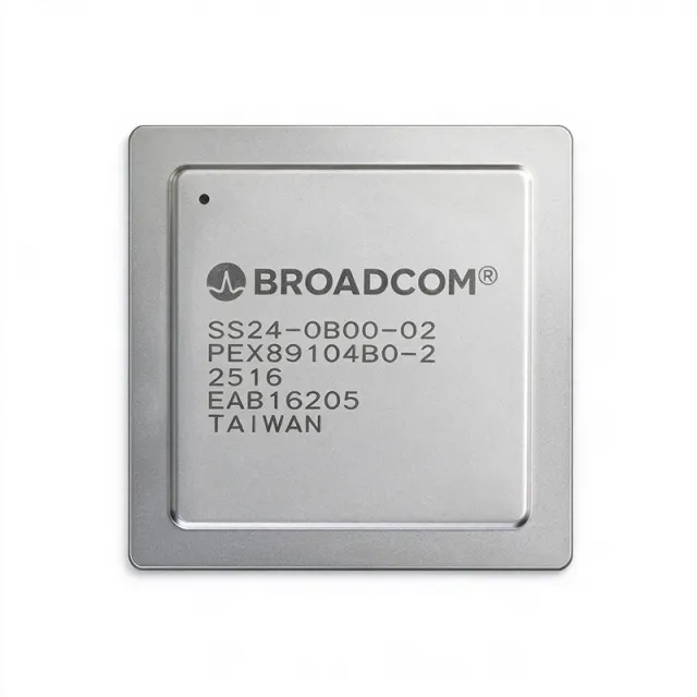
SS24-0B00-02 - 104-Lane PCIe 5.0 Switch | Broadcom PEX89000
The Broadcom SS24-0B00-02 is a 104-lane PCI Express 5.0 switch based on the Broadcom / Avago PEX89104B0-2-DB device, designed as an integrated, multi-function PCI Interface IC for high-performance server, storage, and accelerator fabrics. It is sold as a specialized PCI Interface component and serves as the silicon core used in Broadcom PEX89000-series evaluation boards and OEM modules. The part operates as a fan-out switching element with internal non-transparent and transparent bridge capability, enabling multi-host and domain partitioning topologies required by modern disaggregated compute designs. A PCI Express switch is a hot-pluggable, packet-routing device that sits between a root complex and one or more endpoints (or additional switches), forwarding Transaction Layer packets according to PCIe routing rules. SS24-0B00-02 belongs to the hierarchical product family PCIe switch -> PCI bridge / switch -> PCI Express switch -> peripheral / interface IC, and ultimately to integrated circuits -> specialized / interface ICs. The PCIe 5.0 specification doubles the per-lane signaling rate to 32 GT/s compared with PCIe 4.0, doubling bandwidth to roughly 3.94 GB/s per direction per lane. By aggregating 104 lanes, the switch can deliver multi-terabit fabric throughput and is engineered to support the higher port counts demanded by NVMe-oF, CXL-attached memory pools, and heterogeneous AI/GPU compute racks. Key features of the SS24-0B00-02 include PCIe 5.0 compliance with backward support for PCIe 4.0/3.0 devices, a 104-lane configuration organized into multiple ports, advanced error reporting and AER support, hot-plug readiness, NVMe and CXL-aware QoS structures, and support for SR-IOV and multiple function hierarchies. The silicon also includes Enhanced Hot-Plug controllers, ECRC, Poisoned TLP handling, and Advanced Power Management (ASPM L0s/L1/L2) capabilities typical of the PEX89000 generation. Architecturally, the device integrates SerDes blocks capable of PCIe 5.0 long-reach signaling, a non-blocking internal switch fabric with credit-based flow control, and embedded MCUs for I2C/SMBus manageability. The silicon targets enterprise servers, NVMe SSD arrays, GPU/CPU accelerator backplanes, and composable infrastructure platforms, where it typically appears as a stand-up PCIe card or a BGA-mounted mezzanine. Typical applications include high-port-count NVMe-oF SSD backplanes, disaggregated CXL memory pools, AI training cluster fabric switches, hyperscale accelerator baseboards, and high-speed test & measurement PCIe capture cards. When integrating this part, designers must follow Broadcom's reference layout for the BGA-EP package, manage the multi-rail power-up sequence, and provide sufficient airflow to dissipate the high SerDes power at PCIe 5.0 data rates. Engineers typically source the SS24-0B00-02 from authorized distributors such as DigiKey, Mouser, and Avnet Americas for new designs; later-stage replacement is sometimes supported by Broadcom via the cross-reference SS26-0B00-02 (60V equivalent) for higher-voltage tolerance retrofit programs. This page synthesizes distributor pricing, drop-in alternatives, and practical design notes not found in the manufacturer datasheet.
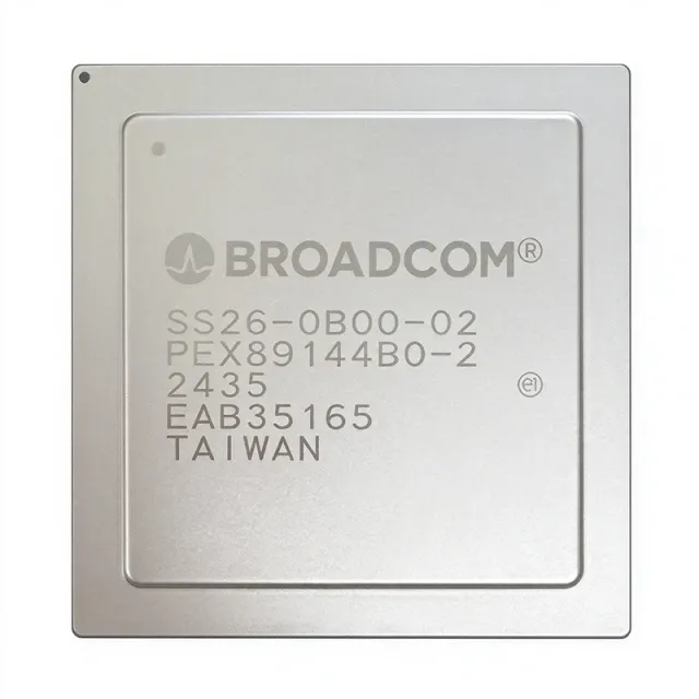
SS26-0B00-02 - PEX89144 PCIe Gen 5.0 Switch | Broadcom | 144-Lane
The Broadcom SS26-0B00-02 (associated die: PEX89144) is a 144-lane PCI Express 5.0 switch IC operating at 32 GT/s per lane, designed for high-end server, storage, and AI/ML fabric interconnects. As a member of the PEX89000 family of managed PCIe Gen 5.0 switches, it enables fan-out, partitioning, and non-transparent bridging across a heterogeneous set of root complexes and endpoints in modern accelerated-compute platforms. The part is supplied as a bare-die / specialized Broadcom package designated "SS26" and is targeted at OEM designs that integrate directly onto high-speed signal substrates. A PCIe switch is a protocol-aware layer-2 bridge device that replicates the PCI Express transaction layer and link layer across multiple ports, allowing one or more host processors to share a fabric of endpoints (NVMe SSDs, GPUs, NICs, accelerators) without requiring every device to live behind a single root complex. PCIe Gen 5.0 doubles the per-lane signaling rate to 32 GT/s versus Gen 4.0's 16 GT/s, doubling available bandwidth per lane to approximately 3.94 GB/s in each direction. Switches in this class sit within the broader taxonomy: PCIe switch -> PCIe interface IC -> peripheral controller -> integrated circuit -> semiconductor. Key features include 144 SerDes lanes arranged in 24 ports, support for hot-plug, surprise-down error reporting, Advanced Error Reporting (AER), SR-IOV with up to 256 physical functions per port, Multi-Root I/O virtualization (MR-IOV), and Broadcom's proprietary Adaptive Voltage Scaling / link-training diagnostics. The device integrates on-chip reference clocks, lane margining, and equalization controls required for Gen 5.0 signal integrity on long-reach backplane channels. Typical applications span hyperscale AI training fabrics where multiple GPUs share NVMe-oF storage, composable disaggregated servers, high-port-count NVMe SSD enclosures, and EBOF (Ethernet Bunch of Flash) reference platforms. The PEX89000 series extends Broadcom's PEX9700/8700/88000 lineage into Gen 5.0 territory, allowing customers to migrate existing Gen 3/4 designs with minimal firmware changes while doubling interconnect bandwidth. When designing with this device, follow Broadcom's PEX89000 hardware reference manual for PCB stackup, AC-coupling capacitor placement, and reference-clock routing. Always confirm lane assignment and bifurcation mode through the I2C/SMBus initial-provisioning interface before system bring-up.

ST3232BDR - 3.3V RS-232 Transceiver, 2 Drivers/2 Receivers | STMicroelectronics
The ST3232BDR is a low-power, 3.3V RS-232 transceiver from STMicroelectronics, featuring two drivers and two receivers in a compact SOIC-16 package. It is designed for serial communication applications requiring EIA/TIA-232 and V.28/V.24 compatibility, with a data rate of up to 400 kbps. The device operates from a single 3.0V to 5.5V supply, making it ideal for battery-powered and portable systems. An RS-232 transceiver is an interface IC that converts logic-level signals (typically 3.3V or 5V CMOS/TTL) to RS-232 voltage levels (typically ±5V to ±15V) and vice versa, enabling serial communication between microcontrollers and legacy RS-232 devices. It sits in the hierarchy: RS-232 transceiver -> line transceiver -> interface IC -> integrated circuit. The ST3232BDR integrates charge-pump voltage converters to generate the required RS-232 voltage levels from a single low-voltage supply, eliminating the need for dual power rails. Key features include a 3.0V to 5.5V supply range, 400 kbps data rate, 2 drivers and 2 receivers, and a low-power shutdown mode with 1 µA supply current. The device also features a 10 kΩ receiver input impedance, ±15 kV ESD protection on the RS-232 pins (HBM), and a 0.1 µF external capacitor requirement for the charge pump. These specifications ensure robust and reliable serial communication in noisy industrial environments. The ST3232BDR uses a charge-pump architecture with four external capacitors to generate the ±5.5V RS-232 voltage levels from the 3.3V supply. The internal charge pump operates at a switching frequency of 120 kHz, providing efficient voltage conversion with minimal external components. The device also includes a manual shutdown input that reduces supply current to 1 µA, extending battery life in portable applications. Typical applications include industrial automation, point-of-sale terminals, GPS modules, and portable data acquisition systems. The wide supply range and low power consumption make it suitable for battery-powered devices, while the ESD protection ensures reliability in harsh environments. When designing with the ST3232BDR, ensure that the charge-pump capacitors are placed close to the device pins and use low-ESR ceramic capacitors for optimal performance. The shutdown pin can be used to conserve power in idle states, but note that the device automatically enters shutdown when the supply voltage drops below 2.7V.
ST3232EBDR - 3.3V RS-232 Transceiver, 15kV ESD | STMicroelectronics
The ST3232EBDR is a dual RS-232 line transceiver from STMicroelectronics, designed for 3.3V to 5V supply operation. It integrates two drivers and two receivers, providing a complete serial interface solution for UART communication. The device is housed in a compact SOIC-16 package, making it suitable for space-constrained applications. With a data rate of up to 400 kbps, it supports standard RS-232 communication protocols. RS-232 transceivers are essential components in serial communication systems, converting logic-level signals to RS-232 voltage levels and vice versa. They are part of the interface IC category, bridging microcontrollers and peripherals. The ST3232EBDR operates from a single 3.3V supply, eliminating the need for multiple voltage rails and simplifying power design. Its low-power shutdown mode reduces quiescent current to 1 uA, making it ideal for battery-powered devices. Key features include a 15kV ESD protection on the RS-232 pins, ensuring robustness in harsh environments. The device supports data rates up to 400 kbps, sufficient for most serial applications. It includes an internal charge pump that generates the required ±5.5V RS-232 voltage levels from a single 3.3V supply, eliminating the need for external dual supplies. The ST3232EBDR also features a shutdown pin for power saving, reducing current consumption to 1 uA. Technically, the ST3232EBDR uses a charge pump architecture with two external capacitors to generate the RS-232 voltage levels. The device is designed to meet EIA/TIA-232E and ITU-T V.28 specifications, ensuring compatibility with standard RS-232 interfaces. The SOIC-16 package provides a small footprint, and the device operates over a temperature range of -40°C to +85°C, making it suitable for industrial applications. Typical applications include industrial automation, point-of-sale terminals, and portable instrumentation. In industrial automation, the ST3232EBDR provides reliable serial communication between PLCs and sensors. In point-of-sale terminals, it interfaces with barcode scanners and receipt printers. The low-power shutdown mode is particularly beneficial for battery-powered portable devices, extending battery life. When designing with the ST3232EBDR, ensure proper decoupling with a 0.1uF capacitor on the VCC pin and place the charge pump capacitors close to the device. The shutdown pin can be controlled by a microcontroller to enter low-power mode when not transmitting. For ESD protection, the integrated 15kV protection on the RS-232 pins reduces the need for external protection components.

ST3243ECTR-E - 3V-5.5V RS-232 Transceiver | STMicroelectronics
The STMicroelectronics ST3243ECTR-E is a 3-driver/5-receiver RS-232 transceiver with integrated ±15kV ESD protection, operating from a 3V to 5.5V single supply and housed in a 28-pin TSSOP (0.001 × 0.001 mm) tape-and-reel package. It supports data rates up to 400 kbps, includes a dual charge-pump circuit that generates the required RS-232 voltage levels (±5.5V) from a single supply rail, and features an auto power-down function for battery-powered applications. The device meets EIA/TIA-232 and V.28/V.24 communication standards. An RS-232 transceiver is a line driver/receiver IC that translates logic-level (typically 0 V / 3.3 V or 5 V) UART signals between a microcontroller or ASIC and the bipolar ±5 V to ±15 V voltage swings required by the legacy EIA/TIA-232 (V.28) serial communication standard. RS-232 transceivers form a key sub-category of interface ICs in the broader power management and signal conditioning hierarchy (line driver/receiver → transceiver → interface IC → signal chain semiconductor). They remain ubiquitous in industrial control, point-of-sale, instrumentation, and embedded console ports where asymmetric voltage levels and proven noise rejection are required over short cable runs. The ST3243ECTR-E integrates three RS-232 drivers and five RS-232 receivers - an asymmetric 3/5 channel count that fits UART-to-LTE flows, debug consoles, and legacy serial equipment ports. ESD protection reaches ±15kV on the human-body model and ±8kV on IEC 1000-4-2 contact discharge, exceeding the typical ±2kV HBM level on standard UART transceivers. The device also includes a guaranteed 6 V/µs slew rate, auto power-down circuitry that drops quiescent current to microampere levels when no valid RS-232 activity is detected, and 3-state receiver outputs for bus sharing. Architecturally, the part uses an on-chip dual charge-pump with four small external capacitors (typically 100 nF) to generate the positive and negative RS-232 supplies from a single 3 V to 5.5 V rail. The CMOS-level TTL/CMOS-compatible inputs interface directly with modern microcontrollers running from 3.3 V or 5 V without level shifters. The auto power-down mode reduces supply variation while idle, extending battery life in portable applications. Typical applications include service and console ports on embedded systems, point-of-sale (POS) terminals, industrial programmable-logic-controller (PLC) serial links, networking equipment console management ports, and battery-powered handheld test instruments. The wide 3 V to 5.5 V supply range and rugged ±15kV ESD make it well suited to factory-floor environments. When designing with this device, place the four charge-pump capacitors (V+ to GND, V- to GND, C1+/C1-, C2+/C2-) as close to the IC pins as possible with minimal trace inductance. Decouple VCC with a 0.1 µF ceramic capacitor. Note that the ST3243ECTR-E industrial grade operates from 0 °C to +70 °C; for -40 °C to +85 °C operation, choose the ST3243EBTR-E extended-grade variant. This page synthesizes distributor pricing, drop-in alternatives, and practical design notes not found in the manufacturer datasheet.
ST485CDR - 2.5Mbps Low-Power RS-485/RS-422 Transceiver SOIC-8 | ST
The STMicroelectronics ST485CDR is a low-power RS-485/RS-422 transceiver housed in an 8-pin SOIC (SO-8) package, supporting half-duplex communication with one driver and one receiver on a single differential pair. The part operates from a single 4.75V to 5.25V supply, draws 300 uA typical supply current when unloaded or with disabled drivers, and supports data rates up to 2.5 Mbps, making it suitable for high-speed industrial networks while keeping quiescent draw extremely low. An RS-485 transceiver is a differential line driver/receiver IC that translates between a single-ended UART/logic signal and the balanced twisted-pair signaling required by the TIA/EIA-485-A and TIA/EIA-422-B standards. RS-485 supports multi-drop (up to 32 transceivers on one bus) and half-/full-duplex topologies over cable runs of 1200 m, while RS-422 supports dedicated point-to-point or multi-drop simplex links. Within the broader signal-chain taxonomy, RS-485 transceivers are a subset of line transceivers -> interface ICs -> wired communication ICs. Key features include 2.5 Mbps data rate, 300 uA typical supply current, -7V to +12V common-mode range on the bus pins, internal current limiting on driver outputs, and thermal-shutdown protection that disables the driver if junction temperature exceeds safe limits. The receiver input hysteresis of 70 mV (typical) rejects line noise on long cable runs, and the 1/8-unit-load (or higher) input impedance permits multiple devices on a shared bus with minimal loading. The ST485CDR uses a bipolar CMOS-compatible driver architecture with slew-rate-controlled output transitions, which limits radiated EMI and reduces reflections on unterminated stubs. The chip is built on a BiCMOS process that delivers RS-485 drive strength (driver short-circuit current limited) while keeping quiescent draw at hundreds of microamperes, several orders of magnitude below legacy bipolar-only designs. Typical applications include industrial fieldbus links (Modbus RTU, PROFIBUS segments), building automation (BACnet MS-TP, DMX-512 lighting), point-of-sale peripherals, and any MCU UART extension over long cables. The low quiescent current also suits battery-backed monitoring nodes where the bus is idle for long periods. Designers should provide a 100 nF decoupling capacitor within 5 mm of VCC and add a 100 ohm termination resistor at each end of long runs to suppress signal reflections. The DE and RE pins can be tied together for simplex operation, or driven separately for direction-controlled half-duplex buses. This page synthesizes distributor pricing, drop-in cross-brand alternatives, and PCB layout notes not collected in the manufacturer datasheet alone, giving engineers a faster path from datasheet search to BOM placement.

ST75185CTR - 3.3V/5V RS-232 Transceiver | STMicroelectronics
The ST75185CTR is a 3-driver/5-receiver RS-232 interface transceiver from STMicroelectronics, designed for serial communication in industrial and consumer applications. It operates from a single 3.3V or 5V power supply, with an integrated charge pump that generates the required ±10V RS-232 voltage levels. The device is available in a 20-pin SOIC (SOP-20) package, providing a compact solution for space-constrained designs. RS-232 transceivers are a type of serial communication interface IC that converts logic-level signals (typically 3.3V or 5V) to RS-232 voltage levels (±5V to ±15V) and vice versa. They are part of the broader interface IC category, which also includes UARTs, USB transceivers, and CAN transceivers. RS-232 transceivers are essential for legacy serial communication with PCs, industrial equipment, and test instruments, where the RS-232 standard (EIA-232) is still widely used. Key features of the ST75185CTR include a data rate of up to 120 kbps, which is sufficient for most RS-232 applications, and an ESD protection of ±2 kV (HBM) on the RS-232 pins, ensuring robustness in harsh environments. The device also features a low-power shutdown mode that reduces quiescent current to 1 µA, making it suitable for battery-powered or power-sensitive applications. The charge pump requires only four external 0.1 µF capacitors, simplifying the PCB layout. The ST75185CTR uses a dual charge pump architecture to generate the positive and negative supply rails from a single 3.3V or 5V input. This eliminates the need for a separate negative supply, reducing system cost and board space. The device is designed to meet the EIA-232 and ITU-T V.28 standards, ensuring interoperability with standard RS-232 devices. Typical applications include industrial automation, point-of-sale (POS) terminals, data acquisition systems, and embedded systems requiring serial communication. The wide operating temperature range of -40°C to +85°C makes it suitable for industrial environments. The device is also used in networking equipment, such as routers and switches, for console management ports. When designing with the ST75185CTR, ensure that the charge pump capacitors are placed close to the device pins to minimize noise and ripple. The shutdown pin can be used to reduce power consumption when the transceiver is idle. For ESD protection, the device provides ±2 kV HBM on the RS-232 pins, but additional external protection may be required for applications with higher ESD exposure.

STA304A - 6-Channel Digital Audio Processor | STMicroelectronics
STMicroelectronics STA304A is a fully integrated, 6-channel digital audio processor with I2C and I2S interfaces, a 3 V to 3.6 V supply range, and a 44-TQFP 10 mm by 10 mm package. It belongs to STMicroelectronics' DDX family of digital audio processors and is designed to provide centralized digital signal processing for multichannel audio systems. The verified product data identifies the device as obsolete, so new production procurement should be treated as constrained. A digital audio processor is a specialized integrated circuit that receives, processes, and distributes digital audio signals within an audio system. In the broader product hierarchy, the STA304A is an audio processor, which is a form of audio special-purpose IC and therefore part of the wider semiconductor and signal-processing ecosystem. Its I2C interface supports control and configuration, while its I2S interface supports serialized digital audio data transfer. The STA304A provides six digital audio channels in one integrated device. This channel count allows one processor to coordinate multichannel audio routing and processing rather than requiring a separate discrete solution for each channel. Its 3 V to 3.6 V operating supply range allows integration into compatible 3.3 V audio equipment. The 44-TQFP surface-mount package provides a compact solution for multichannel consumer audio products. The device combines digital audio processing, control connectivity, and multichannel interface functionality in a single package. According to the verified STMicroelectronics product information, its supported interfaces are I2C and I2S. I2C is useful for configuration and register access, while I2S carries digital audio samples between the processor and codecs, amplifiers, converters, or other digital audio endpoints. Typical uses include active speakers, multichannel home-audio equipment, digital mixing equipment, and other consumer audio systems that require centralized multichannel processing. In an I2S audio path, the STA304A can sit between a digital audio source and one or more audio codecs. The supplied product information does not specify sample rate, processing latency, channel mapping, or output-routing details, so those characteristics must be confirmed in the manufacturer datasheet before design release. Engineers should pay particular attention to the obsolete lifecycle status and validate interface timing, power sequencing, and channel assignment against the manufacturer documentation. Because the verified information identifies the part as obsolete, boards requiring long-term availability may need an approved redesign rather than a routine procurement substitution. Any replacement should be evaluated for package, pinout, supply voltage, I2C behavior, and I2S signal compatibility. This product record combines verified distributor and manufacturer-linked information with practical sourcing, design, and replacement guidance. It distinguishes confirmed STA304A characteristics from parameters that remain unavailable, helping engineers make informed decisions without treating an unverified alternative as a guaranteed drop-in replacement.

STA30813TR - 8-Channel 24-Bit DDX Audio Processor | STMicroelectronics
The STMicroelectronics STA30813TR is an eight-channel multichannel digital audio processor with DDX processing, 24-bit operation, and support for input sample rates from 192 kHz down to the audio-band rates supported by the device family. The processor is packaged in a 64-lead TQFP measuring 10 x 10 mm and is intended for tone control, preamplification, and multichannel audio signal processing. An audio processor is a specialized signal-processing IC that applies gain, volume, filtering, and other control functions to multiple digital audio channels. Within the signal-chain hierarchy, it sits between an audio ADC or digital audio source and a DAC or power-amplifier stage. Instead of using one external preamplifier per channel, an integrated processor can centralize control across eight channels and reduce the number of external analog-control components. The STA30813TR provides eight 24-bit DDX channels, a variable digital gain range of 24 dB in 0.5 dB steps, and volume control in 0.5 dB steps. A digital limiter function helps control signal excursions. These features make the device applicable to multichannel preamplifiers, active speaker systems, home-theater audio, and professional audio equipment requiring coordinated channel-level adjustment. Its multichannel architecture allows common processing parameters to be applied across several audio paths. Digital gain and volume adjustments can be performed after conversion into the digital domain, which helps keep channel balance consistent and reduces sensitivity to component tolerance compared with purely analog gain control. The exact supported interface modes and configuration options should be confirmed in the manufacturer datasheet before layout is finalized. Typical uses include digital preamplifier boards, eight-channel mixer modules, powered-speaker control boards, surround-sound systems, and audio receiver or amplifier subsystems. The 10 x 10 mm TQFP package keeps the device compact while exposing enough pins for digital audio connections, control signals, clocking, power, and configuration functions. When designing around this obsolete device, verify every pin assignment, supply requirement, interface mode, and clock configuration against the original manufacturer datasheet. Board bring-up should also confirm the expected DDX behavior and limiter settings, particularly when the processor sits in a high-gain or live-signal path. This page consolidates the confirmed channel-count, bit-depth, gain, volume-control, packaging, and temperature information, while separating confirmed drop-in references from options that require additional compatibility verification. It also provides design guidance and application context that are not present in a basic distributor listing.

STA310 - 6+2-Channel Audio Decoder | STMicroelectronics
The STMicroelectronics STA310 is a fully integrated multistandard audio decoder with 6+2-channel decoding, designed for HDTV, audio players, receivers, and set-top boxes in an 80-pin TQFP (14x14) package. The supplied data confirms support for DVD Audio Meridian Lossless Packing (MLP), uncompressed LPCM with 1–8 channels, and encoded data input through serial I2S, S/PDIF, or parallel interfaces. An audio decoder is an interface IC that converts compressed or encoded digital audio streams into PCM data for downstream digital-to-analog converters, amplifiers, receivers, or speakers. Within the signal chain, it sits between a source interface and the audio output stage, handling format recognition, channel organization, and decoding while leaving analog amplification and loudspeaker drive to downstream components. The STA310's key verified features include integrated multistandard decoding and support for both serial and parallel input paths. The I2S and S/PDIF options suit modern digital audio systems, while the parallel interface can support legacy source architectures. Its 6+2-channel capability is relevant to multichannel home entertainment, although exact channel-routing behavior must be confirmed from the manufacturer datasheet and application implementation. The architecture combines encoded digital audio input, format-specific decoding, and decoded audio output in one device. This integration can reduce the external decoder count in a set-top box, DVD player, HDTV, or surround-sound receiver. System designers must still account for clocking, supported sample rates, output format, electrical levels, signal integrity, and software or control requirements that are not specified in the supplied web excerpts. Typical applications include HDTV audio processing, DVD and disc-player output stages, AV receivers, digital audio players, set-top boxes, and other home-entertainment equipment. The STA310 is especially relevant where a product must accept encoded digital audio from several source types and produce decoded multichannel PCM audio for a downstream codec or amplifier. When laying out an STA310 design, preserve the exact pin assignments and reference interface timing shown in the manufacturer datasheet. Keep digital audio, clock, and power routing controlled, provide the required bypass and interface components, and validate timing margins across every supported input format. This page consolidates distributor identification, verified format support, sourcing data, and engineering guidance.
STB-835 - AN & DIG Panel for I/O | Analog Devices
The Analog Devices STB-835 is an analog and digital panel for I/O, classified by LCSC as an Interface - Specialized integrated circuit. The verified listing identifies the MPN as STB-835 and the manufacturer as Analog Devices, while the available distributor records provide sourcing information rather than a complete electrical datasheet. The supplied listing does not establish the package, pin count, supply-voltage range, signal count, operating temperature, or environmental ratings; those parameters must be confirmed from the manufacturer documentation before design release. An interface IC is a semiconductor that connects a controller, panel, test fixture, or external circuit through analog and digital signal paths. A panel-for-I/O device commonly organizes input and output functions into a defined interface structure, allowing a system to monitor or control external lines through a standardized connection arrangement. Unlike a general-purpose logic IC, a specialized interface panel may combine input conditioning, output drivers, isolation, or panel-specific routing, but the exact functions of STB-835 are not available in the supplied verified records. The strongest verified product facts are the manufacturer identity, the functional description “AN & DIG PANEL FOR I/O,” the Interface - Specialized classification, and the listed commercial availability. LCSC reports the part as in stock and states a price from $61.5230 as of the supplied 2026-10-23 search timestamp. DigiKey, JLCPCB, Octopart, Cytech Systems, and other listings provide purchasing or comparison entry points, but their snippets do not expose enough technical detail to populate electrical specifications without fabrication. STB-835 should therefore be treated as a procurement-qualified interface component with incomplete application-level characterization. Before placing it in a PCB design, obtain the official Analog Devices datasheet or approved Rochester Electronics documentation and verify the exact package drawing, pin names, signal directions, voltage domains, timing, power consumption, and environmental limits. The listed Rochester Electronics association may indicate legacy or specialty sourcing, but it does not establish lifecycle status, obsolete designation, or a direct replacement. Typical design work involves mapping every panel connection to the verified pinout, checking voltage-domain compatibility across connected analog and digital signals, and validating input thresholds and output drive capability before layout. Because no verified package or pinout is supplied, PCB footprint selection must not be inferred from distributor category data. This page distinguishes verified commercial information from missing technical data so procurement and engineering teams can identify the next required verification step. This page combines verified distributor availability, pricing, sourcing links, and explicit data gaps with engineering guidance for evaluating a specialized interface panel. It intentionally avoids guessing pin assignments, electrical limits, lifecycle claims, compliance status, or substitute parts that could create an unsafe PCB redesign.
STB-BB05 - RTI204/205 Interface Panel IC | Analog Devices
The Analog Devices STB-BB05 is an RTI204/205 interface-panel integrated circuit offered in bulk packaging. The verified listing identifies it as an Analog Devices component associated with the Telecom & Specialized integrated-circuit family, while one distributor record categorizes it as a Specialized interface IC. Its exact electrical ratings, pin arrangement, and mechanical dimensions are not exposed in the supplied sources. The available catalog information instead confirms the device identity, manufacturer association, interface-panel role, bulk order form, and sourcing status. Engineers should therefore treat this page as a procurement and identification resource rather than a substitute for the original manufacturer documentation. An interface-panel IC is a type of integrated circuit that connects external equipment, control signals, or peripheral circuitry to a system interface. In the telecommunications and specialized-equipment hierarchy, such a device sits between discrete connectors and higher-level communication electronics: connectors provide the physical path, the interface IC conditions or translates signals, and the host system performs control and data processing. The supplied distributor description associates STB-BB05 specifically with RTI204/205 interface-panel applications, making those panel functions the central application context. The available evidence confirms the MPN STB-BB05, Analog Devices branding, specialized-interface classification, and bulk packaging. One supplier lists a minimum order quantity of 2, while other listings direct buyers to submit an RFQ to confirm stock, date code, and lead time. A Rochester Electronics record reports the component as active. These facts make STB-BB05 potentially relevant to repair, maintenance, replication, and legacy-system support, but production use still requires confirmation of environmental ratings, supply conditions, and pin compatibility. Technically, the available data does not identify whether the device is a surface-mount or through-hole part. Rochester Electronics lists mounting type and package as unavailable, while another supplier describes the shipment format as Bulk. Because the exact package is unknown, no package-specific land pattern, pinout diagram, thermal calculation, or drop-in replacement claim can be supported. This uncertainty is especially important for proprietary interface hardware, where similar connector functions do not guarantee signal-level or timing compatibility. Typical sourcing uses for STB-BB05 include RTI204/205 interface-panel maintenance, specialized telecommunications equipment repair, legacy system restoration, and component matching during low-volume production. For each use, the engineer should verify the original equipment schematic, pin connections, supply requirements, logic levels, and timing before installation. The listing supports component identification and RFQ-based procurement, but does not provide enough technical data to establish those electrical requirements independently. The principal design consideration is to avoid assuming compatibility from the RTI204/205 description alone. Before procurement, request the manufacturer datasheet, drawing, revision status, and inspection information from the supplier or original equipment manufacturer. Also confirm whether the offered unit is an original packaged component, a screened assembly, or an alternate-source item. These checks are essential because a catalog listing can confirm identity and sourcing availability without confirming electrical equivalence or manufacturing provenance. This page consolidates the supplied distributor identities, lifecycle statement, interface classification, package uncertainty, and procurement references. It intentionally avoids fabricating electrical values, pin names, package dimensions, pricing, or cross-references that were absent from the verified sources.
STB-GP - RT1850/RT1860 Panel | Analog Devices | Telecom
The Analog Devices STB-GP is a specialized interface panel identified for use with RT1850 and RT1860 assemblies, available from distributors as an active or in-stock component. The verified product listing identifies STB-GP as “PANEL FOR RT1850 RT1860,” while Rochester Electronics describes the device as belonging to the Telecom & Specialized integrated-circuit family. Its public listing does not provide a conventional IC package, pinout, electrical ratings, interface protocol, or mounting data, so those details remain unverified rather than inferred. The STB-GP designation therefore should be treated as a specialized panel or module-related procurement item until the manufacturer documentation is obtained. A specialized interface IC or panel is used to connect, route, adapt, or terminate signals within a larger telecom, networking, or embedded system. The STB-GP listing connects this item with RT1850 and RT1860, which are identified by the source data as related assemblies, but the exact electrical role, signal directions, connector arrangement, and supported system configuration are not provided. Engineers should therefore confirm the system revision and board connector before ordering or substituting it. The available commercial evidence indicates availability rather than a complete technical datasheet. LCSC lists STB-GP as in stock with a starting price of $69.6681, eBee lists a starting price of $73.2624, and Rochester/FPGACenter lists a starting unit price of $146.99 with volume discounts for quantities of 10, 100, 500, and 1,000. Prices are reproduced as reported and may change without notice as of 2026-10-23. Octopart also lists Analog Devices STB-GP and directs buyers to compare bulk pricing and availability. Because the verified sources do not specify package dimensions, pin count, mounting type, operating temperature, voltage, current, RoHS, REACH, or automotive qualification, this page does not invent those values. The procurement-critical decision is compatibility with the intended RT1850/RT1860 assembly, not an assumed generic IC replacement. Request the current Analog Devices or Rochester Electronics documentation, mechanical drawing, and revision information before using the part in a new design. This page combines verified distributor identity, reported pricing, lifecycle information, sourcing links, and explicit data gaps. It is intended to help engineers identify STB-GP quickly while preventing unsupported assumptions about electrical compatibility, package fit, or drop-in replacement.