EP2S15F484C4 vs EP2S15F484C5 Ikinahambing
Detalyadong pagkakahiwalay na pagkakahambing ng EP2S15F484C4 sa pamamagitan ng Intel at EP2S15F484C5 sa pamamagitan ng Intel. Ikinahambing ang mga pangunahing paglalarawan, mga tama ng elektriko, paakay, kalagayan ng buhay, presyo, at pagkakaroon upang makita ang pinakamahusay na komponente para sa iyong mga kinakailangang pang disenyo.
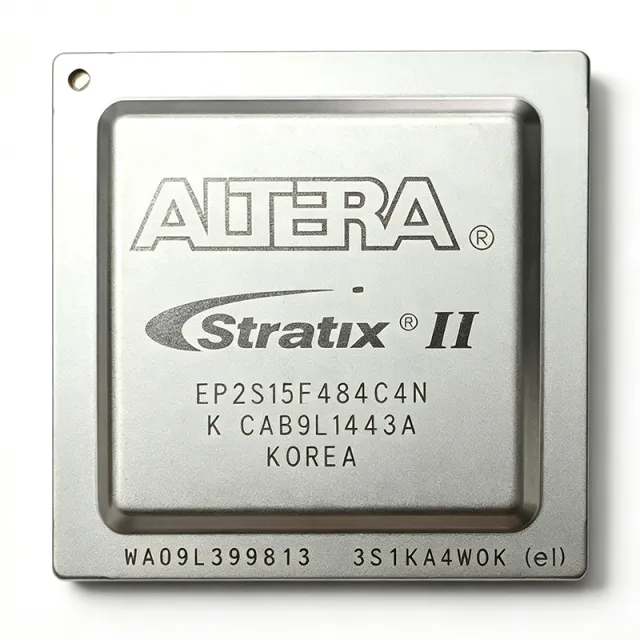

Pagsanggunian na paghahambing
| Parametro | EP2S15F484C4 | EP2S15F484C5 |
|---|---|---|
| Brand | Intel | Intel |
| Kategorya | FPGA & CPLD | FPGA & CPLD |
| Katayuan ng Lifecycle | Huling Pagbili | Obsolete |
| Presyo ng Yunit (USD) | $205.00 | — |
| Family | Stratix II | Stratix II |
| Logic Elements (LEs) | 15,600 | — |
| Adaptive Logic Modules (ALMs) / CLBs | 6,240 | — |
| Embedded Memory (Bits) | 419,328 | — |
| Maximum User I/O | 342 | — |
| DSP Blocks | Yes (integrated multiplier-accumulators) | — |
| Packhaging | 484-FBGA (FBGA-484) | 484-ball FBGA (FC-FBGA) |
| Package Dimensions | 23 mm x 23 mm | — |
| Ball Pitch | 1.0 mm | — |
| Process Technology | 90 nm CMOS | — |
| Core Performance | Up to 717 MHz | — |
| Speed Grade | C4 (-4, mid-tier) | — |
| Temperature Grade | Commercial (C): 0 C to +85 C junction | — |
| Supply Voltage (Core) | [DATA_NEEDED: VCCINT nominal] | 1.2 V |
| I/O Standards Supported | LVDS, LVTTL, LVCMOS, SSTL, HSTL | — |
| External Memory Interface | DDR, DDR2, QDR SRAM | — |
| Configuration Method | Serial/parallel, JTAG | SRAM-based (volatile, external config device) |
| Tindminan RoHS | Compliant (lead-free FBGA package) | Non-Compliant (Contains Lead) |
| Logic Elements (LE) | — | 15,600 |
| Adaptive Logic Modules (ALMs) | — | 6240 |
| LABs / CLBs | — | 780 |
| Embedded Memory | — | 409 Kbit (TriMatrix) |
| User I/O Count | — | 342 |
| Number of Logic Cells | — | 15600 |
| Maximum Operating Frequency | — | 609.76 MHz |
| Uri ng Pagpapasok | — | Surface Mount |
| Process Node | — | 90 nm |
| Operating Temperature Grade | — | Commercial (per DigiKey listing) |