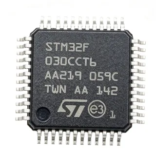
LPC2468FET208K - 72MHz ARM7 MCU with 512KB Flash | NXP
MPN: LPC2468FET208K ✓ NakahandaLPC2468FET208K Ulas
A microcontroller is an integrated semiconductor device containing a processor core, memory, peripherals, and interface logic on one die. The LPC2468 belongs to the ARM7 microcontroller hierarchy, where ARM7TDMI-S combines a 32-bit RISC processor with Thumb instruction support. This combination gives the device both 16-bit and 32-bit execution capabilities while providing dedicated Ethernet, CAN, USB, and real-time debug resources within a single package.
The principal features of the LPC2468FET208K include a 72 MHz maximum clock, 512 KB of high-speed on-chip flash, and 100,352 bytes of on-chip RAM. Its communications block supports Ethernet, CAN, and USB 2.0 device, host, and OTG operation. The controller also provides ISP and IAP capabilities for in-system or in-application programming, while JTAG and embedded trace support board-level debugging and real-time trace analysis.
The LPC2468 is built around the 16-bit/32-bit Arm7TDMI-S RISC core, with a 24-bit address bus and 160 I/O lines. Its 3.3 V operating supply and extensive on-chip connectivity suit embedded control platforms that need more than a basic processor. Ethernet, CAN, and USB interfaces allow the same device to bridge wired networking, industrial communication, and USB host or peripheral functions without requiring several discrete interface controllers.
Typical applications include industrial Ethernet controllers, CAN-connected factory equipment, USB-to-embedded bridges, networked industrial control units, medical equipment, and communications infrastructure. The 208-pin TFBGA package provides access to the wide peripheral and I/O set, while the integrated debug architecture helps developers diagnose timing-sensitive firmware and communication issues directly on the target board.
Designers should verify the complete pin assignment and exposed-pad requirements in the manufacturer datasheet before layout release. Decoupling, high-speed signal integrity, ground-plane continuity, and external-memory routing are especially important in a 208-pin ball-grid-array design. Confirm the PCB stack-up and escape-routing strategy against the package drawing rather than inferring connectivity from the commercial part description.
This product page organizes the verified LPC2468FET208K specifications, package information, connectivity features, application guidance, and sourcing workflow. It also distinguishes published parameters from values that still require confirmation from the official LPC2468 datasheet, helping engineers make a technically defensible design decision.
Mga alternatibo na pwedeng ilagay na LPC2468FET208K — parehas na package, pin-to-pin na katugmang. Hindi kasama ang mga bahagi ng iba't-ibang package na nangangailangan ng pagpapaayos ng PCB.
Wala ng magagamit na drop-in alternatibo para sa produkto na ito.
Hilingin ang AlternatiboLPC2468FET208K Mga Pinakamataas na Rating at Electrical Characteristics
| CPU Core | ARM7TDMI-S |
| Architecture | 16-bit/32-bit |
| Maximum CPU Frequency | 72 MHz |
| On-Chip Flash Memory | 512 KB |
| On-Chip RAM | 100352 bytes |
| Address Bus Width | 24-bit |
| I/O Lines | 160 |
| Operating Supply | 3.3 V |
| Ethernet Interface | Integrated Ethernet |
| CAN Interface | Integrated CAN |
| USB Interface | USB 2.0 device, host, and OTG |
| Programming Interfaces | ISP and IAP |
| Debug Interfaces | JTAG and embedded trace |
| External Memory Interface | Integrated external memory interface |
| Packhaging | 208-pin TFBGA, 15 mm × 15 mm |
| Uri ng Pagpapasok | Surface Mount |
| Manufacturer Qualification | Medical |
Gabay sa Pin Configuration ng LPC2468FET208K 208-pin tfbga, 15 mm × 15 mm
Pin configuration para sa LPC2468FET208K (208-pin tfbga, 15 mm × 15 mm package). Kasama sa digital IC na ito ang GPIO, mga communication interface (UART, SPI, I2C), at mga power pin. Sumangguni sa datasheet ng manufacturer para sa mga alternatibong function ng pin at mga opsyon sa configuration. Mahalaga para sa disenyo ng embedded system at PCB layout.

Wala ng detalyadong pinout data na magagamit para sa LPC2468FET208K.
Sumangguni sa datasheet para sa buong pin configuration.
Tipikal na mga Gamit
LPC2468FET208K ay nararapat para sa 6 aplikasyons: Industrial Ethernet Control, USB-to-Embedded Bridge, CAN-Connected Equipment, Industrial Gateway, Medical Device Controller, Communication Infrastructure.
Industrial Ethernet Control
The LPC2468FET208K fits industrial Ethernet controllers because it combines a 72 MHz ARM7TDMI-S processor with integrated Ethernet, 512 KB of flash, and 100,352 bytes of RAM. The MCU can coordinate machine controls, network management, status reporting, and local service interfaces without requiring a separate network controller. Its 160 I/O lines and external memory interface leave room for sensors, actuators, and larger data buffers. The main design concern is validating Ethernet timing, isolation requirements, and the thermal performance of the 208-pin TFBGA layout in the final enclosure.
USB-to-Embedded Bridge
The LPC2468FET208K is suitable for a USB-to-embedded bridge because USB 2.0 device, host, and OTG support is integrated alongside Ethernet, CAN, and extensive I/O. A bridge can expose storage, configuration tools, or field-service connections while maintaining additional wired communication paths. The 72 MHz ARM7TDMI-S core supports protocol handling, and 512 KB of flash provides room for boot code and application firmware. Designers must carefully route USB differential signals and validate connector, power, grounding, and enumeration behavior on the completed PCB.
CAN-Connected Equipment
Integrated CAN makes the LPC2468FET208K appropriate for equipment that participates in industrial or vehicle-style controller networks. The microcontroller can process sensor data, enforce control logic, exchange diagnostic messages, and coordinate service functions while retaining Ethernet and USB connectivity for configuration and monitoring. Its 72 MHz core and 100,352 bytes of RAM support multitasking and communication buffering, while the external memory interface permits additional storage where required. A production design should validate transceiver selection, termination, isolation, error recovery, and network timing.
Industrial Gateway
A multi-protocol industrial gateway benefits from the LPC2468FET208K because Ethernet, CAN, USB 2.0, external memory, and 160 I/O lines are available on one microcontroller. The architecture can bridge management networks to fieldbus equipment, support local data buffering, and expose USB maintenance access without combining several interface controllers. The 512 KB flash and 100,352 bytes of RAM provide a consolidated firmware platform for protocol conversion and diagnostics. Thermal analysis and careful segregation of communications and power domains are important in compact industrial enclosures.
Medical Device Controller
The LPC2468FET208K can serve as the controller in a connected medical device because it integrates Ethernet, CAN, USB 2.0, and deterministic microcontroller resources in a 3.3 V design. The 72 MHz ARM7TDMI-S core can coordinate control loops, data acquisition, operator interfaces, and communications, while ISP/IAP supports controlled firmware maintenance workflows. Its 160 I/O lines and external memory interface allow connection to sensors, displays, and storage. Medical use requires project-specific regulatory, safety, and qualification validation beyond the basic commercial part attributes.
Communication Infrastructure
The LPC2468FET208K suits communication infrastructure equipment requiring several peripheral standards and a broad external interface. Integrated Ethernet, CAN, and USB allow the same platform to manage network links, service connections, and embedded monitoring functions. Its 24-bit address bus and external memory interface support larger memory-mapped systems, while JTAG and embedded trace assist development and field diagnostics. The wide 208-pin TFBGA package increases routing and assembly complexity, so high-speed escape routing, plane continuity, thermal relief, and connector placement require careful PCB planning.
Impormasyon ng Talumpati sa Engineering for LPC2468FET208K — ikabit, gabay sa disenyo, at impormasyon ng pagsunod sa kautusan.
Paunawang Hanapin
Talaan ng Disenyo
Use the official LPC2468 package drawing and pin-description table to create the 208-ball TFBGA footprint. Confirm ball-pitch, pad geometry, solder-mask definition, paste stencil, exposed thermal requirements, and PCB tolerances before releasing manufacturing data. The product listings establish the 15 mm × 15 mm package but do not provide a complete land pattern, so board geometry should not be inferred from the commercial package name.
Plan continuous ground-plane distribution across the 208-pin TFBGA and minimize return-path interruptions beneath the device. Ethernet, USB, CAN, memory, and debug signals each require appropriate impedance and return-path planning. Place decoupling structures at the associated supply pins, keep sensitive analog or clock routes away from high-switching nets, and follow the manufacturer reference layout and external-component recommendations in the datasheet.
Do not assume that two LPC2468 order codes with similar names are firmware-identical. NXP Community information identifies LPC2468FET208K as silicon version 5 and LPC2468FET208,551 as version 15. Review device revisions, errata, peripheral behavior, startup code, and validated application notes before treating either version as an interchangeable substitute for an existing production design.
Impormasyon ng Pagsunod sa Kautusan
The listings identify the device as a medical-marketed 3.3 V MCU but do not state RoHS, REACH, lead-free, halogen-free, or conflict-minerals status. AEC-Q100 is not applicable because this is a general-purpose ARM7 microcontroller rather than an automotive-qualified part.