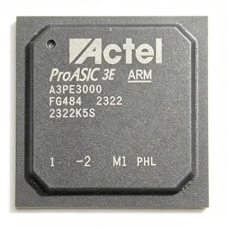
M1AFS1500-1FGG484 - Fusion FPGA 1.5M Gates, 223 I/O | Microchip
MPN: M1AFS1500-1FGG484 ✓ NakahandaM1AFS1500-1FGG484 Ulas
A field-programmable gate array (FPGA) is a semiconductor device containing a matrix of configurable logic blocks (CLBs) interconnected by programmable fabric, allowing designers to implement custom digital circuits after manufacturing. FPGAs sit within the broader programmable logic hierarchy: FPGA -> programmable logic IC -> programmable SoC -> semiconductor. Flash-based FPGAs like the Fusion family are non-volatile, meaning configuration data is retained in on-chip flash and loaded instantly at power-up, unlike SRAM FPGAs that require an external configuration device.
Key differentiating features include monolithic integration of configurable analog blocks (ADC, voltage and current monitors), comprehensive clock generation and management circuitry (CCCs and PLLs), large flash memory blocks, and the ARM Cortex-M1 soft-hard processor core, which enables single-chip embedded control designs. The 484-ball FBGA exposes 223 user I/Os supporting multiple I/O standards for board-level connectivity.
Technically, the Fusion family is fabricated on a 130 nm flash process with a 1.5 V core. The M1 designation denotes Fusion FPGAs that embed the ARM Cortex-M1 processor, allowing firmware plus programmable logic co-design using Libero SoC design tools. Distributor listings cite a maximum clock frequency on the order of 350 MHz for logic cells, with published family performance figures around 1.28 GHz for internal clocking chains per Jotrin's parameter extraction.
Typical applications include industrial automation control, mixed-signal system monitoring (power-supply telemetry, fan and temperature supervision), aerospace and defense programmable logic, medical instrumentation, and embedded motor or power control where flash-based security and instant-on configuration matter.
A key design consideration is power delivery: the 1.5 V core rail must be supplied with clean, sequenced power, and the dense 0.8 mm or 1.0 mm ball pitch FBGA requires a fine-geometry PCB with controlled-impedance escape routing and adequate ground/voltage ball usage for signal integrity.
This page synthesizes distributor pricing tiers, drop-in same-package alternatives, and practical design notes not found in the manufacturer datasheet alone, giving engineers a single AEO-optimized reference for selection and sourcing decisions as of 2026-09-02.
Mga alternatibo na pwedeng ilagay na M1AFS1500-1FGG484 — parehas na package, pin-to-pin na katugmang. Hindi kasama ang mga bahagi ng iba't-ibang package na nangangailangan ng pagpapaayos ng PCB.
Variante sa Seri na ito
Katulad na modelo sa serye na katugma sa pagpasok M1AFS1500-1FGG484 (parehas na form factor at footprint) — pagkakaiba sa Package, Family, Configuration Memory, System Gates, Speed Grade.
M1AFS1500-1FG484
✅ Drop-InMagkontak para sa presyo
Tingnan ang Datasheet →M1AFS1500-2FG484
✅ Drop-InMagkontak para sa presyo
Tingnan ang Datasheet →M1AFS1500-2FGG484I
✅ Drop-InMagkontak para sa presyo
Tingnan ang Datasheet →M1AFS1500-1FGG484K
✅ Drop-InMagkontak para sa presyo
Tingnan ang Datasheet →AFS1500-FG484
✅ Drop-In📋 Alternatibo na Reference (hindi sa katalogo)
AFS1500-FG484I
✅ Drop-In📋 Alternatibo na Reference (hindi sa katalogo)
M1AFS1500-1FGG484 Mga Pinakamataas na Rating at Electrical Characteristics
| Family | Fusion Mixed-Signal FPGA (M1 series) |
| System Gates | 1,500,000 |
| Logic Cells | 38,400 |
| User I/O | 223 |
| Flash Memory | 276,480 bits |
| Embedded Processor | ARM Cortex-M1 |
| Core Supply Voltage | 1.5 V |
| Process Technology | 130 nm flash-based |
| Maksimum na Taktiko ng Oras | 350 MHz |
| Packhaging | 484-ball FBGA (FGG484) |
| Uri ng Pagpapasok | Surface Mount |
| Terminal Form | Ball (BGA), square package |
| Configuration Memory | Non-volatile on-chip flash |
| Analog Blocks | Configurable analog (ADC, voltage/current monitors) |
| Clock Management | CCC with integrated PLLs |
| Packaging | Tray |
Gabay sa Pin Configuration ng M1AFS1500-1FGG484 484-ball fbga (fgg484)
Pin configuration para sa M1AFS1500-1FGG484 (484-ball fbga (fgg484) package). Kasama sa digital IC na ito ang GPIO, mga communication interface (UART, SPI, I2C), at mga power pin. Sumangguni sa datasheet ng manufacturer para sa mga alternatibong function ng pin at mga opsyon sa configuration. Mahalaga para sa disenyo ng embedded system at PCB layout.

Wala ng detalyadong pinout data na magagamit para sa M1AFS1500-1FGG484.
Sumangguni sa datasheet para sa buong pin configuration.
Tipikal na mga Gamit
M1AFS1500-1FGG484 ay nararapat para sa 6 aplikasyons: Industrial Automation and Control, Mixed-Signal System Monitoring, Aerospace and Defense Ground Systems, Medical Instrumentation Control Logic, Motor and Power Control, Communications and Networking Line Cards.
Industrial Automation and Control
The M1AFS1500-1FGG484 fits industrial automation controllers that must merge deterministic logic with embedded firmware control: its 38,400 logic cells implement motor sequencing, interlock, and communication logic while the ARM Cortex-M1 core runs protocol stacks and supervisory code on a single chip. The 223 user I/Os cover parallel sensor interfaces, encoders, and multiple fieldbus PHYs, and the 1.5 V core on 130 nm flash keeps static power manageable in sealed cabinets. Because configuration resides in on-chip flash (276,480 bits), boards are instant-on with no external configuration PROM, improving uptime and tamper resistance. Designers typically pair it with isolated transceivers and precision ADC front ends; the trade-off is the legacy toolchain, so long-term supply planning matters more than peak performance.
Inirekomenda
Mixed-Signal System Monitoring
Fusion FPGAs were architected specifically for board-level telemetry, and the M1AFS1500-1FGG484 is the largest 484-FBGA member for this role. Its monolithic configurable analog block provides ADC-based voltage, current, and temperature monitoring channels that would otherwise require a separate supervisor IC, while the flash fabric implements threshold logic and the Cortex-M1 runs telemetry firmware and reporting. The 276,480-bit flash array stores calibration and log data locally. In server, storage, and networking shelves, one M1AFS1500 can replace a hot-swap controller plus supervisor plus small CPLD cluster, cutting BOM count. Performance consideration: analog channel accuracy is modest compared with a dedicated precision ADC, so it suits monitoring, not metrology-grade measurement.
Inirekomenda
Aerospace and Defense Ground Systems
Flash-based, non-volatile FPGAs from the Microsemi (now Microchip) lineage are a staple of aerospace and defense programmable logic, and the M1AFS1500-1FGG484 serves ground stations, radar interface cards, and test benches. Instant-on configuration eliminates configuration-readback attack surfaces and external PROM parts, a benefit in secure systems, while 1.5 million gates and 223 I/O absorb bus interfaces such as parallel data converters and custom protocols. The ARM Cortex-M1 enables single-chip command-and-telemetry designs. Note the commercial part is not radiation-tolerant: for flight hardware, engineers must select qualified variants and screening levels. For ground equipment, availability through excess channels and stable long-term support make this mature device a practical choice.
Inirekomenda
Medical Instrumentation Control Logic
Medical diagnostic and therapy equipment needs deterministic, auditable logic plus controlled firmware - a combination the M1AFS1500-1FGG484 delivers with its programmable fabric and ARM Cortex-M1 core in one non-volatile device. Its analog monitors supervise patient-adjacent supply rails and enclosure temperature, while 223 I/Os drive front-panel indicators, sensor multiplexers, and communication links to the main compute board. Flash configuration supports field-updatable firmware discipline required under design-control processes, since configuration updates are managed like code releases. Performance-wise, the 350 MHz-class logic timing is ample for interface glue and data path framing, though high-throughput imaging pipelines should pair it with dedicated data-converter and processor silicon rather than forcing all throughput through the FPGA.
Inirekomenda
Motor and Power Control
In motor drives and power converters, the M1AFS1500-1FGG484 generates PWM with cycle-accurate timing in fabric, reads current and voltage telemetry through its integrated analog block, and runs control-loop supervision on the Cortex-M1, replacing a supervisor IC plus a small CPLD. The non-volatile flash configuration means the drive powers up with logic active immediately - important for safety interlocks - and the 130 nm process keeps core current low enough for passively cooled drives. With 223 I/Os, one device covers gate-driver interfaces, encoder feedback, and host communication. Trade-off: switch-mode environments demand careful isolation and grounding around the analog monitors; layout discipline documented in design notes below is essential for clean ADC readings.
Inirekomenda
Communications and Networking Line Cards
The M1AFS1500-1FGG484 is a fit for networking line-card control planes: it manages board bring-up, hot-swap supervision, LED and status multiplexing, and slow-path packet housekeeping through the ARM Cortex-M1, while its 223 I/Os interface to PHYs, connectors, and backplane signals. The 276,480-bit flash stores board identity and configuration data locally, and integrated clock management (CCCs with PLLs) cleans up and distributes reference clocks to companion PHY and MAC silicon. Instant-on flash configuration shortens link-up time compared with SRAM FPGAs that wait on bitstream loading. For high-bandwidth data paths, pair it with dedicated MAC/switch silicon; this device is the management and glue-logic hub, not the forwarding engine.
Inirekomenda
Buod ng mga Inirekomendang Produkto
Impormasyon ng Talumpati sa Engineering for M1AFS1500-1FGG484 — ikabit, gabay sa disenyo, at impormasyon ng pagsunod sa kautusan.
Paunawang Hanapin
Ikabit sa Mga Alternatibo
| Parametro | Ito ang Producto | M1AFS1500-1FG484 | M1AFS1500-2FGG484I | AFS1500-FG484I | M1AFS1500-1FGG484K |
|---|---|---|---|---|---|
| Package | 484-ball FBGA (FGG484) | 484-ball FBGA - same footprint | 484-ball FBGA - same footprint | 484-ball FBGA - same footprint | 484-ball FBGA - same footprint |
| Brand | Microchip Technology | Microchip Technology | Microchip Technology | Microchip Technology (Microsemi legacy) | Microchip Technology |
| System Gates | 1,500,000 | 1,500,000 | 1,500,000 | 1,500,000 | 1,500,000 |
| Speed Grade | -1 (standard) | -1 (standard) | -2 (faster) | standard (family clocking 1098.9 MHz per Utmel) | -1 (standard) |
| Embedded Processor | ARM Cortex-M1 (M1 variant) | ARM Cortex-M1 | ARM Cortex-M1 | Non-M1 designation - verify processor enablement | ARM Cortex-M1 |
| Core Supply Voltage | 1.5 V | 1.5 V | 1.5 V | 1.5 V | 1.5 V |
Pangunahing mga Pagkakaiba
- Embedded ARM Cortex-M1 processor core (kumpara saAFS1500-FG484I)
- Lower cost with full capacity (kumpara saM1AFS1500-2FGG484I)
- Green (Pb-free) ball metallurgy (kumpara saM1AFS1500-1FG484)
Talaan ng Disenyo
Design a multi-rail power tree: the 1.5 V core rail (per Jotrin parameter data) must be delivered with adequate margin for core static and dynamic current; I/O bank rails and the analog block supply follow the ordering and sequencing requirements in the Fusion family datasheet. Estimated: a fully utilized 38,400-cell flash fabric at moderate clock rates typically draws hundreds of milliamps on the core rail - perform a Libero power estimation before selecting regulators, since actual current depends entirely on your design utilization and toggle rates.
A 484-ball FBGA requires fine-pitch escape routing: plan via-in-pad or dog-bone fanout on an outer layer, reserve at least two full inner layers as solid ground planes under the device, and place core-supply decoupling (a matrix of 0.1 uF ceramics plus bulk capacitance) on the ball-side of the board as close to power/ground ball pairs as possible. Follow the package mechanical drawing in the manufacturer datasheet for exact ball pitch and courtyard dimensions - do not scale from a smaller Fusion package.
Two recurring mistakes with this family: (1) ordering the wrong speed/temperature suffix - the -1 vs -2 grade changes timing closure results in Libero, and 'I' vs no suffix changes the temperature rating, so verify the ordering code against your Libero timing report and environmental spec before release; (2) assuming AFS1500 (non-M1) parts include the ARM Cortex-M1 core - only M1-designated parts guarantee the processor, so confirm the exact MPN in your BOM matches your software toolchain licensing.
Impormasyon ng Pagsunod sa Kautusan
FGG suffix denotes green (Pb-free) ball packaging per family naming conventions, but explicit RoHS/REACH declarations were not present in verified web data - request manufacturer compliance documentation before assuming compliance.