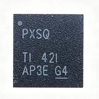
TPS7A7200RGWR - 2A, 6.5V Ultra-LDO with PG/EN | Texas Instruments
MPN: TPS7A7200RGWR ✓ NakahandaTPS7A7200RGWR Ulas
An LDO (Low-Dropout) linear regulator is a type of voltage regulator that maintains a stable output voltage even when the input voltage is very close to the output voltage, contrasting with switching regulators that use inductors and PWM control. LDOs belong to the linear regulator family, which sits under the voltage regulator hierarchy, which in turn belongs to the broader power management IC category. The TPS7A7200RGWR specifically targets high-current, low-voltage point-of-load (POL) conversion applications where a switching regulator's ripple would be unacceptable, trading efficiency for noise-free output and minimal BOM count.
Key differentiating features of the TPS7A7200RGWR include 180 mV dropout at 2 A (one of the lowest in its class), user-configurable output voltage from 0.9 V to 3.5 V without external feedback resistors (eliminating the error and drift these would introduce), integrated open-drain PG output for rail sequencing and fault monitoring, and active-high EN for on/off management. The device also features internal soft-start to limit inrush current, thermal shutdown, and current-limit protection. The VQFN-20 (RGW) package provides a low thermal resistance path that helps dissipate the heat generated when VIN-VOUT differential is large.
Technically, the TPS7A7200RGWR uses an internal P-channel pass element architecture (PMOS LDO), which is why its dropout is so low - PMOS LDO dropout is roughly RDS(on) x ILoad rather than Vth-limited like an NPN or N-channel LDO. The 0.9 V to 3.5 V output range is set via factory-configurable pin straps, meaning no external resistor divider is needed, and the output tolerance is tightened by avoiding external resistor drift over temperature.
Typical applications include powering FPGAs, DSPs, ASICs, and microcontrollers from 1.5 V, 1.8 V, 2.5 V, 3.3 V or 3.5 V rails, post-regulation after a switching DC-DC converter to clean up switching noise, and powering sensitive analog/RF blocks that demand low ripple. The fast transient response makes it ideal for digital loads with rapid current steps. When using this device, ensure the input-to-output voltage differential remains within SOA limits to avoid excessive power dissipation, especially at 2 A full load - use adequate copper pours on the exposed pad.
Mga alternatibo na pwedeng ilagay na TPS7A7200RGWR — parehas na package, pin-to-pin na katugmang. Hindi kasama ang mga bahagi ng iba't-ibang package na nangangailangan ng pagpapaayos ng PCB.
TPS7A7200RGWT
✅ Drop-In📋 Alternatibo na Reference (hindi sa katalogo)
TPS7A7100RGWR
✅ Drop-In📋 Alternatibo na Reference (hindi sa katalogo)
TPS7A8300ARGWR
✅ Drop-In📋 Alternatibo na Reference (hindi sa katalogo)
TPS7A7200RGTR
✅ Drop-In📋 Alternatibo na Reference (hindi sa katalogo)
TPS7A7200QRGWREP
✅ Drop-In📋 Alternatibo na Reference (hindi sa katalogo)
TPS7A7200RGWR Mga Pinakamataas na Rating at Electrical Characteristics
| Type ng Output | User-configurable, fixed (no external resistors) |
| Hanay ng Output Volte | 0.9 V to 3.5 V (factory set, pin-strap) |
| Maksimum na Current ng Output | 2 A |
| Hanay ng Voltage ng Input | 1.5 V to 6.5 V |
| Minimum VIN for Output Regulation | 1.43 V |
| Voltage ng Dropout | 180 mV at 2 A |
| Pin na Pinapayagan | Yes (active-high) |
| Output ng Power Dati | Yes (open-drain) |
| Load Transient Response | Very fast (per TI datasheet) |
| Hanay ng Temperature na Operasyon | -40C to +125C junction |
| Packhaging | VQFN-20 (RGW) 5x5 mm with exposed pad |
| Uri ng Pagpapasok | Surface Mount |
| Tindminan RoHS | Compliant |
| Pass Element | P-MOSFET (internal) |
Pin Configuration ng TPS7A7200RGWR
| Pin 1 | VIN — Input supply voltage (1.5 V to 6.5 V) |
| Pin 2 | VIN — Input supply voltage |
| Pin 3 | EN — Enable pin (active-high) |
| Pin 4 | PG — Power-good output (open-drain) |
| Pin 5 | VOUT — Regulated output voltage |
| Pin 6 | VOUT — Regulated output voltage |
| Pin 7 | VOUT — Regulated output voltage |
| Pin 8 | VOUT — Regulated output voltage |
| Pin 9 | VOUT — Regulated output voltage |
| Pin 10 | VOUT — Regulated output voltage |
| Pin 11 | VOUT — Regulated output voltage |
| Pin 12 | VOUT — Regulated output voltage |
| Pin 13 | VOUT — Regulated output voltage |
| Pin 14 | GND — Ground |
| Pin 15 | GND — Ground |
| Pin 16 | GND — Ground |
| Pin 17 | GND — Ground |
| Pin 18 | NC — Not connected (per datasheet) |
| Pin 19 | NC — Not connected (per datasheet) |
| Pin 20 | NC — Not connected (per datasheet) |
Tipikal na mga Gamit
TPS7A7200RGWR ay nararapat para sa 7 aplikasyons: FPGA/DSP Core Voltage Regulation, Post-Regulation After Switching DC-DC, ASIC/Microcontroller I/O and Auxiliary Rails, Single-Cell Li-Ion Powered Portable Devices, Industrial Sensor and Data Acquisition Systems, Networking and Communication Equipment, Test and Measurement Instrumentation.
FPGA/DSP Core Voltage Regulation
The TPS7A7200RGWR's 2 A output and 180 mV dropout make it ideal for powering FPGA and DSP core rails directly from a 3.3 V or 1.8 V system rail. The user-configurable 0.9 V to 3.5 V output range covers common core voltages (1.0 V, 1.2 V, 1.5 V, 1.8 V) without external resistors. The fast load-transient response handles the rapid current steps that FPGAs exhibit during logic-block switching, while the exposed thermal pad on the VQFN-20 package dissipates heat efficiently. Designers typically place the LDO between the upstream DC-DC converter and the FPGA VCORE pins, using 10 uF ceramic input/output capacitors for stability.
Inirekomenda
Post-Regulation After Switching DC-DC
After a switching buck regulator provides the bulk conversion, the TPS7A7200RGWR serves as a low-noise post-regulator to clean up switching ripple before sensitive analog/RF blocks. With only 180 mV dropout at 2 A and 1.43 V minimum VIN, it can regulate even when the upstream converter sags under load. The integrated power-good (PG) output allows sequencing coordination between the bulk regulator and the LDO. Place the TPS7A7200RGWR between the buck output and the analog AVDD pin with input/output ceramic capacitors.
Inirekomenda
ASIC/Microcontroller I/O and Auxiliary Rails
The TPS7A7200RGWR powers 1.8 V, 2.5 V, or 3.3 V I/O rails on ASICs and microcontrollers that draw up to 2 A peak current. The wide VIN range (1.5 V to 6.5 V) accepts either a 3.3 V main rail or a 5 V input directly, simplifying power tree design. The active-high EN pin allows MCU-controlled power-down for energy-saving states, while the PG output signals when the rail is in regulation. Use 22 uF ceramic output capacitors for optimal transient response with digital loads.
Inirekomenda
Single-Cell Li-Ion Powered Portable Devices
The TPS7A7200RGWR operates from a single-cell Li-ion battery (3.0 V to 4.2 V nominal) to produce 1.8 V or 2.5 V rails at 2 A for portable equipment, wearables, and battery-powered instruments. Its 1.43 V minimum VIN allows operation even as the battery discharges below 3 V, extending usable runtime. The low 180 mV dropout minimizes battery sag during high-current transients, and the small VQFN-20 (RGW) 5x5 mm footprint suits space-constrained PCB designs. Pair with battery management ICs for complete portable power solutions.
Inirekomenda
Industrial Sensor and Data Acquisition Systems
Industrial sensor systems requiring clean analog power benefit from the TPS7A7200RGWR's low-noise linear regulation at 2 A. The 1.5 V to 6.5 V VIN range accepts 3.3 V or 5 V industrial bus power directly, while the user-configurable 0.9 V to 3.5 V output covers common analog supply voltages. The -40C to +125C junction temperature rating supports industrial temperature grades. The PG output feeds fault monitoring circuits, and the exposed thermal pad manages heat in sealed industrial enclosures with limited airflow.
Inirekomenda
Networking and Communication Equipment
Networking line cards, routers, and switches use the TPS7A7200RGWR to provide clean 1.0 V, 1.2 V, or 1.5 V rails to network processors, SerDes PHYs, and switch ASICs. The 2 A capability handles burst current demands of packet processing, while the fast load-transient response prevents voltage excursions during sudden traffic loads. The PG output coordinates rail sequencing with adjacent regulators. Multiple TPS7A7200RGWR devices can be paralleled (with proper ballasting) for higher current requirements.
Inirekomenda
Test and Measurement Instrumentation
Bench-top and production test equipment uses the TPS7A7200RGWR to power DACs, ADCs, and precision measurement ICs with low-noise, high-current rails. The user-configurable output voltage supports multiple DUT voltage requirements without board modifications. The exposed thermal pad and wide operating temperature range support the thermal environment inside instrument enclosures. The EN pin enables automated test sequencing, while PG validates power integrity before measurements begin.
Inirekomenda
Buod ng mga Inirekomendang Produkto
Impormasyon ng Talumpati sa Engineering for TPS7A7200RGWR — ikabit, gabay sa disenyo, at impormasyon ng pagsunod sa kautusan.
Paunawang Hanapin
Ikabit sa Mga Alternatibo
| Parametro | Ito ang Producto | TPS7A7200RGWT | TPS7A7100RGWR | TPS7A8300ARGWR |
|---|---|---|---|---|
| Package | VQFN-20 (RGW) 5x5 mm | VQFN-20 (RGW) 5x5 mm - same | VQFN-20 (RGW) 5x5 mm - same | VQFN-20 (ARGW) 5x5 mm - same family |
| Brand | Texas Instruments | Texas Instruments | Texas Instruments | Texas Instruments |
| Enable Pin | Yes (active-high) | Yes (active-high) | Yes (active-high) | Yes (active-high) |
Pangunahing mga Pagkakaiba
- User-configurable output without external resistors (kumpara saGeneric adjustable LDO competitors)
- 180 mV dropout at 2 A full load (kumpara saStandard LDO competitors at 2 A)
- Integrated power-good (PG) and enable (EN) pins (kumpara saLower-cost 2 A LDOs without monitoring)
- Wide VIN range with 1.43 V minimum for regulation (kumpara saLDOs requiring VIN >= VOUT + 1 V headroom)
Talaan ng Disenyo
At VIN = 3.3 V, VOUT = 1.8 V, and 2 A load, estimated power dissipation is (3.3 - 1.8) x 2 = 3.0 W. Per the VQFN-20 (RGW) 5x5 mm package datasheet, the theta_JA is approximately 30-35 C/W on a standard JEDEC 4-layer test board, yielding a junction temperature rise of 90-105 C above ambient. For reliable operation at full 2 A load with non-trivial dropout, use generous copper pours on the exposed pad and consider thermal vias to inner ground planes. At 5 V VIN and 1.0 V VOUT at 2 A, dissipation rises to ~8 W - an external heatsink is recommended.
Per the TI TPS7A7200 datasheet layout guidelines, place the input capacitor (10 uF X7R ceramic minimum) as close as possible to the VIN pin and GND. The output capacitor (10 uF X7R minimum, 22 uF recommended for transient response) should be placed adjacent to the VOUT pin and GND. Use wide PCB traces or copper pours on VIN and VOUT to handle 2 A continuous current. Connect the exposed thermal pad to a large ground copper pour with multiple thermal vias for heat dissipation. Avoid routing sensitive analog signals near the LDO to prevent noise coupling.
Estimated: Do not exceed the absolute maximum VIN of 7 V (per datasheet) - leave at least 0.5 V margin. The TPS7A7200RGWR requires minimum load current for regulation; check the datasheet for the specific minimum load spec. Power-good (PG) output is open-drain and requires an external pull-up resistor (typically 10 kOhm to 100 kOhm) to VOUT or a logic rail. The EN pin has an internal pull-down; if left floating the device defaults to disabled - drive EN high to enable. Verify the factory-set output voltage option (0.9 V, 1.0 V, 1.2 V, 1.5 V, 1.8 V, 2.5 V, 3.3 V, 3.5 V) matches your application requirement when ordering.
Impormasyon ng Pagsunod sa Kautusan
RoHS compliant per TI product page. For AEC-Q100 automotive qualified version, choose TPS7A7200QRGWREP. Halogen-free status not explicitly stated in provided data.