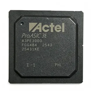
XC7A50T-1FG484C - 52K Artix-7 FPGA | AMD | Industrial Control
MPN: XC7A50T-1FG484C ✗ Tapus ng BuhayXC7A50T-1FG484C Ulas
What is an FPGA? A field-programmable gate array is a programmable digital semiconductor that combines configurable logic blocks, programmable interconnect, block RAM, and digital signal processing resources. An Artix-7 FPGA sits within the FPGA hierarchy: FPGA → Artix-7 → Xilinx 7-Series FPGA → programmable logic and embedded-processing platform. Unlike a fixed-function application-specific integrated circuit, an FPGA lets engineers define parallel hardware behavior through HDL, constraints, and device configuration.
The XC7A50T family is positioned for cost-sensitive systems that need more parallelism and I/O flexibility than a microcontroller or fixed interface device can provide. The verified distributor information specifically lists 250 I/Os and a 484-BBGA package, making the device relevant to industrial automation, data acquisition, communications, embedded control, and image or video processing systems. The 484-ball package supports dense board routing while providing a substantial external interface count.
The -1 speed designation, temperature suffix, and exact electrical limits are not fully specified in the supplied search excerpts. Consequently, operating temperature, I/O standards, core voltage, memory resources, clock-management resources, and power consumption must be confirmed against the AMD Artix-7 data sheet before schematic sign-off. Do not infer those specifications from the distributor title alone.
A practical design begins by partitioning the required datapath into parallel pipelines and selecting the smallest Artix-7 resource that satisfies timing, memory, DSP, and I/O constraints. The 250-I/O figure should be mapped against the board-level connector, transceiver, voltage-standard, and clock requirements. Pin assignment, bank voltage planning, configuration pins, decoupling, and power sequencing are more important than treating the FPGA as a generic high-pin-count component.
This page consolidates verified distributor identity and package information, separates known facts from missing technical data, and avoids fabricating alternatives or electrical ratings. Engineers should use the official AMD package files and datasheet for final pinout, timing, power, and migration decisions.
Mga alternatibo na pwedeng ilagay na XC7A50T-1FG484C — parehas na package, pin-to-pin na katugmang. Hindi kasama ang mga bahagi ng iba't-ibang package na nangangailangan ng pagpapaayos ng PCB.
Variante sa Seri na ito
Katulad na modelo sa serye na katugma sa pagpasok XC7A50T-1FG484C (parehas na form factor at footprint) — pagkakaiba sa Device Type, I/O Count, Logic Cells, Package Type.
XC7A50T-1FGG484C
✅ Drop-In📋 Alternatibo na Reference (hindi sa katalogo)
XC7A50T-1FGG484I
✅ Drop-In📋 Alternatibo na Reference (hindi sa katalogo)
XC7A50T-2FGG484C
✅ Drop-In📋 Alternatibo na Reference (hindi sa katalogo)
XC7A75T-1FGG484I
✅ Drop-InMagkontak para sa presyo
Tingnan ang Datasheet →XC7A50T-1FG484C-ND
✅ Drop-In📋 Alternatibo na Reference (hindi sa katalogo)
XC7A50T-1FG484C Mga Pinakamataas na Rating at Electrical Characteristics
| Device Type | Artix-7 field-programmable gate array (FPGA) |
| Manufacturer | AMD / Xilinx |
| Logic Cells | 52,000 cells |
| Verified Distributor Logic Value | 52,160 logic elements |
| I/O Count | 250 I/Os |
| Packhaging | 484-FBGA |
| Package Type | 484-ball BGA |
| Configuration Memory | 2,764,800 configuration bits |
| FPGA Family | Artix-7 |
| Programmability | User-programmable digital logic |
Gabay sa Pin Configuration ng XC7A50T-1FG484C 484-ball bga
Pin configuration para sa XC7A50T-1FG484C (484-ball bga package). Kasama sa digital IC na ito ang GPIO, mga communication interface (UART, SPI, I2C), at mga power pin. Sumangguni sa datasheet ng manufacturer para sa mga alternatibong function ng pin at mga opsyon sa configuration. Mahalaga para sa disenyo ng embedded system at PCB layout.

Wala ng detalyadong pinout data na magagamit para sa XC7A50T-1FG484C.
Sumangguni sa datasheet para sa buong pin configuration.
Tipikal na mga Gamit
XC7A50T-1FG484C ay nararapat para sa 6 aplikasyons: Industrial Automation and PLC Control, Data Acquisition and Signal Conditioning, Communications Interface Bridging, Video and Image Processing, Motor Control and Real-Time Systems, Embedded Instrumentation and Test Equipment.
Industrial Automation and PLC Control
The AMD XC7A50T-1FG484C is a strong fit for industrial automation when a controller needs deterministic parallel logic and broad external connectivity. Its verified 52,160 logic elements provide substantial programmable capacity, while the listed 250 I/Os can serve digital sensors, actuator outputs, encoders, interlock signals, and communications transceivers. The FPGA can implement multiple parallel control loops or timing channels without relying entirely on a microcontroller. Before schematic release, verify the exact I/O voltage standards, bank limitations, clocking resources, and power requirements in the AMD Artix-7 documentation. The -1 speed code and C temperature suffix must also be checked against the system’s timing and environmental requirements.
Inirekomenda
Data Acquisition and Signal Conditioning
XC7A50T-1FG484C can support parallel data-acquisition front ends because programmable logic allows sampling, filtering, decimation, and buffering to be organized as dedicated hardware pipelines. The verified 250-I/O count is useful when multiple channels must be captured or routed concurrently, although the supplied data does not specify maximum I/O rates or supported voltage standards. Engineers should use the AMD pinout and timing resources to map analog front-end control signals, ADC interfaces, clocks, and trigger lines. A practical design keeps high-speed routing short, defines timing constraints for every external interface, and verifies power sequencing and bank compatibility before layout release.
Inirekomenda
Communications Interface Bridging
The XC7A50T-1FG484C is suitable for communications interface bridging, protocol conversion, and packet pre-processing when multiple lanes or parallel bus signals must be handled in hardware. Its programmable logic capacity supports state machines, FIFOs, clock-domain crossing, and fixed-format data routing, while 250 listed I/Os provide many external connections. The verified data does not specify transceiver resources, maximum lane rates, or supported standards, so engineers must consult the exact AMD family data sheet and package files. A successful implementation should define clock domains early, constrain all interfaces, and check whether the selected board-level transceiver—not merely the FPGA I/O count—sets the achievable data rate.
Inirekomenda
Video and Image Processing
The XC7A50T-1FG484C can be evaluated for image and video pipelines because it offers approximately 52,000 logic elements and a large listed I/O count for parallel or serialized interface circuitry. Programmable logic can implement pixel formatting, filtering, color conversion, line buffers, and control sequencing, but the supplied evidence does not state block RAM, DSP, or video-interface resources. Those missing parameters must be verified before making a throughput claim. Engineers should calculate storage bandwidth, clock requirements, frame latency, and I/O lane count, then run AMD synthesis and timing analysis with realistic constraints. The 484-FBGA package also demands careful ball assignment and signal-integrity planning.
Inirekomenda
Motor Control and Real-Time Systems
XC7A50T-1FG484C is relevant to motor-control and real-time embedded systems because FPGA logic can execute parallel current-control, position, PWM, and fault-detection functions with predictable hardware behavior. The verified device provides 52,160 logic elements and 250 I/Os, leaving room for control-law pipelines and external gate-driver or position-sensor interfaces. The supplied data does not state internal clocking, memory, or timing details, so the design team should calculate worst-case clock and I/O constraints and verify the exact speed grade. Use synchronous clocking, isolated power domains, and defined shutdown paths for motor systems, and validate thermal performance against the actual utilization estimate.
Inirekomenda
Embedded Instrumentation and Test Equipment
The XC7A50T-1FG484C can be used in programmable instrumentation when flexible sequencing, parallel data capture, and deterministic control are more valuable than a fixed application-specific device. Verified resources of 52,160 logic elements and 250 I/Os can support control logic, pattern generation, trigger conditioning, and status reporting. The supplied results do not specify analog blocks, DAC resources, or maximum clock rates, so the part should be selected against the complete AMD device tables rather than marketing descriptions alone. For laboratory equipment, define safe control defaults, implement configuration monitoring, and verify that the selected package has adequate escape routing for test connectors and high-speed clocks.
Inirekomenda
Buod ng mga Inirekomendang Produkto
Impormasyon ng Talumpati sa Engineering for XC7A50T-1FG484C — ikabit, gabay sa disenyo, at impormasyon ng pagsunod sa kautusan.
Paunawang Hanapin
Ikabit sa Mga Alternatibo
| Parametro | Ito ang Producto | XC7A50T-1FGG484C | XC7A50T-1FGG484I | XC7A50T-2FGG484C | XC7A75T-1FGG484I | XC7A50T-1FG484C-ND |
|---|---|---|---|---|---|---|
| Package | 484-FBGA | 484-FBGA | 484-FBGA | 484-FBGA | 484-FBGA | 484-FBGA |
| Brand | AMD / Xilinx | AMD / Xilinx | AMD / Xilinx | AMD / Xilinx | AMD / Xilinx | AMD / Xilinx |
| FPGA Family | Artix-7 | Artix-7 | Artix-7 | Artix-7 | Artix-7 | Artix-7 |
| Speed Suffix | -1 | -1 | -1 | -2 | -1 | -1 |
| Temperature Suffix | C | C | I | C | I | ND |
Pangunahing mga Pagkakaiba
- Verified 52,160-element Artix-7 configuration target (kumpara saXC7A75T-1FGG484I)
- Commercial C suffix alignment (kumpara saXC7A50T-1FGG484I)
- Direct -1 speed-suffix family positioning (kumpara saXC7A50T-2FGG484C)
- Large listed connectivity (kumpara saXC7A50T-1FGG484C)
Talaan ng Disenyo
Treat the 484-FBGA as a high-density routed package rather than a generic through-hole footprint. Assign power, ground, configuration, clock, and high-speed interface balls from the exact AMD package files, keep BGA escape routing within the manufacturer’s supported stack-up assumptions, and confirm that the PCB fabricator supports the selected ball pitch and via structure. Do not infer missing pin functions from the distributor package name.
Plan the power tree from the official Artix-7 power-supply requirements before placing decoupling. Separate core, auxiliary, and I/O supplies according to the exact device data sheet, verify permitted sequencing, and reserve local high-frequency and bulk capacitance at the package. The supplied evidence gives no voltage or power values, so estimates must be labeled as estimates and replaced with verified datasheet values before schematic release.
Constrain every external interface at the actual board-level rate, not only the FPGA fabric clock. Define input and output delays for clocks, data buses, and reset signals; keep clock routes short and controlled; and reserve return-path continuity through the BGA escape network. Run post-route timing and signal-integrity checks against the exact package and board stack-up because the provided results contain no I/O timing or impedance data.
Do not treat XC7A50T-1FGG484C, XC7A50T-1FGG484I, or XC7A50T-1FG484C-ND as guaranteed substitutes merely because the ordering codes resemble XC7A50T-1FG484C. Verify package pin files, speed grade, temperature range, configuration interface, lifecycle terms, and timing constraints. For a migration, compare utilization and timing results rather than relying on the family name alone.
Impormasyon ng Pagsunod sa Kautusan
Compliance information was not included in the verified search excerpts. RoHS, REACH, lead-free, halogen-free, conflict-minerals, and automotive qualification must be confirmed from the exact AMD product documentation or supplier declaration.