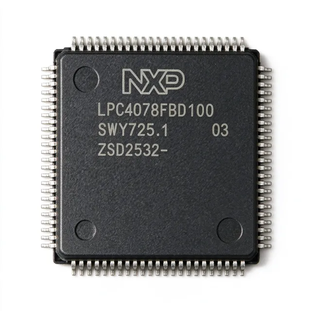
What Is the LPC4078FBD100 and Is It Currently Available?
The LPC4078FBD100 is a 32-bit ARM Cortex-M4 microcontroller from NXP Semiconductors with a single-precision FPU, a maximum clock frequency of 120 MHz, 512 KB of on-chip flash, and 96 KB of SRAM. It is supplied in a surface-mount 100-LQFP package measuring 14 mm by 14 mm and operates from 2.4 V to 3.6 V over -40°C to +85°C. Current XAIPART inventory data shows 26,000 units, while the component is in last-time-buy status. Its verified pricing ranges from $12.6563 at one unit to $7.3828 at 1,000 units, as of 2026-11-01. Buyers should qualify a successor before committing new production demand.
Beyond the core and memory, the device integrates three I2C interfaces, including one Fast-mode Plus interface supporting 1 Mbit/s; one 12-bit, 8-channel ADC; one 10-bit DAC; two analog comparators; an I2S interface; and USB Host, Device, and OTG support. Its peripheral highlights also include Ethernet MAC, CAN, an SD card interface, and an LCD controller. This combination places the LPC4078FBD100 between general-purpose microcontroller control and higher-integration embedded DSP work.
| Verified parameter | Value |
|---|---|
| Core | ARM Cortex-M4 |
| Architecture | 32-bit RISC with single-precision FPU |
| Maximum clock frequency | 120 MHz |
| Program memory | 512 KB Flash |
| SRAM | 96 KB |
| Package | 100-LQFP (14 mm × 14 mm) |
| Mounting type | Surface Mount |
| Supply voltage | 2.4 V to 3.6 V |
| Operating temperature | -40°C to +85°C (industrial) |
| ADC | 1 × 12-bit, 8-channel |
| DAC | 1 × 10-bit |
| I2C interfaces | 3; one Fast-mode Plus at 1 Mbit/s |
| I2S interface | Yes; digital audio input/output |
| Analog comparators | 2 |
| RoHS status | Compliant |
| Lead-free | Yes |
Use the LPC4078FBD100 product page to review the current offer, and consult the official NXP LPC407x/8x datasheet before starting a board revision or a migration.
Takeaway: The LPC4078FBD100 remains purchasable with 26,000 units shown in stock, but its last-time-buy status makes successor qualification a prerequisite for every new production program.
How Do You Design In the LPC4078FBD100?
Start with the fixed resources the product provides: a 120 MHz Cortex-M4 core, 512 KB of flash, 96 KB of SRAM, and a 2.4 V to 3.6 V operating range. The 8.33 ns clock period at 120 MHz gives designers a straightforward timing basis for control loops and peripheral service routines. Use the single-precision FPU for floating-point control calculations and the Cortex-M4 DSP capabilities for signal-processing work. The verified 96 KB SRAM should be treated as the primary working-memory budget because the part has 512 KB of flash for program storage rather than general data storage.
The 100-LQFP pinout exposes enough parallel I/O to connect multiple mixed-signal and communications functions without immediately adding a companion controller. Relevant functions include I2C, I2S, USB, Ethernet, CAN, ADC inputs, a DAC output, LCD signals, and dedicated 3.3 V power pins. Pin multiplexing means the final board design must assign each required peripheral to a specific pin and verify that no two functions occupy the same package ball. The key package pins are available in the structured pinout data below; the complete assignment remains on the product page.
| Design area | Verified resource | Engineering action |
|---|---|---|
| Core and timing | 120 MHz ARM Cortex-M4 with single-precision FPU | Use an 8.33 ns clock period as the device-rate reference and validate control-loop latency in firmware. |
| Firmware storage | 512 KB Flash | Reserve code space for the selected protocol stack, bootloader, diagnostics, and application firmware. |
| Working memory | 96 KB SRAM | Budget buffers and stack usage before enabling multiple communication protocols. |
| Power | 2.4 V to 3.6 V | Design the rail within the verified operating range and account for all connected loads. |
| Decoupling | 100 nF ceramic capacitor near every VDD/VSS pair | Follow the NXP LPC407x reference schematic and user manual during layout. |
| Analog conversion | 1 × 12-bit, 8-channel ADC; 1 × 10-bit DAC | Map sensor inputs and the analog output to their multiplexed package pins. |
| Digital audio | I2S digital audio input/output | Assign I2S clock, word-select, and data pins without conflicting with other peripheral functions. |
| Local connectivity | Three I2C interfaces; one supports 1 Mbit/s | Place the faster bus on correctly routed signals and keep its rate within the verified interface capability. |
| USB | Host, Device, and OTG | Reserve USB data, VBUS sense, and soft-connect functions in the pin plan. |
| Ethernet | Ethernet MAC | Use the dedicated Ethernet pin group and the NXP reference design for the external interface implementation. |
Power layout deserves particular attention. The verified pinout identifies VDD and VSS locations at pins 11/12, 37/38, 69/70, and 85/86. Place the specified 100 nF ceramic capacitors close to the relevant VDD/VSS pairs and follow the NXP LPC407x user manual and reference schematic. This step is not optional if the design depends on the advertised 120 MHz operation or sensitive analog conversion.
For migration, NXP documents pin-function compatibility with the LPC23xx/24xx and LPC178x/7x families. That compatibility can reduce board rework, but it does not remove the need for firmware recompilation and peripheral-mapping review. Check the latest errata sheet, boot configuration, clock setup, pin multiplexing, and power sequencing before declaring a board drop-in compatible.
The XAIPART engineering blog provides supporting material for broader embedded-design decisions, while the CuprumFlow graphics article offers context for human-machine-interface design considerations.
Takeaway: A successful design starts with a pin-by-pin peripheral allocation, verified power and decoupling layout, and an explicit migration review; package similarity alone does not validate a drop-in upgrade.
Which Alternatives Can Replace the LPC4078FBD100?
The LPC4088FBD100 is the direct capacity-oriented alternative because it retains the 120 MHz Cortex-M4 core, the same peripherals, and the same 100-LQFP package while increasing flash from 512 KB to 1 MB. It is the appropriate candidate when firmware growth makes the original 512 KB insufficient. The LPC4076FBD100 provides 256 KB of flash and the LPC4074FBD100 provides 128 KB while retaining the same core and peripherals, making them lower-memory options rather than equivalent substitutes for a firmware image that exceeds their capacity.
Two suffix variants, LPC4078FBD100K and LPC4078FBD100E, use the same die as the LPC4078FBD100 and are identified as packing or variant parts with pin-to-pin compatibility. Their procurement status, temperature coverage, and availability must be checked separately before using either as a production substitute. “Pin-to-pin compatible” addresses the physical package and pin arrangement; it does not by itself prove equivalent lifecycle terms, distributor stock, or delivery availability.
| Parameter | LPC4078FBD100 | LPC4078FBD100K | LPC4078FBD100E | LPC4076FBD100 | LPC4074FBD100 | LPC4088FBD100 |
|---|---|---|---|---|---|---|
| Core | ARM Cortex-M4 | Same die as LPC4078FBD100 | Same die as LPC4078FBD100 | ARM Cortex-M4 | ARM Cortex-M4 | ARM Cortex-M4 |
| Maximum clock | 120 MHz | 120 MHz | 120 MHz | 120 MHz | 120 MHz | 120 MHz |
| Flash | 512 KB | 512 KB | 512 KB | 256 KB | 128 KB | 1 MB |
| Flash change versus LPC4078FBD100 | Baseline | No change | No change | -50% | -75% | +100% |
| Package | 100-LQFP | Same 100-LQFP package | Same 100-LQFP package | Same 100-LQFP package | Same 100-LQFP package | Same 100-LQFP package |
| Pin compatibility | Reference part | Pin-to-pin compatible | Pin-to-pin compatible | Pin-to-pin compatible | Pin-to-pin compatible | Pin-to-pin compatible |
| Peripheral set | Reference set | Same die and pin compatibility | Same die and pin compatibility | Same core and peripherals | Same core and peripherals | Same core and peripherals |
| SRAM | 96 KB | Not separately stated | Not separately stated | Not separately stated | Not separately stated | Not separately stated |
Selection should follow three checks. First, confirm that the firmware and update strategy fit the available flash. Second, confirm the 96 KB SRAM requirement where the alternative’s SRAM is not separately stated. Third, verify lifecycle status, stock, date codes, and ordering terms for the exact suffix. The XAIPART component catalog should be used to check the exact MPN rather than assuming that every suffix has the same commercial position.
Do not treat an STM32F407VGT6 or any other device from a different vendor as a drop-in replacement for this LPC4078FBD100. The supplied comparison set is limited to LPC407x and LPC408x devices with verified pin compatibility, so cross-vendor selections require a separate board, firmware, and peripheral-mapping review.
Takeaway: Choose LPC4088FBD100 for additional flash, LPC4076FBD100 or LPC4074FBD100 only when the reduced code space is acceptable, and treat the K and E suffix variants as sourcing options requiring separate commercial verification.
What Does Its Lifecycle and Supply Status Mean for Buyers?
The LPC4078FBD100 is in last-time-buy status. That status changes the procurement objective: the available inventory can support existing demand, but it should not be treated as a repeatable new-production supply line. XAIPART shows 26,000 units of stock and pricing across nine distribution channels. The volume pricing structure falls from $12.6563 at quantities of one or more to $9.1406 at 10, $8.0859 at 100, $7.7344 at 500, and $7.3828 at 1,000 units, as of 2026-11-01.
| Quantity threshold | Verified unit price | Pricing date |
|---|---|---|
| 1 or more | $12.6563 | As of 2026-11-01 |
| 10 or more | $9.1406 | As of 2026-11-01 |
| 100 or more | $8.0859 | As of 2026-11-01 |
| 500 or more | $7.7344 | As of 2026-11-01 |
| 1,000 or more | $7.3828 | As of 2026-11-01 |
Buyers should separate the component’s physical availability from its long-term availability. A stock quantity can support a near-term build, but last-time-buy status signals that replenishment is not assured. Existing programs should obtain a firm quotation, confirm date codes, and place replenishment orders before the available inventory becomes constrained. New programs should compare the LPC4088FBD100 and other qualified LPC407x/8x options rather than designing a permanent new product around a last-time-buy part.
The verified $7.3828 base price aligns with the verified 1,000-unit pricing tier. Earlier narrative pricing should not override the current tier data. Any quoted broker, obsolete, or nonstandard-market price should be evaluated separately rather than blended into the authorized-channel price ladder.
Available application directions include industrial automation controllers, building-automation HMI panels, point-of-sale terminals, motor-control and BLDC drives, audio recording and playback peripherals, and legacy LPC23xx/24xx migration designs. This breadth can affect how quickly inventory disappears, particularly when an existing design requires a qualified same-package successor. Confirm the exact final buy window and delivery schedule directly with NXP or an authorized distributor.
Takeaway: Use the current stock for a controlled buy of existing demand, but qualify a successor now; last-time-buy inventory supports continuity only until that inventory and the final-order window are exhausted.
What Should Buyers Watch in Future Designs?
The first design watchpoint is memory headroom. The LPC4078FBD100 provides 512 KB of flash and 96 KB of SRAM, while the verified LPC4088FBD100 alternative doubles flash to 1 MB without changing the core speed or package. For long-lived industrial, HMI, motor-control, or networked products, a 1 MB code budget can reduce the risk of a late redesign when diagnostics, communications, or control features expand. The actual firmware-image size must determine the choice; the larger part is valuable only when the additional memory is needed.
The second watchpoint is mixed-signal and communications integration. The combination of an 8-channel 12-bit ADC, 10-bit DAC, two analog comparators, three I2C interfaces, I2S, USB, Ethernet MAC, CAN, SD, and an LCD controller can eliminate several discrete support devices. That integration makes board planning more demanding because these functions share a fixed set of multiplexed pins. As designs add I2S audio, USB connectivity, Ethernet, and LCD control simultaneously, validate the pin assignment and signal routing before schematic release.
The third watchpoint is the combination of high core rate and constrained code capacity. At 120 MHz, the Cortex-M4 core provides 25 million core clock cycles per second. The 1 MB LPC4088 option provides twice the flash of the 512 KB base part, which can be useful when control code, communications stacks, and field-upgrade logic must coexist. Developers should therefore compare both clock rate and memory rather than treating the higher-frequency alternative as a substitute without checking software requirements.
The fourth watchpoint is lifecycle stability. The last-time-buy status makes component continuity more important than headline processor performance. For new industrial programs, specify the selected successor, confirm its supply status, and establish a controlled migration plan before the installed base becomes large enough to make changes expensive. For existing designs, monitor remaining stock and obtain a final-buy quotation. A broader view of embedded development practices is available through the ESP-Mosaico AI coding article.
The final watchpoint is validation rather than headline matching. A drop-in claim is useful for package and pin planning, but the design still requires review of boot configuration, peripheral multiplexing, clock initialization, power sequencing, decoupling, and errata. For legacy LPC23xx/24xx and LPC178x/7x migrations, recompile the firmware and verify every reused peripheral assignment even when the board footprint remains unchanged.
| Buyer watchpoint | Verified basis | Action |
|---|---|---|
| Program-memory headroom | 512 KB versus 1 MB in LPC4088FBD100 | Measure the final firmware image and reserve upgrade space. |
| Working-memory budget | 96 KB SRAM in LPC4078FBD100 | Include stack, communication buffers, and application data in the memory budget. |
| Pin multiplexing | I2C, I2S, USB, Ethernet, CAN, LCD, ADC, and DAC functions share the 100-LQFP device | Complete a package-level pin matrix before PCB layout. |
| Lifecycle continuity | Last-time-buy status and 26,000 units of stock | Qualify a successor and place a controlled buy for existing demand. |
| Power integrity | 2.4 V to 3.6 V supply; 100 nF ceramic decoupling at VDD/VSS pairs | Follow the NXP reference schematic and user manual. |
| Temperature requirements | -40°C to +85°C operating range | Confirm that the full product environment stays within the verified range. |
Takeaway: Future-proofing this design means balancing firmware and SRAM against the 512 KB baseline, protecting pin and power-plan integrity, and selecting a lifecycle-qualified successor before last-time-buy supply constrains the schedule.
Yorumlar
İlk yorumu yapın.
🔐 Lütfen giriş yap bir yorum göndermek için.
Hesabınız yok mu? Kayıt ol