Yükselteç IC'leri
Ürünler (1.100+)

LM359M - Dual 400 MHz Norton Amplifier | Texas Instruments
The Texas Instruments LM359M is a dual, high-speed, programmable current-mode Norton amplifier with two independent amplifier circuits, a 400 MHz gain-bandwidth product, and a 60 V/µs slew rate. The LM359M is supplied in a 14-SOIC package and is intended for applications requiring high-frequency operation, user-programmable gain, and flexible feedback arrangements. An operational amplifier is an active analog signal-conditioning device that amplifies the difference between two input voltages while using negative feedback to set closed-loop behavior. The LM359 uses a current-mode, or Norton, input architecture rather than the voltage-input architecture common in conventional voltage-feedback amplifiers. This topology can provide high speed and high gain-bandwidth performance when supported by suitable external current-setting and compensation networks. The LM359 family provides two amplifiers in one package, reducing component count in dual-channel signal paths. Its high gain-bandwidth product makes it useful in video, communications, instrumentation, and active-filter circuits where signal bandwidth matters. The user-programmable gain and frequency characteristics allow circuit designers to tailor amplifier behavior with external resistors and capacitors, although stability must be checked for each selected feedback network. The LM359M is a 14-SOIC device with two amplifier sections, separate supply pins, and exposed package leads for through-hole board assembly or compatible PCB land patterns. Because it is a current-mode amplifier, input bias current, feedback-current selection, compensation, and maximum output swing require attention during design. The 400 MHz gain-bandwidth product does not mean every closed-loop circuit will operate at 400 MHz; usable bandwidth depends on gain, noise, stability, loading, and the external network. Typical uses include wideband video signal conditioning, pulse shaping, communications interfaces, active filters, oscillators, and instrumentation. The device is also suitable for educational and laboratory designs where a programmable high-speed analog amplifier is useful. Designers should begin with the manufacturer LM359 datasheet and verify the recommended external components for the intended gain and frequency response. A key design consideration is that LM359M is not a universal replacement for every voltage-feedback operational amplifier. Feedback topology, input bias-current behavior, compensation, output drive, and supply requirements must be checked against the original circuit. Stable operation also requires careful PCB layout, short feedback paths, suitable bypassing, and controlled parasitic capacitance. This page combines verified manufacturer and distributor information, package and application context, practical design guidance, and clearly identified data gaps. It is intended to help engineers evaluate LM359M for high-speed dual-amplifier designs without confusing its current-mode architecture with conventional voltage-feedback amplifier families.
LM359M/NOPB - Dual 400MHz High-Speed Amplifier | TI
Texas Instruments LM359M/NOPB is a dual, high-speed, programmable current-mode Norton operational amplifier with a 400 MHz gain-bandwidth product, 60 V/µs slew rate, 8 µA input bias current, and 40 mA output current per channel, packaged in a 14-SOIC tube package. The part is designed for high-frequency signal-chain work where user-programmable operating characteristics and stable inverting operation are important. The LM359 is an operational amplifier, a voltage-feedback signal-conditioning building block that compares an input signal with a feedback network and produces an amplified output. Its current-mode architecture places emphasis on high-frequency performance rather than the conventional high-impedance voltage-mode input used by many general-purpose amplifiers. The LM359 family therefore belongs to the broader category of analog ICs, operational amplifiers, and high-speed active signal-conditioning devices. Key features include two amplifier circuits on one monolithic IC, a 400 MHz gain-bandwidth product, 60 V/µs slew rate, and programmable amplifier operating characteristics. Each channel is broadbanded for high-frequency use, and the manufacturer identifies stable operation for inverting closed-loop gains of 10 or greater. The verified source data also lists 8 µA input bias current and 40 mA output current per channel, making the device suitable for analog signal conditioning, pulse processing, communications, and general-purpose amplification. The LM359M/NOPB ordering suffix identifies a specific Texas Instruments package and delivery configuration. The verified distributor data identifies the device as a dual general-purpose amplifier in a 14-SOIC case, while the target MPN is supplied in tube packaging. The NOPB designation is retained exactly as requested; package, temperature, and qualification details not explicitly present in the supplied data are marked as needed rather than inferred. Typical applications include high-frequency analog signal conditioning, communications interfaces, waveform shaping, pulse amplification, active filtering, and industrial or consumer control systems. Designers should preserve the recommended feedback and gain configuration, provide adequate bypassing, and verify stability experimentally because the current-mode Norton architecture and its programmable characteristics are not interchangeable with ordinary voltage-mode amplifier layouts without validation. For a new design, first confirm the required gain, bandwidth, output loading, supply arrangement, and package footprint against the manufacturer datasheet. Keep high-speed feedback traces short, place compensation and bypass components close to the relevant pins, and compare measured gain, phase margin, output swing, and slew behavior in the final board environment. This page synthesizes the verified manufacturer and distributor information with practical design guidance rather than claiming an unpublished full electrical table. Because the supplied web results do not include complete verified pin assignments, electrical limits, compliance declarations, or a reliable set of pin-compatible substitutes, those fields remain explicitly identified as data-needed. The most defensible purchasing and replacement decision requires checking the current Texas Instruments datasheet and distributor cross-reference results before production release.
LM359MX - Dual 60V/us High-Speed Amplifier | Texas Instruments
The Texas Instruments LM359MX is a dual, high-speed, programmable current-mode Norton amplifier with a 60 V/us slew rate, supplied in a 14-SOIC package. Each channel provides independent input-offset balancing, gain programming, frequency compensation, and output saturation control. The verified listing identifies two general-purpose amplifier circuits in one package, making LM359MX suitable for analog signal conditioning, waveform shaping, and programmable-gain systems. A current-mode amplifier, commonly called a Norton amplifier, senses input current rather than directly measuring input voltage. LM359MX uses that architecture to achieve high bandwidth and fast slew performance while allowing gain and compensation to be programmed with external components. Each amplifier can therefore adapt its dynamic behavior to a particular signal bandwidth, gain, or output-drive requirement rather than operating only with fixed internal settings. The two independent channels support simultaneous analog processing or separate signal paths. Programmable operating characteristics are useful when one circuit must amplify small instrumentation signals and another must process faster pulses. The 60 V/us slew rate helps preserve large-signal waveform fidelity, while the dual configuration can reduce component count where two compatible amplifier functions are needed. Typical uses include pulse and transient amplifiers, analog summing stages, video or communications interface signal conditioning, laboratory interfaces, and wideband control loops. Because operating characteristics are programmable, the external network around each channel is as important as the nominal device specifications. Feedback components, compensation values, source impedance, and output loading must be selected together to maintain intended bandwidth and stability. For PCB layout, use a grounded return path near each amplifier, keep sensitive input and feedback traces short, and place compensation components close to their associated pins. The tape-and-reel ordering suffix MX identifies the verified LM359MX package configuration, while the functional LM359 family documentation describes the shared dual current-differencing architecture and programmable operating behavior. This page combines the verified manufacturer and distributor listing data with engineering guidance for the LM359MX. It also makes missing electrical limits and availability values explicit rather than inferring them, allowing designers to evaluate the device against the full LM359 datasheet and current authorized-distributor inventory before releasing a design.

LM359N/NOPB - Dual 400MHz Norton Op-Amp, 14-DIP | Texas Instruments
The Texas Instruments LM359N/NOPB is a dual, high-speed, programmable, current-mode (Norton) amplifier integrated circuit housed in a 14-pin PDIP through-hole package. Each of the two independent amplifiers delivers a 400 MHz gain bandwidth product and a 60 V/µs slew rate, while providing user-programmable operating current and bandwidth through external resistors. The device operates from standard ±5V to ±15V (or single-supply 10V to 30V) supplies and is specified across the commercial 0 °C to +70 °C temperature range, making it suitable for cost-sensitive broadband and high-frequency signal-conditioning applications. A Norton (current-differencing) amplifier is a class of operational amplifier whose inverting input senses current rather than voltage, derived from classic current-differencing telemetry circuits. In the broader signal-chain hierarchy, Norton amplifiers belong to the linear IC family, sit alongside conventional voltage-feedback op-amps, and are commonly used as front-end gain blocks, video buffers, oscillators, comparators, and high-frequency AC amplifiers where standard op-amps lack sufficient speed. The LM359N/NOPB's two independent channels let one IC implement a complete two-stage function such as cascaded video gain or quadrature oscillator channels. Key features include a 400 MHz gain-bandwidth product, 60 V/µs slew rate, two independent Norton input stages, externally programmable quiescent current and bandwidth, and stable operation at closed-loop inverting gains of 10 or greater. Each amplifier can be biased to trade bandwidth against supply current, allowing designers to optimize power consumption for the target signal frequency. The 14-PDIP through-hole footprint simplifies prototyping, breadboarding, and legacy repair work on industrial control cards. The LM359 architecture pairs a current differencing input with a high-gain voltage output stage, yielding good high-frequency response that approaches that of much more expensive RF amplifiers. Because each amplifier's operating current is set by a single external resistor, the same device can serve as a 400 MHz wideband buffer or be reconfigured as a lower-power 50 MHz block by simply increasing the programming resistor. This flexibility is a key reason the part remains popular in instrumentation, video, RF, and oscillator designs decades after introduction. Typical applications include video and pulse amplifiers, RF and IF signal conditioning, wideband oscillators, current-mode comparators, and high-speed integrators. The two-amplifier configuration also suits active filter designs and instrumentation front ends that need matched channels. Designers retrofitting older equipment will find the DIP package convenient when working with through-hole production lines and replacement sockets. When designing with the LM359N/NOPB, program each amplifier's bandwidth and supply current through the I_set pin to balance power dissipation against required slew rate. A small ceramic bypass capacitor close to the supply pins is recommended to maintain high-frequency PSRR, and PCB traces to the inverting input should be kept short to minimize stray capacitance that could destabilize the high-gain stages.

LM3886TF - 68W Mono Class-AB Audio Amplifier w/ Mute | Texas Instruments
The Texas Instruments LM3886TF is a high-performance 68W continuous-average mono audio power amplifier with mute, housed in an 11-pin TO-220-11 Isolated (KC) through-hole package with an isolated tab. Operating from a single supply of 20V to 94V (or split ±10V to ±47V), the LM3886TF delivers 68W into 4Ω and 38W into 8Ω at 0.1% THD+N across the 20Hz–20kHz audio band, while the Class-AB topology preserves the low crossover distortion audiophile-grade designers expect from the Overture series. The device also includes a dedicated mute pin, SPiKe protection (short-circuit, thermal, over-voltage, under-voltage), and self-peak instantaneous temperature (°C) limiting. A Class-AB audio power amplifier is a linear amplifier topology that biases the output stage with a small quiescent current so both transistors conduct at the zero-crossing point, eliminating the crossover distortion of pure Class-B designs while still achieving high efficiency. Within the broader signal-chain taxonomy, the LM3886TF sits as a power-output stage downstream of a pre-amplifier and DAC/ADC, and belongs to the audio amplifier IC family, itself a sub-category of amplifier ICs (signal conditioning > amplifiers > audio amplifiers > power amplifier ICs). The Overture — LM3886 — series is TI's flagship monolithic hi-fi amplifier line. Key features of the LM3886TF include 0.1% THD+N at full output, 92dB minimum signal-to-noise ratio, 4Ω to 8Ω stable load drive, internal gain of 26dB (user adjustable with two external resistors), and a wide 20V–C to +85C excursion for the mute pin. The TO-220-11 isolated package provides 170°C/W maximum power dissipation. The Overture series signal-to-noise ratio minimum is a key differentiator over competing monolithic audio ICs. Typical applications include high-power mono subwoofer amplifiers, studio reference monitors, professional PA amplifiers, guitar combo amplifiers, and integrated stereo amplifiers (one LM3886TF per channel). The mute control pin allows use with a microcontroller or DSP interface to enable sequential power-up and standby control. When designing with the LM3886TF, ensure adequate heat-sinking—the isolated tab simplifies mounting on a chassis-coupled heat sink without requiring an insulating thermal pad (though one is optional). Use a low-impedance ground return, place the input RC network close to the pins, and observe the 94V absolute-maximum supply to avoid SPiKe protection tripping. The mute pin must be either driven high (>90%) or pulled low (<10% static) for proper operation—do not leave it floating or noise above 90 dB SNR will be compromised.

LM3886TF/NOPB - 68W Class-AB Audio Power Amplifier | TI
The Texas Instruments LM3886TF/NOPB is a high-performance 68W mono Class-AB audio power amplifier with mute, housed in an 11-pin TO-220 (NDA) isolated package. The device delivers 68W continuous average power into a 4 ohm load and 38W into 8 ohm with 0.1% THD+N across the 20 Hz to 20 kHz audio band, from a single supply of 20V to 94V. The TF suffix denotes a fully-isolated TO-220 leadform, while the NOPB suffix indicates lead-free / RoHS compliance. An audio power amplifier is the final analog stage that converts a low-level line-level input into a high-current, low-impedance signal capable of driving a loudspeaker. Class-AB topology blends the low conduction losses of Class-B with the low crossover distortion of Class-A, giving a compromise of efficiency and linearity that has dominated hi-fi amplifier design for decades. The LM3886 sits in the broader power management and amplifier IC hierarchy: audio amplifier -> Class-AB amplifier -> linear power amplifier -> analog output stage. Its self-peak instantaneous temperature (SPiKe) protection is a hallmark of the Overture series. Key specifications include 92 dB minimum open-loop gain, 0.03% typical THD+N at 1 kHz into 4 ohm, a slew rate of 19 V/us typical, and an operating temperature range of 0C to +70C. The mute function is logic-level controlled and the device includes internal current limiting and thermal shutdown. The fully-isolated TO-220 package permits direct mounting to a heatsink without an additional insulator pad, simplifying mechanical assembly. The bipolar output stage uses TI's SPiKe protection circuit, which provides dynamic, cycle-by-cycle current limiting as well as thermal shutdown. This yields a robust amplifier that tolerates output short circuits, reactive loads, and thermal overloads without destructive failure, making the LM3886 a long-standing favorite in DIY audiophile, subwoofer, and powered-monitor designs. Typical applications include powered subwoofers, home-theater amplifiers, professional powered monitors, guitar amplifiers, and high-fidelity integrated stereo amplifiers. The wide 20-94V supply range also makes it suitable for automotive 12V/24V bus and industrial audio systems when paired with a suitable boost converter. When designing with the LM3886, use a substantial heatsink rated for at least 40W continuous dissipation. Place the mute pull-down and 100k input resistors close to the IN+ pin to minimize noise pickup, and use 0.1 uF / 100 nF supply bypass capacitors within 1 cm of the V+ and V- pins. This page synthesizes distributor pricing, drop-in alternatives such as the LM3886T/NOPB and LM2876TF, and practical thermal design notes not found in the manufacturer datasheet itself, giving the engineer a single-page reference for sourcing and design.

LM393AD - Dual Open-Collector Comparator | Texas Instruments
The Texas Instruments LM393AD is a dual differential comparator with two independent comparison channels, open-collector outputs, and an 8-pin SOIC package. According to the verified manufacturer and distributor listings, the device is intended for commercial-grade applications, supports a common-mode input voltage range that includes ground, and has a differential input voltage range equal to the maximum-rated supply voltage of plus or minus 38 V. Its open-collector outputs are compatible with TTL, MOS, and CMOS logic. The LM393 family provides a straightforward way to compare an analog input against a reference voltage without requiring a pull-up resistor internally. This architecture is especially useful in threshold detection, signal conditioning, industrial control, sensing, and power-supply monitoring systems. A comparator is an analog integrated circuit that determines whether an input voltage is above or below a reference level and then represents that decision through a logic output. In the product hierarchy, the LM393AD is a dual comparator, which is a type of analog comparator and therefore part of the broader comparator IC and interface IC categories. Unlike an operational amplifier configured as a comparator, this dedicated device provides predictable switching behavior for applications in which the input frequently crosses a threshold. Two channels in one package can monitor two signals or implement complementary decisions while reducing board area. The most important verified features are the dual-channel configuration, open-collector output topology, and wide differential input capability. Each output can sink current and requires an external pull-up resistor when a valid high output level is required. The listed compatibility with TTL, MOS, and CMOS outputs allows the device to interface with multiple logic families. Because the common-mode input range includes ground, the LM393AD is suitable for circuits whose signal or reference is near 0 V. The manufacturer identifies the family as a commercial-grade dual differential comparator, and the verified technical listing specifies an 8-SOIC package. Electrically, the LM393AD compares two input voltages at each channel and controls an open-collector output transistor. The output remains high impedance when the transistor is off, so the external pull-up network determines the high voltage. This architecture supports wired logic, relay drivers, lamp drivers, and level translation, provided that pull-up current and output sink current remain within the device limits. The maximum differential input voltage is stated as plus or minus 38 V, but that value is not a substitute for the specified operating supply range. Supply voltage, input offset voltage, response time, output sink current, and electrical limits must therefore be confirmed from the manufacturer datasheet before final design release. Typical applications include industrial sensor thresholds, battery and power-supply monitoring, overvoltage detection, temperature-control signals, window comparators, and logic interfaces requiring an open-collector output. The dual configuration is useful when two independently adjustable thresholds must be evaluated, such as upper and lower battery limits. In a two-threshold system, one channel can detect overvoltage while the other detects undervoltage, allowing a system controller to distinguish safe, low, and high operating states. A key design consideration is the external pull-up resistor. Its value determines output rise time, bus speed, and the current required when the output transistor is off. The pull-up should connect only to a voltage that the output and downstream logic can tolerate. The input network must also prevent either differential input from exceeding the plus or minus 38 V differential limit. Designers should verify the exact SOIC-8 pin mapping, supply range, common-mode limits, and output-current limits in the manufacturer datasheet before assembly because those details were not present in the supplied verified excerpts. This page consolidates the verified manufacturer and distributor information for the LM393AD, distinguishes its defining dual open-collector characteristics, documents the evidence gaps without inventing missing values, and identifies the verified STMicroelectronics drop-in alternative. It also adds practical design guidance for pull-up selection, threshold implementation, and cross-brand sourcing.
LM393AM - Dual 36V Differential Comparator | onsemi | SOIC-8
The onsemi LM393AM is a dual differential comparator with open-collector outputs, designed for general-purpose signal comparison in an 8-pin SOIC package. It supports single-supply operation to 36 V and dual-supply operation to ±18 V. Each channel compares two input voltages and provides a low-voltage open-collector output suitable for pulling a logic node low. The device also offers low input bias current of 25 nA typical and low current drain of 800 µA typical. A differential comparator is an integrated circuit that evaluates the relationship between two voltages and translates the result into a logic-level output. The LM393 belongs to the comparator hierarchy within analog and mixed-signal semiconductors, where it sits alongside amplifiers, voltage references, logic interfaces, and other power-management functions. Its open-collector architecture is particularly useful when a designer needs to combine outputs, control a wired bus, or interface to legacy TTL and CMOS logic. The LM393AM provides two independent comparator channels in one package. Operation from a single supply allows the common-mode input range to approach ground, making the part useful for battery-powered monitoring, sensor conditioning, window comparison, and supply-control circuits. An open-collector output requires an external pull-up resistor because the output transistor actively pulls the output toward ground but does.source current from the output. This feature permits wired logic operation when several outputs share a bus and allows the output polarity to be changed by assigning the pull-up to either the positive or negative supply. The principal engineering trade-off is low power consumption versus modern performance. The 800 µA typical current drain suits battery-operated equipment, while the 25 nA typical input bias current helps preserve accuracy with high-impedance sensing networks. Because the output is open collector, designers must verify pull-up resistance, pull-up voltage, rise time, output sink current, and system-level timing rather than treating the part like a push-pull logic gate. Typical applications include overvoltage and undervoltage protection, battery monitoring, thermistor and light sensor interfaces, motor or actuator threshold detection, industrial control modules, and embedded logic. In each case, the LM393AM converts a small analog differential into a digital decision. The commercial-temperature LM393AM should be selected where its specified temperature range, supply limits, offset behavior, and propagation delay satisfy the design. For PCB implementation, place the decoupling capacitor close to the supply and ground pins, keep input traces short, and provide adequate copper for heat dissipation. The open-collector output node can be sensitive to capacitive loading and leakage, so external pull-up placement and grounding require careful review. This page combines verified source data, package-level alternatives, parameter comparisons, and application guidance to support practical component selection without relying on the datasheet alone.

LM393AN - Dual Comparator for 5V Control | STMicroelectronics
The STMicroelectronics LM393AN is a dual, independent, general-purpose voltage comparator with open-collector outputs, packaged in an 8-DIP. It supports single-supply or split-supply operation and is intended for comparison tasks where a low-side, open-drain signaling output is useful. The verified source identifies the device as rail-to-rail and suitable for common-mode input ranges extending toward ground on a single supply. A voltage comparator is an analog integrated circuit that compares two input voltages and changes its output state when one input crosses the other. The LM393AN contains two independent comparator channels in one package. Within the broader semiconductor hierarchy, it is a comparator IC, an analog interface device, and part of the integrated-circuit family used for sensing, control, protection, and digital threshold conversion. The principal feature is its open-collector output architecture, allowing each channel to interface with pull-up resistors and external loads. This architecture is useful in open-drain buses, wired logic, relay-driver stages, and systems where multiple comparators can share a signaling line under suitable conditions. Because the supplied results do not provide complete numerical electrical tables, exact supply voltage, input offset, response time, and current limits require confirmation from the manufacturer datasheet. The LM393AN is a bipolar general-purpose comparator rather than a rail-to-rail input comparator in the modern CMOS sense, although the distributor listing describes the device as rail-to-rail. Its two channels are electrically independent, allowing one section to monitor a supply threshold while the other evaluates a signal or temperature-derived voltage. The open-collector outputs require external pull-up components when a logic-high output is required. Typical applications include industrial overvoltage and undervoltage monitoring, sensor threshold detection, battery and power-supply supervision, open-drain interface translation, and control systems comparing an analog input with an adjustable reference. For battery-powered designs, engineers should review the device's supply-current specifications because a classic general-purpose comparator may consume more current than a modern low-power equivalent. Designers should place the input and output components close to the package pins, use an appropriate pull-up resistor on each open-collector output, and verify the common-mode and supply limits for the selected manufacturer. Input polarity, output sinking current, and propagation delay must be checked before substituting another manufacturer's LM393AN or an LM393-family device. This page consolidates verified manufacturer and distributor information, identifies source-backed drop-in sourcing options, and adds engineering-focused comparison and application guidance. It is intended to support part selection while clearly separating confirmed package and architecture details from electrical parameters that require the manufacturer datasheet.
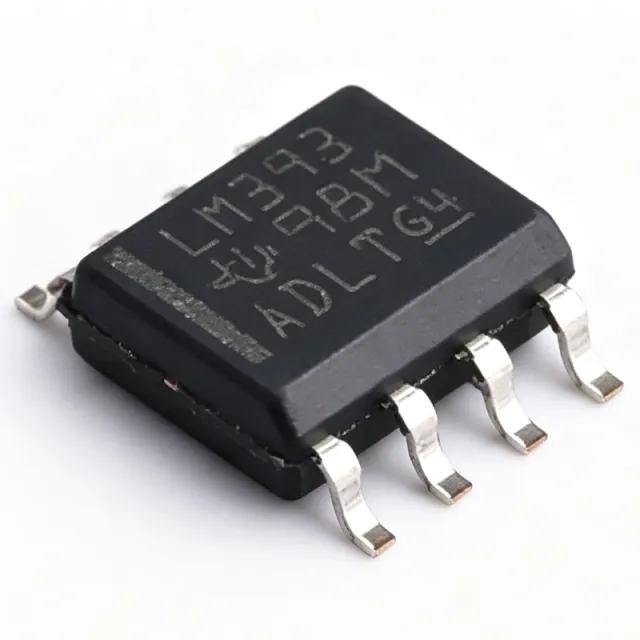
LM393D - Dual Differential Comparator, 36V, Open-Collector SOIC-8 | Texas Instruments (Tape & Reel)
The Texas Instruments LM393D is a dual differential comparator integrating two independent precision comparators on a single monolithic die, housed in an 8-pin SOIC surface-mount package with the industry-standard LM393 pinout. The device operates from a single supply of 2V to 36V or from split dual supplies of plus/minus 1V to plus/minus 18V, and features an open-collector output stage that supports rail-to-rail output swing through an external pull-up resistor. A comparator is an analog building block that compares two input voltages and drives its output to indicate which is greater. Within the component taxonomy, the LM393 belongs to the general-purpose voltage comparator family, sitting as a faster-switching cousin of the operational amplifier optimized for saturated logic-level output rather than linear amplification. It belongs to the signal-conditioning and power-management hierarchy, alongside op-amps, voltage references, and supervisors. Key features include a quiescent supply current of approximately 0.4 mA per comparator that is largely independent of supply voltage, a typical input offset voltage of 1 mV (improved to 0.37 mV on the LM393B revision), and a wide common-mode input range that includes ground (V-), enabling true single-supply ground-sensing. The open-collector output structure allows wired-OR logic and direct interfacing to TTL, CMOS, or any logic family by tying the pull-up to that family's supply rail up to 36V, independent of the comparator's own VCC. The LM393D is built on TI's mature junction-isolated bipolar process with a PNP input stage that gives it the low-input-bias-current robustness expected of a decades-old industry workhorse. Multiple second-source manufacturers including ROHM Semiconductor, STMicroelectronics, ON Semiconductor, and Diodes Incorporated produce pin-compatible LM393D variants, providing true multi-source resilience. The improved LM393B/2903B silicon offers drop-in compatibility with better DC precision and 1 microsecond response time. Typical applications include voltage-level detection, zero-crossing detectors, relaxation oscillators, window comparators, battery undervoltage/overvoltage monitors, and limit comparators in industrial, automotive, and consumer systems. It is also a staple in switched-mode power supply feedback, sensor threshold detection, and as a building block in PWM and 555-style timer circuits. Design consideration: every open-collector output requires a pull-up resistor (typically 1 kOhm to 100 kOhm). Add a few millivolts of positive-feedback hysteresis to prevent output chattering when the input signal transitions slowly through the threshold.
LM393DR - Dual Differential Comparator, 36V, Open-Collector SOIC-8 | Texas Instruments
The Texas Instruments LM393DR is a dual differential comparator integrating two independent precision comparators on a single monolithic die, housed in an 8-pin SOIC surface-mount package with the industry-standard LM393 pinout. The device operates from a single supply of 2V to 36V or from split dual supplies of plus/minus 1V to plus/minus 18V, and features an open-collector output stage that supports rail-to-rail output swing through an external pull-up resistor. A comparator is an analog building block that compares two input voltages and drives its output to indicate which is greater. Within the component taxonomy, the LM393 belongs to the general-purpose voltage comparator family, sitting as a faster-switching cousin of the operational amplifier optimized for saturated logic-level output rather than linear amplification. It belongs to the signal-conditioning and power-management hierarchy, alongside op-amps, voltage references, and supervisors. Key features include a quiescent supply current of approximately 0.4 mA per comparator that is largely independent of supply voltage, a typical input offset voltage of 1 mV (improved to 0.37 mV on the LM393B revision), and a wide common-mode input range that includes ground (V-), enabling true single-supply ground-sensing. The open-collector output structure allows wired-OR logic and direct interfacing to TTL, CMOS, or any logic family by tying the pull-up to that family's supply rail up to 36V, independent of the comparator's own VCC. The LM393DR is built on TI's mature junction-isolated bipolar process with a PNP input stage that gives it the low-input-bias-current robustness expected of a decades-old industry workhorse. Multiple second-source manufacturers including ROHM Semiconductor, STMicroelectronics, ON Semiconductor, and Diodes Incorporated produce pin-compatible LM393DR variants, providing true multi-source resilience. The improved LM393B/2903B silicon offers drop-in compatibility with better DC precision and 1 microsecond response time. Typical applications include voltage-level detection, zero-crossing detectors, relaxation oscillators, window comparators, battery undervoltage/overvoltage monitors, and limit comparators in industrial, automotive, and consumer systems. It is also a staple in switched-mode power supply feedback, sensor threshold detection, and as a building block in PWM and 555-style timer circuits. Design consideration: every open-collector output requires a pull-up resistor (typically 1 kOhm to 100 kOhm). Add a few millivolts of positive-feedback hysteresis to prevent output chattering when the input signal transitions slowly through the threshold.
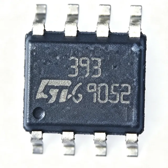
LM393DT - Dual Low-Power Voltage Comparator | STMicroelectronics
The LM393DT is a dual low-power voltage comparator from STMicroelectronics, designed for general-purpose applications requiring precise voltage comparison with minimal power consumption. It operates from a single supply voltage ranging from 2V to 36V or dual supplies from ±1V to ±18V, with a typical supply current of only 0.4 mA per comparator. The device features an open-collector output stage that can sink up to 16 mA, allowing direct interface with TTL, CMOS, and other logic families. The LM393DT is available in the SOIC-8 package, making it suitable for space-constrained PCB designs. Data verified as of 2026-08-05. A voltage comparator is an electronic circuit that compares two input voltages and outputs a digital signal indicating which is higher. The LM393DT is a dual comparator, meaning it contains two independent comparators in a single package. Comparators are fundamental building blocks in analog and mixed-signal systems, used in applications such as threshold detection, zero-crossing detection, and waveform shaping. They are part of the broader category of linear ICs, which also includes operational amplifiers and voltage regulators. The LM393DT's low power consumption and wide supply range make it a versatile choice for battery-powered and industrial applications. Key features of the LM393DT include a low input offset voltage of 2 mV (typical), a low input bias current of 25 nA (typical), and a response time of 1.3 µs (typical) for a 5V overdrive. The open-collector output allows wired-OR connections and level shifting, and the device can operate from a single supply as low as 2V, making it suitable for low-voltage systems. The SOIC-8 package provides a compact footprint with a thermal resistance of 150 °C/W, enabling reliable operation in moderate temperature environments. The LM393DT uses a bipolar transistor architecture with a differential input stage and an open-collector output. This design provides high input impedance and stable operation over a wide temperature range (-40°C to +105°C). The device includes internal ESD protection and is designed to meet JEDEC standards for reliability. The open-collector output requires an external pull-up resistor, which allows the output voltage to be set to any level up to the maximum supply voltage, providing flexibility in interfacing with different logic families. Typical applications for the LM393DT include window comparators, level shifters, oscillator circuits, and analog-to-digital converters. In a window comparator, the dual comparators are used to detect whether an input signal is within a specified voltage range, which is useful in battery monitoring and overvoltage protection. The low power consumption makes it ideal for portable devices, while the wide supply range supports industrial control systems operating from 24V rails. When designing with the LM393DT, ensure that the pull-up resistor is selected to limit the output sink current to within the 16 mA maximum rating. For high-speed applications, minimize parasitic capacitance on the output node to achieve the specified response time. The input common-mode range extends from ground to VCC-1.5V, so ensure that input signals remain within this range for proper operation. This page synthesizes distributor pricing, drop-in alternatives, and practical design notes not found in the STMicroelectronics datasheet, providing a comprehensive resource for engineers selecting and using the LM393DT.
LM393M - Dual Open-Collector Comparator | Texas Instruments
The Texas Instruments LM393M is a dual differential comparator in an 8-pin SOIC package, with two independent comparator channels and open-collector outputs. The verified distributor listing identifies it as a standard general-purpose comparator supporting single-supply or dual-supply operation, with a 2 V to 36 V total supply range and comparator response time listed as 1.4 microseconds. Its open-collector outputs require an external pull-up resistor, allowing the output stage to be wired for wired-AND behavior, level translation, or interface to a higher-voltage logic system. What is a dual differential comparator? A comparator is an analog integrated circuit that compares two input voltages and produces a binary high-or-low result according to their relationship. A differential comparator includes both a non-inverting and an inverting input. The LM393M contains two such channels, making it useful for independent threshold decisions in one package. It belongs to the comparator, analog IC, and semiconductor hierarchy rather than being an amplifier; the output intentionally indicates which input is higher instead of reproducing an analog signal. The key verified feature set includes two differential comparators, an 8-SOIC surface-mount package, open-collector outputs, a 1.4 microsecond response time, and a 2 V to 36 V comparator supply specification. The distributor comparison material also lists differential input and output-current information, while the supplied search results identify the device as suitable for general-purpose comparison. Because the output transistor is open collector, output high level depends on the pull-up resistor and supply rail, not on a push-pull output driver. The two channels are independent, allowing the device to compare two separate sensor or control signals. The common open-collector output architecture can be useful in power-monitoring circuits where several comparator outputs must combine logically, provided the system uses suitable pull-up resistors and does not exceed the device's electrical limits. The SOIC-8 package supports conventional surface-mount assembly, while the dual channel count can reduce board area compared with two single comparators. Typical applications include battery and power-supply monitoring, overvoltage and undervoltage protection, sensor threshold detection, industrial control logic, window or level monitoring, and general digital control systems. The 2 V to 36 V comparator supply range provides useful flexibility for industrial and embedded systems, although the complete operating conditions must be checked against the manufacturer datasheet. A key design consideration is the open-collector output. Add a pull-up resistor to each output, choose its value with the required sink-current and rise-time limits in mind, and ensure that the downstream device accepts the resulting logic level. Do not assume that the output can source current independently. The input common-mode range, output saturation levels, supply current, and absolute maximum ratings are not fully specified in the supplied verified data and must be confirmed before design release. This page combines the verified distributor identity, package information, comparator function, search-result specifications, available cross-reference sources, and practical design guidance. It does not invent unprovided offset, temperature, response-current, or compliance details; unavailable parameters are identified for engineering follow-up.
LM393MX - Dual Open-Collector Comparator, 2-36V | Texas Instruments
Texas Instruments LM393MX is a dual general-purpose differential comparator with open-collector outputs, a 2 V to 36 V supply-voltage range, and an 8-pin SOIC package. The two comparators can operate independently, making the device suitable for voltage-level detection, threshold comparison, window monitoring, and interface conditioning. Verified distributor information identifies the LM393MX as a standard rail-to-rail comparator with a typical response time of 1.3 µs. A comparator is an analog integrated circuit that compares an input voltage with a reference voltage and changes its output state when the relationship between those voltages reverses. The LM393 belongs to the comparator hierarchy within analog and power-management semiconductors. Its open-collector output architecture differs from push-pull or CMOS outputs because the output transistor requires an external pull-up resistor to establish a high voltage. The principal benefits of the LM393MX are its wide 2 V to 36 V operating range, low 1 mA supply current, two independent comparison channels, and open-collector outputs that can support wired logic or interface signaling. The verified data identifies the package as 8-SOIC, making it practical for conventional surface-mount PCB assembly. Its commercial operating-temperature range is listed as 0°C to +70°C. Each channel compares a non-inverting input with an inverting input. When the non-inverting input is higher, the associated open-collector output transistor turns on and pulls the output toward ground. When the non-inverting input is lower, the transistor turns off and the external pull-up resistor raises the output. This behavior allows the output voltage to be established by the system supply and interface rather than by the comparator alone. Typical uses include battery-voltage supervision, industrial sensor thresholds, overvoltage and undervoltage detection, signal conditioning, and control-system interlocks. Its two channels can implement two independent decisions, such as monitoring two regulated rails in one controller. Because the output is open collector, applications must include a suitable pull-up resistor and must account for the sink-current capability of the output transistor. A primary design consideration is that an open-collector output cannot operate as a push-pull logic output without external circuitry. The pull-up resistor determines the rise time, available current, and power loss, while the output node should remain within the voltage limits of the connected logic family. Input common-mode range, output sink current, response time, and offset-voltage limits should be verified in the manufacturer datasheet before using the device outside the verified operating conditions. This page combines the verified manufacturer and distributor specifications, same-package drop-in alternatives, practical comparator design guidance, and application-focused selection information. It also distinguishes verified values from parameters that still require confirmation from the complete LM393 datasheet or a specific alternative manufacturer's documentation.
LM393N - Dual Comparator 2-36V Open-Collector | 8-PDIP
The LM393N is a classic dual low-power low-offset-voltage comparator from the LM193/LM393/LM2903 family originally introduced by National Semiconductor and now multi-sourced by Texas Instruments, Fairchild (onsemi), Motorola, NXP, and others. It integrates two independent precision voltage comparators in an 8-pin PDIP (through-hole, DIP-8) package, designed to operate from a single supply rail of 2 V to 36 V or from split supplies of ±1 V to ±18 V. Each comparator features an open-collector output that can sink up to 16 mA and drives loads referenced to ground or any positive rail up to 36 V, making it ideal for level translation between incompatible logic domains. A comparator is an analog decision element that compares two input voltages and produces a logic-level output indicating which input is larger. The LM393N fits within a hierarchy of: comparator -> analog comparator -> signal-conditioning IC -> semiconductor. Within the broad comparator category, the LM393N belongs to the low-power, low-offset, open-collector-output class (synonym: voltage comparator), distinct from the LM339 quad family and the more modern CMOS comparators such as the LMV393 and LM393LV. Key specifications of the LM393N include: input offset voltage as low as 2 mV maximum (LM193/LM193A series; typical LM393 spec is ±5 mV), input bias current of 25 nA typical, common-mode input range that includes ground, and a propagation delay of approximately 1.3-1.5 microseconds. The open-collector output stage requires a pull-up resistor (typically 2-10 kohm from output to the positive logic rail). The device operates across a -40 C to +85 C ambient temperature range and is widely used in battery-powered systems thanks to its low quiescent current draw (typically 0.4 mA per comparator). Typical applications of the LM393N include zero-crossing detectors for AC line signals, battery voltage monitors and low-battery cutoff circuits, window comparators, over-voltage and over-current protection circuits, square-wave/relaxation oscillators, voltage level shifters (e.g., 5 V CMOS to 12 V relay logic), and analog sensor threshold detectors for photodiodes, thermistors, and Hall-effect sensors. The wide supply range and ground-sensing input make it especially useful in single-rail automotive and industrial 12 V/24 V systems. When designing with this device, remember that the open-collector output cannot actively source current - you must provide a pull-up resistor on each output. Also, the input common-mode range is limited to 0 V to VCC-1.5 V; inputs that approach the upper rail may saturate the input stage. For low-voltage (<5 V) battery applications where lower quiescent current is critical, consider the LMV393 (CMOS) or LM393LV as direct upgrades.
LM393NG - Dual Open-Collector Comparator, 36 V | onsemi
onsemi LM393NG is a dual independent precision voltage comparator with an operating supply range of 2 V to 36 V, housed in an 8-pin PDIP package. The device provides two separate comparator channels, supports single or split supply operation, and uses open-collector outputs. Its input offset voltage is specified as low as 2.0 mV, while the differential input voltage range can extend to ±38 V. The LM393NG is intended for general-purpose industrial, automotive, consumer, and educational designs where two independent threshold or sensing functions are required. A voltage comparator is an analog integrated circuit that compares two input voltages and produces a logic-level indication of their relationship. In the hierarchy of electronic components, the LM393NG is a dual comparator, part of the comparator and analog signal-conditioning family used between sensors, switching circuits, and digital logic. Because its open-collector outputs require an external pull-up resistor, the device can directly interface with TTL, CMOS, and MOS logic while remaining flexible in voltage and polarity. The LM393NG's principal advantages are its two independent channels, low offset voltage of 2.0 mV, 250 nA input current specification, and ability to operate from a single supply or with split supplies. Its common-mode input range includes ground during single-supply operation, making it practical for battery-powered and low-side sensing systems. The open-collector architecture also permits the output transistor to remain off when the device is unpowered, subject to the detailed limits stated by the manufacturer. Technically, the LM393NG combines independent comparator channels with output stages designed for wired-open-collector use. A pull-up resistor sets the output high state, while the comparator pulls the output low when its condition is met. Because the output is not actively driven high, output rise time depends on the pull-up resistance and the capacitance connected to the output node. Designers should therefore avoid excessive pull-up resistance when fast transitions or low propagation delay are important. Typical uses include window monitoring for power rails, sensing battery voltage, comparing a sensor against a reference, detecting overtemperature, building simple oscillator and relay-drive circuits, and generating control signals for industrial or automotive equipment. Split-supply operation is useful where signals may be centered around ground, while single-supply operation supports systems whose available inputs remain between ground and the positive supply. The main PCB considerations are correct orientation, adequate bypassing near the supply pins, and unobstructed pull-up access at each open-collector output. Confirm input common-mode limits, output-current capability, and absolute maximum ratings against the manufacturer datasheet before applying the comparator outside nominal supply conditions. Keep sensitive feedback networks away from switching-node and high-current return paths to avoid offset errors and unstable switching behavior. This page combines the verified onsemi, DigiKey, and Mouser product information with practical comparator-selection guidance, same-package alternatives, and design notes intended to make LM393NG sourcing and implementation decisions more efficient than a basic distributor listing alone.
LM393P - Dual Comparator, 2V-36V, Open-Collector, 8-PDIP | Texas Instruments
The Texas Instruments LM393P is a dual-channel differential comparator with open-collector outputs, housed in an 8-pin PDIP (P) through-hole package. The device contains two independent precision voltage comparators designed to operate from a single supply over a 2V to 36V range, or from dual supplies of ±1V to ±18V, with a typical response time of approximately 1.3 us and a propagation delay of 300 ns. A voltage comparator is a fundamental analog building block that compares two input voltages and produces a digital logic-level output indicating which input is larger. Comparators belong to the broader category of analog comparators -> signal conditioning ICs -> amplifiers and comparators -> analog ICs -> semiconductors. The LM393 family is one of the industry's longest-standing and most widely second-sourced comparator designs, making the LM393P a staple in through-hole commercial, industrial, and educational designs. Open-collector outputs allow the user to define the output high level via an external pull-up resistor to any reference voltage, including a logic level different from VCC, enabling level shifting and OR-wired multi-comparator topologies. Key features include a maximum input offset voltage of ±5 mV, an input bias current of 25 nA typical, a quiescent supply current of 0.4 mA typical (independent of supply voltage), and an open-collector output capable of sinking up to 16 mA. The wide supply range (2V to 36V single supply) and low input bias current make the LM393P well suited to direct interfacing with sensors, op-amp outputs, and TTL/CMOS logic families without additional level translation. Each comparator channel consists of a low-offset differential input stage followed by an open-collector NPN output transistor. The output transistor is OFF when the non-inverting (+) input is at lower potential than the inverting (-) input, and saturates to pull the output LOW when + exceeds -. Designers commonly add an external pull-up resistor (typically 10 kohm to VCC) to establish the HIGH level, which is critical because an open-collector output cannot actively drive HIGH. Typical applications include zero-crossing detectors, over/under-voltage monitors, battery low-detection circuits, window comparators, oscillators, Schmitt triggers, and sensor signal conditioning for industrial, automotive, and consumer designs. The LM393P's through-hole PDIP package supports breadboard prototyping, educational labs, and legacy through-hole PCB designs where surface-mount variants (LM393D, LM393DR) are unsuitable. When designing with the LM393P, place a 0.1 uF bypass capacitor as close as possible to the VCC pin and ensure the pull-up resistor value is sized against the desired output rise time and load capacitance. Avoid driving the output above the maximum collector-emitter voltage of 36V and respect the absolute maximum input common-mode range of -0.3V to VCC to prevent input stage damage. This page synthesizes distributor pricing, drop-in alternatives, and practical design notes not found in the manufacturer datasheet, with verified values drawn from TI product page, DigiKey catalog, and the LM393B/LM2903B datasheet family specification table.
LM393P3 - Dual Open-Collector Comparator | Texas Instruments
Texas Instruments LM393P3 is a dual differential voltage comparator in an 8-pin plastic dual in-line package (8-PDIP). The device provides two independent comparison channels with open-collector outputs, allowing each output to be pulled up to a compatible logic supply and to drive multiple wired-open-collector loads. According to the supplied manufacturer and distributor records, the LM393 family is intended for commercial-grade applications and operates from a 2 V to 30 V supply range, with a 0 °C to 70 °C operating-temperature classification. A comparator is a linear integrated circuit that evaluates two input voltages and produces a logic-level result indicating which input is higher. In the LM393, two comparators share a common supply and ground while retaining separate non-inverting, inverting, and output connections. This dual-channel architecture belongs to the comparator IC hierarchy, where the LM393 occupies the general-purpose, low-power, open-collector segment of the broader analog and power-management semiconductor category. The principal engineering benefit is the open-collector output architecture. Unlike a totem-pole output, an open collector does not actively drive the output high, allowing a pull-up resistor to establish the high logic level. This supports wired-open-collector or wired-AND behavior, permits different supply domains for the pull-up rail, and requires an external pull-up on every output used in a design. The two channels can therefore implement independent threshold decisions, window detection, or complementary comparisons. The LM393P3 uses the standard LM393 differential-comparator architecture rather than rail-to-rail input stages. Input behavior must therefore be evaluated against the device's common-mode and differential input limits in the manufacturer datasheet, especially when comparing signals near either supply rail. Because the verified records do not provide numerical input-offset, response-time, input-bias-current, output-sink-current, or channel-separation figures, those values require confirmation in the official LM393 datasheet before precision timing or sensing decisions are finalized. Typical uses include industrial sensor thresholding, overvoltage and undervoltage detection, battery monitoring, control-loop signal comparison, and digital-interface adaptation. A practical application places the signal under test on one input and a reference voltage from a divider on the other; the open-collector output then changes state when the relation between the two voltages changes. A pull-up resistor converts the output state to a valid logic voltage, while hysteresis can reduce repeated switching when a slowly changing input crosses the reference. For a new design, verify the required output current, input range, temperature grade, and logic compatibility against the datasheet before releasing the schematic. Do not omit the output pull-up resistors, and do not assume that the open collector can source current. Check whether a logic-family or application-specific comparator offers lower offset, faster response, rail-to-rail input operation, push-pull outputs, or automotive qualification. This page combines the verified product records with package, sourcing, comparison, and design guidance focused on drop-in replacement decisions.

LM393PT - Dual Open-Collector Comparator | STMicroelectronics
STMicroelectronics LM393PT is a low-power dual general-purpose voltage comparator with two open-collector outputs, supplied in an 8-pin TSSOP package. The device compares two input voltages and provides a digital, open-drain indication of their relationship, making it suitable for threshold detection, level translation, window monitoring, and simple control systems. Its single-supply architecture supports the positive-voltage signal ranges commonly encountered in industrial and consumer electronics. A voltage comparator is an analog integrated circuit that evaluates one voltage relative to another and changes its output state when the relationship crosses a defined threshold. The LM393 belongs to the comparator IC hierarchy, which sits within interface and signal-conditioning semiconductors. Unlike an operational amplifier configured as a comparator, the LM393 integrates an open-collector output stage intended for wired logic, relay drivers, and systems that need pull-up resistors. The principal feature of the LM393PT is its dual-channel architecture, allowing two independent comparisons in one package. Both channels use open-collector outputs, so each output can pull a logic rail low while presenting a high-impedance state when inactive. The verified distributor description identifies the device as a standard general-purpose, rail-to-rail comparator, although detailed input common-mode, output-current, timing, and supply-current limits require confirmation from the manufacturer datasheet. The 8-pin TSSOP package supports compact PCB layouts while exposing both comparator channels, their input pins, the common supply connection, and both output pins. Because the outputs are open collector, an external pull-up resistor is normally required on each output. That arrangement supports wired-AND behavior at the logic interface and permits the output node to be pulled toward a voltage selected by the application rather than being forced to the comparator supply voltage. Typical uses include battery-threshold detection, industrial control-interface qualification, sensor-limit switching, overvoltage and undervoltage monitoring, and general digital threshold generation. The dual-channel configuration can implement two independent alarms or form the two comparisons required by a window comparator when suitable threshold references and output logic are added. A critical implementation consideration is the required output pull-up: omitting it leaves the open-collector output floating. Designers should also verify input voltage limits, output sink-current capability, propagation delay, input-offset behavior, and supply operating range against the STMicroelectronics datasheet before applying the comparator outside its published conditions. This page combines verified distributor specifications and sourcing information with a package-specific pinout, drop-in replacement analysis, comparison data, and practical design guidance. It is intended to support faster component selection while clearly separating confirmed LM393PT attributes from electrical parameters that still require datasheet verification.

LM393TL - Dual Open-Collector Comparator, 2-36V | Texas Instruments
The Texas Instruments LM393TL is a dual differential voltage comparator with open-collector outputs, supplied from 2 V to 36 V (±1 V to ±18 V) and packaged in an 8-WFBGA (8-DSBGA) surface-mount package supplied in tape-and-reel. Each of the two independent comparator channels offers an input offset voltage of up to 9 mV (9000 uV) and a response time of 1300 ns. A comparator is a differential amplifier that converts the voltage difference between two inputs into a logic-level output. As part of the wider signal-conditioning chain, a comparator sits between sensor front-ends and digital logic, in the hierarchy analog IC -> comparator -> differential input stage -> signal conditioning. The LM393 family is the classic open-collector (open-drain) dual comparator used for threshold detection, zero-crossing sensing and open-drain bus interfacing. Key features of the LM393TL include a very wide 2 V to 36 V single supply range (or ±1 V to ±18 V split supply), an input common-mode range that includes ground, a differential input voltage range of ±38 V, and outputs compatible with TTL, CMOS and MOS logic families. Because the outputs are open collector, a single external pull-up resistor per channel is required to establish a logic high, which also allows wired-AND busing and level shifting. Internally the LM393 is built around a classic bipolar differential input stage driving a large-area open-collector output transistor. The wide input common-mode range and low supply current make the part suitable for slow, cost-sensitive sensing rather than high-speed signal conditioning; the 1300 ns response time reflects the open-collector architecture rather than any limitation of the input stage. Typical applications include battery-powered threshold detection, over/under-voltage and temperature monitoring in industrial and consumer equipment, zero-cross detection in AC mains and motor control, and open-drain level shifting between 5 V TTL systems and 3.3 V CMOS logic. Design consideration: because the LM393TL output is open collector, always fit a pull-up resistor (typically 2 kΩ to 10 kΩ) close to the device, and check that the pull-up rail voltage does not exceed the absolute maximum ratings of the output transistor. Note also that the commercial-grade LM393 is rated 0 °C to 70 °C; use LM2903 for industrial temperature ranges. This page combines verified distributor and manufacturer data with package-specific alternatives, a parameter comparison table, and practical layout notes that are not found in the original manufacturer datasheet, giving engineers a faster path from part selection to a working PCB.

LM4871MX/NOPB - 3W Mono Class-AB Audio Amp | Texas Instruments
The LM4871MX/NOPB is a mono bridged audio power amplifier from Texas Instruments, part of the Boomer series, capable of delivering 3W of continuous average power into a 3Ω load with less than 10% THD when powered by a 5V supply. It operates from a 2V to 5.5V supply, making it ideal for battery-powered portable devices. The device features a shutdown mode that reduces quiescent current to minimize power consumption when not in use. Housed in an 8-pin SOIC (D) package, it is designed for surface-mount assembly and operates over a temperature range of -40°C to 85°C. An audio power amplifier is an electronic amplifier that amplifies low-power audio signals to a level suitable for driving loudspeakers. The LM4871 is a Class-AB amplifier, which offers a good compromise between efficiency and linearity, providing low distortion while consuming moderate power. In the hierarchy of audio electronics, it falls under audio amplifiers, which are a subset of analog ICs used in consumer electronics, portable devices, and multimedia systems. Key features include a shutdown mode with low quiescent current (6.5mA typical), a wide supply voltage range of 2V to 5.5V, and a maximum output power of 3W into 3Ω. The device also offers thermal shutdown protection and is available in a lead-free (NOPB) version, compliant with RoHS. Its differential output architecture eliminates the need for output coupling capacitors, reducing external component count and board space. The LM4871 uses a bridged-tied load (BTL) configuration, which effectively doubles the voltage swing across the load compared to a single-ended amplifier, maximizing output power without increasing supply voltage. This architecture, combined with a low-noise design, ensures clean audio reproduction. The device is designed for simplicity, requiring only a few external components, making it easy to integrate into compact designs. Typical applications include portable speakers, mobile phones, MP3 players, and other battery-powered audio devices where high efficiency and low power consumption are critical. Its small SOIC package and minimal external component requirement make it suitable for space-constrained designs. When designing with the LM4871, ensure proper PCB layout with adequate ground plane and decoupling capacitors close to the supply pins to minimize noise and improve thermal performance. The shutdown pin can be used for power management to extend battery life.
LM4875M/NOPB - 750mW Mono Audio Amplifier w/ DC Volume | TI
The Texas Instruments LM4875M/NOPB is a 750 mW mono bridged audio power amplifier with DC voltage volume control and headphone switch, housed in an 8-pin SOIC package. It operates from a 2.7 V to 5.5 V supply, delivers 750 mW continuous average power into an 8 ohm load at less than 1% THD+N when powered from 5 V, and integrates a mono Class-AB output stage with a dedicated single-ended headphone channel. The die combines the speaker amplifier, headphone amplifier, depop circuitry, and a digitally-controlled analog volume interface in a single 8-pin SOIC footprint. An audio power amplifier IC is an integrated circuit that delivers sufficient low-distortion current to drive a loudspeaker or headphone transducer from a low-voltage analog source. Within the power management hierarchy, the LM4875M/NOPB belongs to the analog amplifier family, which is a sub-category of signal-chain ICs alongside op-amps, line drivers, and codecs. Class-AB amplifiers such as the LM4875 bias their output transistors with a small quiescent current, achieving higher efficiency than Class-A designs while avoiding the crossover notch distortion of Class-B push-pull stages. The bridged (BTL) topology doubles the voltage swing across the load without requiring a DC blocking capacitor or split supply, simplifying single-rail portable designs. Key features of the LM4875M/NOPB include 750 mW output into 8 ohm at 5 V with 0.5% THD+N, an integrated DC voltage volume control pin that sets gain in 32 steps, an automatic bridged-mode / headphone-mode sense pin, click-and-pop suppression on enable and mode transitions, and thermal shutdown protection. The supply range of 2.7 V to 5.5 V supports both single-cell Li-ion (3.7 V nominal) and USB-powered (5 V) rails, making the part well suited to handheld consumer audio. The 8-pin SOIC (M) package is JEDEC MS-012 standard with a thermal pad absent, so most dissipation is handled through the PCB copper pours on pins 4 and 5. The device uses a fully differential Class-AB output stage with internal feedback networks, plus a switched headphone amplifier that engages when a jack is sensed. Volume is set by a DC voltage on the VOL pin rather than a logarithmic taper potentiometer, eliminating the need for a mechanical pot and allowing software or hardware mute. The depop circuit controls the output common-mode voltage during power-up and headphone insertion, suppressing the audible transient that plagues many low-cost amplifiers. Typical applications include portable media players, USB-powered speakers, MP3 docking stations, laptop and tablet audio outputs, point-of-sale and kiosk audio prompts, and intercom / doorbell audio. The wide 2.7-5.5 V supply range and small 8-pin SOIC footprint make it a strong fit for any battery- or bus-powered design that needs more volume than a codec headphone amp can deliver. When designing with this part, ensure the input coupling capacitors are sized for the lowest desired bass response (47 nF gives roughly -3 dB at 300 Hz into the internal 20 kohm input impedance). Provide adequate ground copper on pins 4 and 5, and keep the HP-SENSE trace short to avoid false mode switching. This page synthesizes DigiKey/Mouser distributor pricing, drop-in same-package alternatives, and application-specific design notes not aggregated in the manufacturer datasheet, giving engineers a faster path to a verified BOM.

LM7321MFX/NOPB - 32V 20MHz RRIO Op Amp SOT-23-5 | TI
The Texas Instruments LM7321MFX/NOPB is a single-channel, rail-to-rail input and output (RRIO) operational amplifier delivering 20-MHz unity-gain bandwidth, 18-V/us slew rate, and up to 65 mA of output current from a compact 5-pin SOT-23 (DBV) package. It operates from supplies of 2.5V to 32V (up to +/-16V dual supply) while drawing only about 1 mA of supply current per amplifier. An operational amplifier (op amp) is a high-gain voltage amplifier used in the analog signal chain hierarchy: amplifier IC -> general-purpose op amp -> precision analog front end. The LM7321 belongs to the rail-to-rail op amp class, whose input and output stages swing to within millivolts of both supply rails, maximizing dynamic range in low-voltage and single-supply systems. Key differentiating features include unlimited capacitive load stability - the output drives large capacitive loads directly without external compensation - plus the high 65-mA output current that allows the device to drive heavy loads such as coaxial cables, ADC inputs, and actuator drivers. The rail-to-rail I/O architecture maintains performance across the full 2.7V, +/-5V, and +/-15V operating points specified by TI, and the wide temperature range of -40C to +125C supports industrial and automotive-adjacent designs. Internally, the LM732xx family uses a complementary input stage that seamless transfers near the rails, preserving bandwidth and phase margin across the common-mode range. The combination of 20-MHz bandwidth with only 1-mA quiescent current yields an excellent bandwidth-to-power figure compared with general-purpose parts such as the LM358. Typical applications include video and coaxial cable drivers, ADC input buffering, active filters, piezo and capacitive load drivers, test-and-measurement signal conditioning, and battery-powered portable instrumentation. The NOPB suffix indicates RoHS-compliant, lead-free terminations. Design tip: while capacitive load stability is essentially unlimited, keep supply decoupling close to the pins (100 nF per rail) and beware of thermal limits when sourcing 65 mA continuously at high output voltage swing.
LM741-MIL - General-Purpose Operational Amplifier | Texas Instruments
The Texas Instruments LM741-MIL is a general-purpose operational amplifier intended for a wide range of analog applications. Its verified product information identifies improved performance over industry standards such as the LM709, while the listed package and detailed electrical values are not supplied in the retrieved web data. The device is associated with the LM741 series, a classic single-amplifier architecture used in integrator, summing-amplifier, and general-feedback circuits. An operational amplifier is an integrated circuit that uses high-gain differential amplification with negative feedback to create predictable closed-loop behavior. The LM741 family belongs to the broader operational-amplifier, analog-amplifier, signal-conditioning, and semiconductor categories. Its general-purpose positioning makes it relevant to educational circuits, laboratory instruments, audio signal paths, analog control systems, filters, amplifiers, and legacy equipment where an established 741-family pinout and application ecosystem may be important. According to the verified Texas Instruments product-page information, the LM741-MIL provides improved performance relative to the LM709 and is a direct plug-in replacement for the 709C, LM201, MC1439, and 748 in most applications. The same source states that its high gain and wide operating-voltage range support integrator, summing-amplifier, and general-feedback applications. Exact supply voltage, input common-mode range, output swing, gain-bandwidth product, slew rate, input bias current, offset voltage, noise, and temperature-range values are not included in the supplied evidence and therefore must be verified from the manufacturer datasheet before design use. The verified Mouser result further describes the LM741-MIL as an operational amplifier for wide-ranging analog applications. The retrieved sources also identify the manufacturer as Texas Instruments and provide links to the product page and datasheet. Because the supplied data does not establish a precise orderable package suffix, pin count, lead-free status, automotive qualification, lifecycle classification, or distributor price, those fields remain data-needed rather than inferred. Typical circuit uses include closed-loop non-inverting and inverting amplifiers, analog summing networks, active filters, integrators, transducers, and general feedback control blocks. Designers should preserve the package and pinout of the installed circuit, confirm the applicable electrical limits, and verify stability, biasing, output swing, and compensation requirements before substituting a modern amplifier. This page summarizes only verified web information and avoids adding undocumented electrical claims. For a new high-precision design, compare the LM741-MIL against modern rail-to-rail input and output amplifiers, because the LM741’s historical architecture is not automatically the best choice for low-voltage or high-speed systems. For an existing legacy board, use the verified direct-plug-in-replacement claim only after checking the exact package and pin arrangement against the current schematic and datasheet.