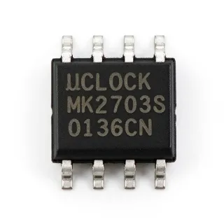
ICS501AMI - 166MHz Clock Generator IC | Renesas | SOIC-8
MPN: ICS501AMI ✓ AktifICS501AMI Genel Bakış
A clock generator is a timing IC that converts or multiplies a lower-frequency reference into a higher-frequency clock for digital logic, processors, communications equipment, and embedded control systems. Within the clock and timing hierarchy, the ICS501AMI belongs to the clock-generator and PLL-clock-multiplier class, combining a frequency reference with a phase-locked loop. It differs from a conventional oscillator because it does not require a complete resonator-and-amplifier arrangement when an external reference is available.
The ICS501A architecture supports generation of a high-quality, high-frequency clock output from a lower-frequency crystal or clock input. Its stated maximum operating frequency is 166MHz, while CMOS-compatible clock signaling integrates with modern digital systems. Operating from a single low-voltage supply keeps the implementation compact, although the exact supply-voltage limits, current consumption, output jitter, lock-range limits, and temperature ratings should be confirmed against the manufacturer datasheet before release to production.
A typical implementation places the low-frequency reference at the timing input, connects the required support components, and routes the multiplied clock to the destination logic. The crystal or reference circuit must satisfy the frequency and load requirements stated in the manufacturer datasheet. PCB layout, grounding, and supply bypassing become increasingly important as the output frequency rises because clock-edge jitter and power-supply noise can reduce system timing margin even when the nominal output frequency is correct.
ICS501AMI is appropriate for digital control systems, embedded processing, industrial electronics, communications equipment, and retrofit designs that use the established ICS501 footprint. It can also serve clock-tree distribution when an existing reference signal should be reused. For battery-powered equipment, compare the device's operating current and idle behavior against system power budgets. In systems requiring precise synchronization among multiple domains, first confirm the device's PLL lock behavior and output stability under the intended reference conditions.
Use the manufacturer's pin-description table when assigning PCB tracks, and preserve the documented bypass-capacitor layout to minimize supply noise at the clock pins. Verify startup, reference stability, output waveform, and maximum operating frequency across the full intended temperature range. This page combines the available manufacturer and distributor information with practical implementation guidance, sourcing questions, and clearly qualified same-package alternatives for design review.
Drop-in alternatifler için ICS501AMI — aynı paket, pin-başına uyumlu. PCB yeniden montajı gerektiren farklı paket bileşenleri dışlanmıştır.
501AMILF
✅ Yerleştirme📋 Katalogda Olmayan Referans Alternatifi
ICS501AMILFT
✅ Yerleştirme📋 Katalogda Olmayan Referans Alternatifi
ICS501AMI Özellikler
| Device Type | Clock Generator IC |
| Product Family | ICS501A LOCO |
| Azami Saat Hızı | 166 MHz |
| Clock Logic | CMOS |
| Package Type | 8-SOIC |
| Package Width | 0.154 inch (3.90 mm) |
| Montaj Türü | Surface Mount |
| RoHS Durumu | unknown |
| REACH Status | unknown |
| AEC-Q100 Qualification | not_applicable |
ICS501AMI 0.154 inch (3.90 mm) Pin Yapısı Kılavuzu
ICS501AMI (0.154 inch (3.90 mm) paket) için pin yapısı. Pin numaralandırma, işlevleri ve bağlantı şemaları üretici veri kitapçığında tanımlanmıştır. Doğru ayak ve soldurma kılavuzları için onu referans alın.

Ayrıntılı pin çıkış verisi mevcut değil: ICS501AMI.
Aşağıdaki veri sayfası tam pin konfigürasyonu için.
Tipik Uygulamalar
ICS501AMI için uygundur 6 uygulamas: Embedded Processor Clocking, Industrial Control Clock Tree, Communications Module Timing, Data Converter and Interface Timing, Test and Measurement Front Ends, Legacy Equipment Repair.
Embedded Processor Clocking
ICS501AMI fits embedded processor designs that already include a low-frequency crystal or clock source but need a higher-frequency operating clock. The ICS501A LOCO architecture uses a PLL clock multiplier to derive up to 166MHz, reducing the need for a separate high-frequency crystal-oscillator assembly. Place the device close to the reference source, use the recommended bypass components, and validate startup and lock behavior with the actual reference frequency. The main engineering consideration is timing margin: the processor clock must meet its frequency, jitter, and duty-cycle requirements rather than merely matching the nominal output value.
Önerilen
Industrial Control Clock Tree
ICS501AMI is applicable to industrial control equipment where a stable system reference can be reused for processor, logic, and communications timing. Its 166MHz maximum output rating and CMOS clock interface support high-rate digital sections, while the 8-SOIC package allows conventional surface-mount assembly. A robust design should isolate the reference and clock traces from switching power stages and motors, provide local supply bypassing, and test PLL acquisition after power-up. Confirm the exact operating limits and lifecycle plan with the Renesas Electronics manufacturer datasheet before using the part in new industrial production equipment.
Önerilen
Communications Module Timing
ICS501AMI can provide a multiplied clock in communications modules when a lower-frequency reference is available from another system block. A clock output of up to 166MHz can support digital processing and interface circuitry, provided the selected PLL configuration covers the required output and the source remains stable under changing operating conditions. Keep the clock path short, maintain a continuous ground reference, and avoid routing it beside high-energy RF or switching-supply traces. Review output jitter, duty-cycle distortion, load capacitance, and maximum frequency in the manufacturer datasheet before sign-off because nominal frequency alone does not establish interface timing margin.
Önerilen
Data Converter and Interface Timing
ICS501AMI is suitable for generating the interface clock used by data converters, digital logic, or interface controllers when the board contains a suitable reference source. Its CMOS output and maximum rated frequency make it a candidate for mid-speed digital trees, but the receiving device's setup and hold requirements remain decisive. Engineers should compare jitter and skew against the complete clock and data budget rather than relying on frequency alone. Use short traces, matched reference grounding, and manufacturer-recommended decoupling, and verify that the output load remains within the device's specified drive capability.
Önerilen
Test and Measurement Front Ends
ICS501AMI can serve as a local clock multiplier in test and measurement front ends that require a higher-rate digital clock derived from a stable laboratory reference. The 166MHz capability is useful for sampling control, digital signal processing, or interface timing, provided the source frequency is within the PLL operating range. Keep the oscillator and clock generator on a quiet analog or mixed-signal section, provide local decoupling, and account for the reference's phase noise and amplitude tolerance. The design should also include startup and lock checks, especially in remote or automated test systems where a failed clock can invalidate measurements.
Önerilen
Legacy Equipment Repair
ICS501AMI is particularly useful for maintaining established equipment that already uses its 8-SOIC footprint and requires the ICS501A clock-multiplier function. The existing PCB can benefit from a direct-form replacement when the reference frequency, supply, pin functions, and multiplier configuration match the original design requirements. Before ordering, compare the candidate's absolute maximum ratings and timing behavior with the installed circuit and verify availability for the intended production horizon. In service applications, preserve the original reference-network and decoupling layout because component substitution cannot compensate for degraded crystals, excessive loading, or poorly controlled supply noise.
Önerilen
Önerilen Ürünler Özeti
Mühendislik referans verileri: ICS501AMI — karşılaştırma, tasarım rehberi ve uyumluluk bilgileri.
Seçim Kılavuzu
Alternatiflerle Karşılaştırma
| Parametre | Bu Ürün | 501AMILF | ICS501AMILFT |
|---|---|---|---|
| Brand | Renesas Electronics | Renesas Electronics | Renesas Electronics |
| Package | 8-SOIC | 8-SOIC | 8-SOIC |
| Device Type | Clock Generator IC | Clock Generator | Clock Generator |
| Function | ICS501A LOCO PLL clock multiplier | Clock generator | ICS501A LOCO clock generator and multiplier |
| Reference Input | Lower-frequency crystal or clock input | Lower-frequency crystal or clock input | Lower-frequency crystal or clock input |
Ana Farklılayıcılar
- Established ICS501A clock-multiplier function (karşılaştırma:501AMILF)
- Same-package continuity for compatible designs (karşılaştırma:ICS501AMILFT)
- Documented lower-frequency reference capability (karşılaştırma:501AMILF)
Tasarım Notları
Place ICS501AMI close to the crystal or external clock source and route the reference path as a short, continuous trace. Keep the clock-output path isolated from switching-regulator nodes, relay drivers, and high-current digital return paths. Use a continuous ground plane and manufacturer-recommended bypass components at the supply pins. The exact crystal-load network and component placement should follow the Renesas Electronics manufacturer datasheet rather than a generic reference-circuit example.
Treat the multiplied clock as a high-speed signal even though its source is a low-frequency reference. Avoid stubs, test-point discontinuities, and unnecessary layer changes, and provide a nearby return path. Verify rise time, duty-cycle distortion, jitter, and load capacitance on the assembled PCB. A nominal 166MHz output does not by itself guarantee adequate timing margin; compare the measured clock against the receiving device's setup, hold, and jitter specifications.
Do not select a replacement from package similarity alone. Confirm pin functions, reference-input range, multiplier ratio, PLL lock behavior, supply limits, output-drive capability, and temperature grade in the manufacturer datasheet. When substituting 501AMILF or ICS501AMILFT for ICS501AMI, validate startup from a cold power cycle and verify that the output remains locked when the reference changes. A working bench sample should not replace application-specific timing and qualification testing.
Uyumluluk Bilgisi
The available product information does not state RoHS, REACH, lead-free, halogen-free, or conflict-minerals status. ICS501AMI is a general-purpose clock and timing IC rather than an automotive-qualified device.