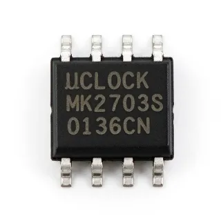
ICS508MT - 250 MHz PECL-to-CMOS Clock Converter | Renesas
MPN: ICS508MT ✓ AktifICS508MT Genel Bakış
A clock converter is an interface IC within the clock and timing hierarchy, where clock-generation and clock-buffer functions support digital logic, communications, and signal-processing systems. PECL, or positive emitter-coupled logic, is a high-speed differential signaling format, while CMOS provides a single-ended output suitable for driving conventional digital circuitry. The ICS508MT bridges these electrical domains without using a PLL.
Key features include a 250 MHz maximum clock frequency, one converter circuit, a 1:1 input-to-output ratio, and separate VDD supplies for voltage translation. Differential clock input supports noise-resistant high-speed transmission, while the CMOS output provides a compatible signal for downstream digital logic. The absence of a PLL also means no multiplication or division function is added by this device.
Technically, the ICS508MT is a clock translator rather than a frequency synthesizer. It preserves the input clock relationship at its output while changing the interface from differential PECL to single-ended CMOS. Separate supply domains allow the input and output circuitry to operate from different supply voltages, which is useful when connecting clock sources and logic devices that use different rail levels. Designers must still provide suitable decoupling and high-speed routing between the source, converter, and receiving logic.
Typical applications include telecommunications and data-communications clock distribution, high-speed digital backplanes, FPGA clock interfaces, network equipment, and test instrumentation. The part is particularly appropriate when a board contains a PECL clock source but the receiving logic requires a CMOS-compatible clock.
When designing around the ICS508MT, prioritize short, controlled impedance traces, solid grounding, and manufacturer-recommended bypass capacitors. Check that the PECL common-mode and termination arrangement matches the clock-source requirements, and verify the output supply and logic thresholds against the downstream device.
This page combines the defining ICS508MT specifications, practical interface guidance, and verified drop-in alternatives. It also distinguishes the device from true clock generators and PLL-based converters so engineers can select it according to interface, frequency, packaging, and supply-domain requirements.
Drop-in alternatifler için ICS508MT — aynı paket, pin-başına uyumlu. PCB yeniden montajı gerektiren farklı paket bileşenleri dışlanmıştır.
ICS508M
✅ YerleştirmeFiyat için iletişime geçin
Veri Şablonunu Görüntüle →ICS508
✅ Yerleştirme📋 Katalogda Olmayan Referans Alternatifi
ICS508MT Özellikler
| Product Type | PECL-to-CMOS clock converter |
| Azami Saat Hızı | 250 MHz |
| Number of Circuits | 1 circuit |
| Input-to-Output Ratio | 1:1 |
| Input Logic | Differential PECL |
| Output Logic | Single-ended CMOS |
| Differential Input | Yes |
| Differential Output | No |
| PLL | No |
| Supply Architecture | Separate VDD supplies for voltage translation |
| Paket | 8-SOIC |
| Package Body Width | 3.90 mm |
| Package Length | 0.154 inch |
| Pin Sayısı | 8 pins |
| Montaj Türü | Surface mount |
| Datasheet Publication Date | 1999-05-22 |
ICS508MT 0.154 inch Pin Yapısı Kılavuzu
ICS508MT (0.154 inch paket) için pin yapısı. Pin numaralandırma, işlevleri ve bağlantı şemaları üretici veri kitapçığında tanımlanmıştır. Doğru ayak ve soldurma kılavuzları için onu referans alın.

Ayrıntılı pin çıkış verisi mevcut değil: ICS508MT.
Aşağıdaki veri sayfası tam pin konfigürasyonu için.
Tipik Uygulamalar
ICS508MT için uygundur 6 uygulamas: Telecommunications Clock Distribution, FPGA Clock Interface, High-Speed Network Equipment, High-Speed Digital Backplane, Test and Measurement Instrumentation, Clock Translation Between Mixed Logic Domains.
Telecommunications Clock Distribution
The ICS508MT fits telecommunications equipment that uses a differential PECL clock source but requires a single-ended CMOS clock at a downstream logic or interface device. Its 250 MHz maximum frequency and 1:1 ratio preserve the source timing while converting the electrical format. Separate VDD supplies allow the PECL-side and CMOS-side voltage domains to be established independently. Place the converter close to the receiving logic, use short return paths, and verify the source common-mode and termination requirements to minimize data-dependent jitter and edge degradation.
FPGA Clock Interface
The ICS508MT is applicable when an FPGA or other digital logic cannot use the available differential PECL clock directly. The device converts the source into a single-ended CMOS clock with a maximum stated frequency of 250 MHz and no frequency multiplication or division. This makes the interface deterministic and suitable for clock transfer between incompatible logic families. Check the FPGA input threshold, maximum operating frequency, supply voltage, and jitter tolerance, and keep the CMOS output route short to minimize added susceptibility to board noise.
High-Speed Network Equipment
Network and data-communications chassis commonly combine high-speed differential clocking with CMOS control logic. ICS508MT provides a compact interface between those domains without introducing a PLL or changing the clock ratio. Its one-channel architecture is appropriate where a single translated clock is needed, and the 8-SOIC package supports conventional surface-mount assembly. The principal design considerations are clean supply decoupling, controlled return-current paths, and compliance with the PECL source's termination and common-mode requirements.
High-Speed Digital Backplane
ICS508MT can be used at a backplane boundary where a PECL-based clock distribution reaches a board containing CMOS logic. The converter preserves the clock through a 1:1 ratio while producing a conventional CMOS output, allowing the clock function to remain distributed across a mixed-interface architecture. Since propagation delay and edge quality affect board-to-board timing, engineers should evaluate the complete clock path and use controlled impedance rather than treating the interface conversion as an isolated component choice.
Test and Measurement Instrumentation
The ICS508MT can bridge a PECL test-clock source into CMOS instrumentation when the instrument uses single-ended clock inputs. The 250 MHz capability supports high-speed laboratory and production-test systems, while the 1:1 ratio keeps the output frequency directly traceable to the source. Use short PCB routing and stable bypass capacitance to preserve edge quality, and confirm that the downstream instrument accepts the resulting CMOS amplitude and timing specification.
Clock Translation Between Mixed Logic Domains
ICS508MT is useful in mixed-signal and mixed-logic systems where a PECL clock must be translated for a CMOS receiver. Separate VDD supplies provide the mechanism for voltage translation, while the single-ended output supports ordinary CMOS clock inputs. The converter does not synthesize a new frequency, so a stable upstream clock and suitable signal integrity remain essential. A practical implementation should include local decoupling, a continuous ground reference, and deliberate routing that minimizes loop area and susceptibility to adjacent switching noise.
Mühendislik referans verileri: ICS508MT — karşılaştırma, tasarım rehberi ve uyumluluk bilgileri.
Seçim Kılavuzu
Alternatiflerle Karşılaştırma
| Parametre | Bu Ürün | ICS508M | ICS508 |
|---|---|---|---|
| Brand | Renesas Electronics | Renesas Electronics | Renesas Electronics |
| Package | 8-SOIC | 8-SOIC | 8-SOIC |
| Maximum Frequency | 250 MHz | 250 MHz | 250 MHz |
| Product Function | PECL-to-CMOS converter | Clock generator interface | PECL-to-CMOS converter |
Ana Farklılayıcılar
- Direct PECL-to-CMOS interface conversion (karşılaştırma:ICS508M)
- No PLL or frequency conversion stage (karşılaştırma:ICS508)
- Separate supply domains for interface translation (karşılaştırma:ICS508M)
- Single-channel implementation in a compact 8-SOIC (karşılaştırma:ICS508)
Tasarım Notları
Treat the PECL input as a controlled high-speed differential connection. Follow the source and manufacturer termination recommendations, maintain a continuous reference plane, and minimize the loop between the clock source, ICS508MT, and the receiver. The 1:1 ratio avoids frequency-changing logic, but edge distortion and jitter introduced by routing can still affect the receiving CMOS device.
Use separate local bypass paths for the input and output VDD domains because the principal function of the ICS508MT is voltage translation. Place the required capacitors close to their associated supply pins and keep return-current paths continuous. Verify both supply voltages against the absolute maximum and recommended operating limits in the manufacturer datasheet before energizing the circuit.
Route the single-ended CMOS output as a short clock trace directly toward the receiving logic, with a continuous ground reference and no unnecessary stubs. Avoid placing the converter near unrelated high-current switching nodes when clock quality is critical. If the receiver is physically distant, use an appropriate clock-buffer or retiming strategy instead of extending a sensitive clock trace across the board.
Do not treat ICS508MT as a frequency synthesizer or jitter cleaner. It has a 1:1 input-to-output ratio and no PLL, so it cannot correct a poor source clock or create a required output frequency. Confirm the source amplitude, common mode, duty cycle, jitter, and maximum frequency, and verify the CMOS output amplitude and timing against the receiving device.
Uyumluluk Bilgisi
The manufacturer datasheet is dated 1999-05-22, but no explicit RoHS, REACH, lead-free, halogen-free, or conflict-minerals declarations were identified.