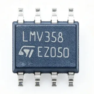
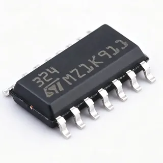
L2726013TR - 28V 1.2MHz Dual Op Amp | STMicroelectronics
MPN: L2726013TR ✗ Son Kullanım ZamanıL2726013TR Genel Bakış
A power operational amplifier is a general-purpose amplifier designed to operate from single or split supplies while providing relatively high output-current capability. It belongs to the operational-amplifier hierarchy, where an operational amplifier functions as a voltage-controlled voltage source with very high open-loop gain, high input impedance, and low output impedance. The L27260 series adds low-dropout operation, broad common-mode and differential-mode input ranges, and output-current capability suited to instrumentation and buffering applications.
The L2726013TR supports single or split supply operation, with a minimum supply magnitude of 2 V. Typical split-supply configurations include ±3 V, ±5 V, ±9 V, and ±12 V, while its 28 V rating supports higher total-voltage applications. Its 1.2 MHz bandwidth supports general-purpose amplification at moderate frequencies. Thermal shutdown and internal clamp diodes provide additional protection against excessive junction temperature and output overdrive conditions.
Two amplifiers in one package make the L2726013TR useful for dual-channel signal paths. A typical instrumentation channel can use one amplifier for input conditioning and the other for active filtering or output buffering. The device can also implement differential-to-single-ended conversion, comparator-style thresholding with appropriate feedback, gain stages, and bridge-sensor excitation interfaces. Ground-compatible inputs allow operation from circuits referenced close to the lower supply rail.
Typical applications include low-frequency instrumentation, audio and communication buffers, power-converter control loops, sensor interfaces, active filters, and industrial measurement systems. The 1 A output-current capability is particularly useful where the source must charge or discharge larger output capacitances, although stability should be verified for capacitive loads. The SO-20 footprint also allows both amplifier circuits to be placed in one compact surface-mount package.
Design attention should focus on supply headroom, output-current limits, thermal dissipation, and feedback-loop stability. Use the manufacturer datasheet's pinout and recommended application circuit when assigning inputs, outputs, supplies, and compensation connections. Avoid driving highly capacitive loads without checking the recommended compensation network, and calculate worst-case dissipation across the full operating temperature range.
This page organizes the L2726013TR's core electrical characteristics, practical application fit, package information, verified source links, and constrained drop-in alternatives. It also highlights where engineers should compare the datasheet limits directly against application requirements before substituting a different amplifier or reusing an existing SO-20 layout.
Drop-in alternatifler için L2726013TR — aynı paket, pin-başına uyumlu. PCB yeniden montajı gerektiren farklı paket bileşenleri dışlanmıştır.
L2726013TR-LF
✅ Yerleştirme📋 Katalogda Olmayan Referans Alternatifi
L2726013
✅ Yerleştirme📋 Katalogda Olmayan Referans Alternatifi
L2726
✅ Yerleştirme📋 Katalogda Olmayan Referans Alternatifi
L2726013TR Maksimum Değerlendirmeler & Elektriksel Özellikler
| Amplifier Type | Dual general-purpose operational amplifier |
| Number of Circuits | 2 circuits |
| Gain-Bandwidth Product | 1.2 MHz |
| Maximum Supply Voltage | 28 V |
| Minimum Supply Voltage | ±2 V split supply |
| Typical Supply Voltages | ±3 V, ±5 V, ±9 V, or ±12 V split supply |
| Maksimum Çıkış Akımı | 1 A per amplifier |
| Maximum Power Dissipation | 1000 mW |
| Supply Configuration | Single or split supply |
| Thermal Protection | Thermal shutdown |
| Output Protection | Internal clamp diode |
| Temperature Grade | Industrial |
| Paket | SO-20, 20 terminals, gull-wing lead form |
| Montaj Türü | Surface mount |
| Number of Terminals | 20 |
L2726013TR so-20, 20 terminals, gull-wing lead form Pin Yapısı Kılavuzu
L2726013TR (so-20, 20 terminals, gull-wing lead form paket) için pin yapısı. Bu analog bileşen, giriş, çıkış ve güç besleme pinleri içerir. Ofset null, telafi ve etkinleştirme pin yapılandırmaları için üretici veri kitapçığını referans alın. Sinyal işleme ve güç amplifikasyon devreleri için mükemmel bir bileşendir.

Ayrıntılı pin çıkış verisi mevcut değil: L2726013TR.
Aşağıdaki veri sayfası tam pin konfigürasyonu için.
Tipik Uygulamalar
L2726013TR için uygundur 6 uygulamas: General-Purpose Instrumentation Buffering, Sensor Signal Conditioning, Active Filtering and Frequency Shaping, Audio Buffering and Line Drive, Power Converter Control and Monitoring, Low-Voltage Power and Interface Buffering.
General-Purpose Instrumentation Buffering
The L2726013TR is well suited to instrumentation buffering because each of its two amplifier circuits can provide output-current capability up to 1 A while operating from a minimum ±2 V split supply. Place one channel at the input of a measurement chain and the other at the output when both isolation from the source impedance and additional drive current are required. Its 1.2 MHz bandwidth handles low-frequency and moderate-bandwidth signals, while the low-dropout architecture supports systems with limited supply headroom. Check the datasheet for offset, bias-current, and common-mode limits when the source impedance is high.
Önerilen
Sensor Signal Conditioning
The two independent channels in the L2726013TR can condition one sensor or support a pair of matched sensor inputs. The 28 V maximum supply rating accommodates industrial signal chains, and the 1 A output-current capability allows the amplifier stage to drive the next circuit rather than operate only as a high-impedance voltage follower. With a minimum split supply of ±2 V, the family also supports compact low-voltage systems. For resistance, thermocouple, or bridge sensors, evaluate input bias current and common-mode range against the sensor impedance before finalizing the gain and feedback network.
Önerilen
Active Filtering and Frequency Shaping
The L2726013TR can implement active low-pass, high-pass, or notch stages when signal frequency is below its 1.2 MHz gain-bandwidth product. Using the two amplifiers as separate filter sections allows a compact dual-channel implementation for stereo audio, communication, or industrial measurement channels. Its single- or split-supply flexibility allows the same device family to support different rail plans, while the 1 A output capability helps drive the following stage. Select resistor and capacitor values with the closed-loop gain in mind, and add the manufacturer-recommended output compensation when driving appreciable capacitive loads.
Önerilen
Audio Buffering and Line Drive
The L2726013TR's low-dropout power-amplifier configuration and 1 A output-current capability make it useful for buffering an audio or communications line rather than directly driving a loudspeaker. Each channel can serve as a voltage buffer or gain stage within a ±5 V, ±9 V, or ±12 V split-supply design. The 1.2 MHz bandwidth is more than adequate for many general audio and voice-band paths, while two amplifiers reduce package count. Confirm output distortion, output-current behavior, load capacitance, and thermal dissipation for the intended impedance and frequency range before using it as a line driver.
Önerilen
Power Converter Control and Monitoring
In control and monitoring circuits, the L2726013TR can amplify feedback or sensing signals while providing enough output-current capability for a practical buffer stage. Its dual-channel architecture supports separate error-amplifier and monitoring paths, and the 28 V supply rating is relevant to industrial power systems. Low-dropout behavior is useful when the available supply-to-output margin is restricted. Because the maximum power-dissipation figure is 1000 mW, estimate worst-case dissipation from the actual supply, output swing, load current, and ambient temperature rather than assuming full output drive at every operating point.
Önerilen
Low-Voltage Power and Interface Buffering
The L2726013TR can serve as an interface buffer in low-voltage systems because it operates from a minimum ±2 V split supply and also supports single-supply arrangements. Its low-dropout architecture is useful where the input signal approaches the usable supply range, while the two channels can buffer command, status, or differential signals. The 1 A output-current capability provides more drive than a typical low-power op amp, but also demands attention to thermal conditions and stability. Establish the actual input and output common-mode limits from the datasheet before using the amplifier near either supply rail.
Önerilen
Önerilen Ürünler Özeti
Mühendislik referans verileri: L2726013TR — karşılaştırma, tasarım rehberi ve uyumluluk bilgileri.
Seçim Kılavuzu
Alternatiflerle Karşılaştırma
| Parametre | Bu Ürün | L2726013TR-LF | L2726013 | L2726 |
|---|---|---|---|---|
| Package | SO-20 | SO-20 - same | SO-20 - same | SO-20 - same |
| Brand | STMicroelectronics | STMicroelectronics | STMicroelectronics | STMicroelectronics |
| Amplifier Circuits | 2 circuits | 2 circuits | 2 circuits | 2 circuits |
| Gain-Bandwidth Product | 1.2 MHz | 1.2 MHz | 1.2 MHz | 1.2 MHz |
| Maximum Supply Voltage | 28 V | 28 V | 28 V | 28 V |
| Minimum Supply Voltage | ±2 V split supply | ±2 V split supply | ±2 V split supply | ±2 V split supply |
| Maximum Output Current | 1 A | 1 A | 1 A | 1 A |
| Maximum Power Dissipation | 1000 mW | 1000 mW | 1000 mW | 1000 mW |
| Lead-Free Ordering | Exact MPN ordering designation not stated | Explicit -LF designation | Base designation | Family base designation |
Ana Farklılayıcılar
- Higher output-current capability than a conventional general-purpose dual amplifier (karşılaştırma:MC1458PSR)
- Combines dual channels, low-dropout operation, and 1.2 MHz bandwidth (karşılaştırma:MCP608-I/SN)
- Supports the same L27260 family ordering variants in the same SO-20 format (karşılaştırma:L2726013TR-LF)
Tasarım Notları
Estimated: use Pdiss = (VIN - VOUT) × IOUT for each amplifier and include the worst-case load, output swing, ambient temperature, and package thermal resistance. The listed maximum power dissipation is 1000 mW, so a design near that limit requires copper area, airflow, or a lower operating dissipation. Do not use the package rating as a substitute for a junction-temperature calculation.
The 1 A output-current capability does not guarantee stable operation with every capacitive load. Check the recommended compensation network and load-capacitance limits for the selected noise gain, keep feedback traces short, and isolate large capacitive loads when necessary. Also verify the output-current direction and duration because short-circuit conditions can activate thermal shutdown.
Place the SO-20 device with a short, symmetrical connection to the bypass or compensation components required by the application circuit. Keep high-current output paths separate from sensitive input and feedback routing, use a continuous ground plane, and provide thermal copper around the package where practical. Confirm exposed-pad or frame-connection requirements directly against the manufacturer package drawing.
The L2726013TR operates from single or split supplies and has a 28 V maximum supply rating. Decouple each power connection with the capacitance and placement specified by the manufacturer, and account for supply ripple, startup behavior, and output-current demand. The low-dropout architecture helps when input-to-output headroom is limited, but regulation still depends on load and supply conditions.
Uyumluluk Bilgisi
The exact -LF ordering variant indicates a lead-free ordering designation, but no explicit RoHS, REACH, halogen-free, conflict-minerals, or AEC-Q100 declaration is available for the target MPN. The part is an industrial-grade general-purpose amplifier rather than an automotive-qualified device.