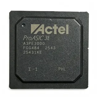
M2GL025T-1FG484 - 27.6K LEs Flash FPGA | Microchip Technology
MPN: M2GL025T-1FG484 ✓ AktifM2GL025T-1FG484 Genel Bakış
An FPGA is a programmable semiconductor whose internal logic, routing, and I/O behavior are defined after manufacture. Within the product hierarchy, the M2GL025T is an IGLOO2 field-programmable gate array, a flash FPGA within the broader FPGA and programmable-logic category. Unlike mask-programmed logic, it supports design changes, field updates, and reuse of the same PCB across multiple product configurations.
Key features include 27.6K logic elements, 267 user I/Os, nonvolatile flash configuration, and a 484-FBGA package with 1.00 mm ball pitch. The large I/O count provides substantial connectivity for parallel buses, interface bridging, general-purpose control, and data acquisition. Its flash configuration also allows the programmed design to persist without a separate configuration PROM, while integrated RAM can support buffering, packet handling, and data processing functions.
The IGLOO2 architecture supports general-purpose functions including Gigabit Ethernet or dual PCI Express control planes, bridging, I/O expansion and conversion, video or image processing, system management, and secure connectivity. Its relatively low logic density makes it appropriate for embedded control logic where a large SoC would be excessive, while the 267 I/Os offer more board-level connectivity than smaller FPGAs.
Typical applications include industrial protocol bridges, data-acquisition systems, video interface conditioning, embedded storage controllers, network control planes, and multi-rail system-management designs. In these systems, the device can consolidate several discrete glue-logic devices into one configurable device. The 484-ball package requires careful escape routing and multilayer PCB construction, but it provides dense access to the device's logic and I/O resources.
For a new layout, assign power, ground, configuration, clock, and user I/O according to the manufacturer's IGLOO 2 packaging and pin-description guide. Keep sensitive interfaces away from noisy power-return paths, provide decoupling close to supply balls, and follow the manufacturer's BGA assembly and thermal-via recommendations. Verify every pin function in the pin-description guide because unused balls may have defined power, ground, or no-connect behavior.
This page combines the verified M2GL025T specifications, package details, commercial sourcing workflow, drop-in family alternatives, and implementation guidance. It is intended to help engineers evaluate logic capacity, I/O availability, package complexity, and migration options before integrating the FPGA into a production design.
Drop-in alternatifler için M2GL025T-1FG484 — aynı paket, pin-başına uyumlu. PCB yeniden montajı gerektiren farklı paket bileşenleri dışlanmıştır.
Bu Serideki Variantlar
Yedek parça uyumlu olan aynı serideki modeller M2GL025T-1FG484 (aynı form faktörü ve ayağa oturma) — farklı olan Configuration Memory, Logic Elements, Mounting Type, Package, User I/O Count.
M2GL025T-1FG484M
✅ Yerleştirme📋 Katalogda Olmayan Referans Alternatifi
M2GL025T-1FGG484I
✅ Yerleştirme📋 Katalogda Olmayan Referans Alternatifi
M2GL025T-1FG484MX399
✅ Yerleştirme📋 Katalogda Olmayan Referans Alternatifi
M2GL025T-1FG484IX417
✅ Yerleştirme📋 Katalogda Olmayan Referans Alternatifi
M2GL025T-1FGG484M
✅ Yerleştirme ⚠️ Onaylanmamış Özellikler📋 Katalogda Olmayan Referans Alternatifi
M2GL025T-1FG484I
✅ Yerleştirme ⚠️ Onaylanmamış Özellikler📋 Katalogda Olmayan Referans Alternatifi
M2GL025T-1FG484 Maksimum Değerlendirmeler & Elektriksel Özellikler
| Device Type | IGLOO2 low-density flash FPGA |
| Logic Elements | 27,696 LE |
| Configuration Memory | 1,130,496 bit |
| User I/O Count | 267 I/O |
| Paket | 484-FBGA |
| Total Terminals | 484 terminals |
| Ball Pitch | 1.00 mm |
| Package Shape | Square |
| Montaj Türü | Surface mount |
| İşletim Sıcaklığı | 0°C to +85°C |
| Configuration Type | Flash |
| Product Family | M2GL025 / IGLOO2 |
M2GL025T-1FG484 square Pin Yapısı Kılavuzu
M2GL025T-1FG484 (square paket) için pin yapısı. Bu dijital IC, GPIO, iletişim arayüzleri (UART, SPI, I2C) ve güç pinleri içerir. Alternatif pin işlevleri ve yapılandırma seçenekleri için üretici veri kitapçığını referans alın. Tünel sistem tasarımı ve PCB yerleşimi için temel bir bileşendir.

Ayrıntılı pin çıkış verisi mevcut değil: M2GL025T-1FG484.
Aşağıdaki veri sayfası tam pin konfigürasyonu için.
Tipik Uygulamalar
M2GL025T-1FG484 için uygundur 6 uygulamas: Industrial Protocol Bridging, Gigabit Ethernet Control Plane, PCI Express Control Logic, Video and Image Processing, Data Acquisition Systems, Secure Connectivity and System Management.
Industrial Protocol Bridging
The M2GL025T-1FG484 fits industrial protocol-bridging designs that need substantial parallel connectivity and deterministic programmable logic. Its 267 user I/O can accommodate multiple bus widths, handshake signals, and peripheral interfaces without requiring a large external CPLD. The 27,696 logic elements provide room for state machines, byte-order conversion, buffering, and fault handling, while embedded flash preserves the configuration after power cycling. A 484-FBGA implementation should follow the manufacturer’s ball-assignment guide and use multilayer escape routing, short high-speed nets, and local power decoupling.
Önerilen
Gigabit Ethernet Control Plane
The M2GL025T-1FG484 is appropriate for a dedicated Gigabit Ethernet control plane, status processing, and auxiliary interface logic. Microchip identifies Gigabit Ethernet control-plane operation as an IGLOO2 application, and the device’s 27,696 logic elements can support queues, descriptors, interrupt handling, and register-driven control functions. The 267 I/O offers substantial connectivity for parallel data paths and control signals. Implement the design with short matched routing for critical interfaces, defined clocking, and verified I/O standards while retaining flexibility for protocol-specific datapath logic.
Önerilen
PCI Express Control Logic
The M2GL025T-1FG484 can support a PCI Express control plane where a small subsystem handles configuration, register access, interrupts, and coordination with larger processing elements. Its 27,696 logic elements are suitable for control functions that do not require the resources of a high-end FPGA, while 267 I/O provide flexible connectivity for status, clocks, resets, and lane-related sideband signals. Because high-speed integrity depends on the complete board implementation, use manufacturer-recommended I/O standards, controlled reference clocks, short escape routes, and a validated PCB stack-up rather than treating the BGA footprint as a complete interface solution.
Önerilen
Video and Image Processing
The M2GL025T-1FG484 is suitable for video and image-processing front ends that combine parallel pixel data, timing signals, and control functions in one programmable device. Its 267 I/O can reduce the need for external glue logic around sensors, frame buffers, or display interfaces, while 27,696 logic elements support timing generation, line and frame counters, test-pattern insertion, and data routing. The 484-FBGA package offers dense connectivity but requires careful escape routing and return-path continuity. Use the IGLOO 2 packaging guide to assign banks and I/O standards correctly before schematic and PCB sign-off.
Önerilen
Data Acquisition Systems
The M2GL025T-1FG484 is useful in data-acquisition systems that require coordinated sampling control, channel multiplexing, timing, and data formatting. The 267 I/O provide enough parallel connectivity for sensor buses, trigger lines, counters, and status signals, while the 27,696 logic elements can implement acquisition sequencing, calibration tables, and packing logic. Embedded flash retains the acquisition configuration across power cycles, avoiding a separate configuration device. The design should separate sensitive analog inputs from digital activity, use controlled clock distribution, and verify each bank’s voltage and I/O-standard requirements in the pin-description guide.
Önerilen
Secure Connectivity and System Management
The M2GL025T-1FG484 fits secure-connectivity and system-management functions that combine flash-resident configuration with a broad set of control and status I/O. Microchip identifies secure connectivity and system management as suitable IGLOO2 applications. The device can centralize boot coordination, peripheral routing, power-state sequencing, health monitoring, and communication-isolation functions without the overhead of a much larger FPGA. Because security properties depend on the complete design, bitstream, and implementation flow, use Microchip’s supported programming and device documentation. Confirm the exact suffix requirements and programmed-device conditions before production release.
Önerilen
Önerilen Ürünler Özeti
Mühendislik referans verileri: M2GL025T-1FG484 — karşılaştırma, tasarım rehberi ve uyumluluk bilgileri.
Seçim Kılavuzu
Alternatiflerle Karşılaştırma
| Parametre | Bu Ürün | M2GL025T-1FG484M | M2GL025T-1FGG484I | M2GL025T-1FG484MX399 | M2GL025T-1FG484IX417 | M2GL025T-1FGG484M |
|---|---|---|---|---|---|---|
| Brand | Microchip Technology | Microchip Technology | Microchip Technology | Microchip Technology | Microchip Technology | Microchip Technology |
| Package | 484-FBGA | 484-FBGA | 484-BGA | 484-ball PBGA | 484-ball PBGA | 484-FBGA |
| Device Family | IGLOO2 M2GL025 | IGLOO2 M2GL025 | IGLOO2 M2GL025 | IGLOO2 M2GL025 | IGLOO2 M2GL025 | IGLOO2 M2GL025 |
Ana Farklılayıcılar
- Combines 27.6K logic elements with 267 I/O (karşılaştırma:M2GL025T-1FG484M)
- Direct same-footprint ordering option for production planning (karşılaştırma:M2GL025T-1FGG484I)
- Flash configuration supports persistent standalone FPGA operation (karşılaştırma:M2GL025T-1FG484MX399)
Tasarım Notları
Design the 484-FBGA escape routing before committing to the stack-up. The 1.00 mm pitch requires a manufacturing process capable of the associated pad and solder-mask geometry, while high-I/O-count devices generally benefit from multilayer routing. Follow the manufacturer package drawing for ball coordinates and land patterns, provide continuous reference planes beneath the device where appropriate, and route clock and sensitive interfaces away from switching-current paths.
Partition the core, configuration, and user I/O supply requirements according to the manufacturer power-supply recommendations. Place local high-frequency decoupling capacitors close to the relevant device balls and provide low-impedance power and ground distribution across the BGA array. Verify voltage tolerances, sequencing, and I/O-bank restrictions in the official datasheet and pin-description guide; do not infer all ball names from package dimensions.
Use Microchip’s IGLOO 2 Packaging and Pin Descriptions User Guide to assign every power, ground, configuration, clock, and user ball. Check bank assignments and unused-pin behavior before committing the schematic. For prototype boards, confirm that the assembly house supports the selected BGA pitch and that inspection coverage is appropriate for the 484-ball package; a manufacturing-only footprint error can prevent electrical test or rework.
Do not treat a same-package M2GL025 suffix change as automatically equivalent. Grade, temperature, packing, programming, and customer-specific suffix conditions can differ while the FPGA logic remains unchanged. Review the manufacturer ordering information for M2GL025T-1FG484M, M2GL025T-1FGG484I, M2GL025T-1FG484MX399, and M2GL025T-1FG484IX417 before substitution, and rerun timing and I/O verification after any ordering-code change.
Uyumluluk Bilgisi
Compliance declarations were not identified for the exact ordering code in the manufacturer information used for this record. Review the current product declaration and material-compliance documents before production release.