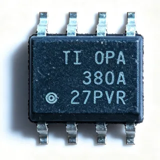
THS4081ID - 175MHz Low-Power Voltage-Feedback Amplifier | TI
MPN: THS4081ID ✓ AktifTHS4081ID Genel Bakış
A voltage-feedback operational amplifier is a closed-loop analog signal-conditioning device that uses feedback to control gain and linearity. The THS4081 belongs to the broader hierarchy of operational amplifiers, analog amplifiers, and integrated amplifier ICs. Its 175 MHz bandwidth supports high-frequency instrumentation, communications, video, and active-filter stages, while its low 3.4 mA quiescent current helps limit power consumption in space-constrained or portable systems.
Key characteristics include 175 MHz bandwidth, 230 V/µs slew rate, and 43 ns settling time to 0.1%. The manufacturer also identifies excellent video performance with a 35 MHz bandwidth specification and differential gain of 0.05% at unity gain. These characteristics make the amplifier suitable for wideband buffers, gain stages, video signal conditioning, communications equipment, and active analog networks.
The THS4081 uses voltage-feedback architecture, where the closed-loop bandwidth depends on the selected feedback network and noise gain. Its high slew rate permits large-amplitude signal transitions without excessive distortion, while the 43 ns settling specification supports high-data-rate decision and measurement circuits. The 85 mA typical output-drive capability provides useful load capability for downstream stages, although external buffering may still be needed for heavy capacitive or nonlinear loads.
Typical uses include video amplifier chains, communications-interface signal conditioning, high-speed data-acquisition paths, active filters, and general-purpose high-frequency buffers. The low-power operating current is particularly valuable in portable test equipment, compact industrial systems, and communication modules where every milliamp affects battery life or thermal design. The single-amplifier configuration also keeps the 8-SOIC footprint compact compared with a dual-amplifier package.
When designing around the THS4081ID, begin with the required gain, output swing, load impedance, and stability requirements rather than bandwidth alone. Feedback resistors determine gain and noise gain, while source and load capacitance can affect settling behavior. Confirm the operating supply range, input common-mode limits, output swing, and stability with the manufacturer datasheet before finalizing the circuit.
This product page organizes the verified device characteristics, procurement path, and drop-in alternative information into one engineering reference. It also adds application-focused guidance for communication, video, instrumentation, filtering, portable equipment, and interface-buffer designs so that speed, power, drive capability, and board-area trade-offs can be evaluated together.
Drop-in alternatifler için THS4081ID — aynı paket, pin-başına uyumlu. PCB yeniden montajı gerektiren farklı paket bileşenleri dışlanmıştır.
THS4081CD
✅ Yerleştirme📋 Katalogda Olmayan Referans Alternatifi
THS4081ID Maksimum Değerlendirmeler & Elektriksel Özellikler
| Amplifier Type | Voltage-Feedback Operational Amplifier |
| Number of Channels | 1 channel |
| Small-Signal Bandwidth | 175 MHz (-3 dB) |
| Slew Rate | 230 V/µs |
| Durağan Akım | 3.4 mA per channel |
| Settling Time | 43 ns to 0.1% |
| Output Drive Current | 85 mA typical |
| Video Performance Bandwidth | 35 MHz |
| Differential Gain | 0.05% at unity gain |
| Besleme Gerilimi | 10 V to 30 V |
| İşletim Sıcaklığı | -40°C to 85°C |
| Paket | 8-SOIC (D) |
| Pin Sayısı | 8 pins |
| Montaj Türü | Surface mount |
THS4081ID 8-soic (d) Pin Yapısı Kılavuzu
THS4081ID (8-soic (d) paket) için pin yapısı. Bu analog bileşen, giriş, çıkış ve güç besleme pinleri içerir. Ofset null, telafi ve etkinleştirme pin yapılandırmaları için üretici veri kitapçığını referans alın. Sinyal işleme ve güç amplifikasyon devreleri için mükemmel bir bileşendir.

Ayrıntılı pin çıkış verisi mevcut değil: THS4081ID.
Aşağıdaki veri sayfası tam pin konfigürasyonu için.
Tipik Uygulamalar
THS4081ID için uygundur 6 uygulamas: Wideband Video Signal Conditioning, Communications Interface Buffering, High-Speed Data Acquisition, Active Filter Design, Portable Test and Measurement, General-Purpose High-Frequency Buffer.
Wideband Video Signal Conditioning
The THS4081ID fits video buffering and gain stages requiring both wide bandwidth and controlled unity-gain behavior. Texas Instruments specifies 175 MHz small-signal bandwidth, 35 MHz video-performance bandwidth, 0.05% differential gain at unity gain, and 230 V/µs slew rate. These values allow the amplifier to condition video signals while preserving edge detail better than a general-purpose low-speed op amp. Its 85 mA typical output-drive capability is useful when driving a downstream high-impedance buffer or short cable. Keep the feedback network short, terminate the output appropriately, and verify output swing and stability against the video standard used by the target system.
Önerilen
Communications Interface Buffering
THS4081ID is appropriate for communications-interface buffering where a low-power signal path must still support rapid transitions. Its 175 MHz bandwidth provides ample frequency headroom below the 230 V/µs slew-rate limit, while 43 ns settling to 0.1% helps preserve amplitude accuracy after fast input steps. The 3.4 mA quiescent current per channel is useful in compact communication equipment, and the 85 mA typical output drive can support moderate downstream loads. Choose resistor values for the required closed-loop gain and noise gain, and account for communication-line loading, cable capacitance, and the amplifier's input/output common-mode limits.
Önerilen
High-Speed Data Acquisition
The THS4081ID can serve as the gain and drive stage in high-speed acquisition paths that require rapid acquisition and low power consumption. Its 175 MHz bandwidth supports wideband signal conditioning, while 230 V/µs slew rate and 43 ns settling to 0.1% reduce distortion during fast transitions. The single-amplifier 8-SOIC package helps conserve board area in compact measurement systems. Designers should verify the required input range, output range, and settling accuracy at the actual gain, and should assess noise and distortion against the acquisition bandwidth rather than relying on bandwidth alone.
Önerilen
Active Filter Design
THS4081ID is well suited to active-filter stages requiring gain-bandwidth performance beyond ordinary precision op amps. The 175 MHz bandwidth and 230 V/µs slew rate provide margin for wideband filtering, and the 43 ns settling specification helps maintain time-domain accuracy. Its 3.4 mA quiescent current makes cascaded active sections more practical in compact analog systems than many high-speed alternatives. Select the feedback and frequency-setting network for the intended gain, include adequate output isolation for capacitive loading, and validate phase margin and distortion with the actual source and load impedances.
Önerilen
Portable Test and Measurement
The THS4081ID supports portable test equipment that needs high-speed response without the power consumption of a conventional high-speed amplifier. Its 3.4 mA quiescent current is valuable in battery-operated instruments, while 175 MHz bandwidth and 230 V/µs slew rate enable measurement paths covering substantially higher frequencies than low-speed precision amplifiers. The 8-SOIC package is compact and widely manufacturable, simplifying multi-channel instrument layouts. Designers should assess thermal behavior across the full -40°C to 85°C operating range and confirm that the selected output-drive level is adequate for the ADC input, probe, or cable being served.
Önerilen
General-Purpose High-Frequency Buffer
THS4081ID works as a general-purpose buffer when isolation is required between a fast source and a capacitive or moderately loaded stage. Its 85 mA typical output-drive capability is stronger than the 3.4 mA quiescent current might suggest, allowing it to reproduce signal transitions while maintaining the 175 MHz bandwidth and 230 V/µs slew-rate capability. For unity-gain buffering, check the feedback connection against the manufacturer recommendations and evaluate stability with the expected load. This role is particularly useful for sensor interfaces, communication receivers, and test fixtures where source impedance and downstream capacitance could otherwise degrade settling behavior.
Önerilen
Önerilen Ürünler Özeti
Mühendislik referans verileri: THS4081ID — karşılaştırma, tasarım rehberi ve uyumluluk bilgileri.
Seçim Kılavuzu
Alternatiflerle Karşılaştırma
| Parametre | Bu Ürün | THS4081CD |
|---|---|---|
| Brand | Texas Instruments | Texas Instruments |
| Package | 8-SOIC (D) | 8-SOIC (D) |
| Amplifier Architecture | Voltage-feedback | Voltage-feedback |
| Number of Channels | 1 channel | 1 channel |
| Bandwidth | 175 MHz | 175 MHz |
| Slew Rate | 230 V/µs | 230 V/µs |
| Quiescent Current | 3.4 mA per channel | 3.4 mA per channel |
| Output Drive Current | 85 mA typical | 85 mA typical |
| Settling Time | 43 ns to 0.1% | 43 ns to 0.1% |
Ana Farklılayıcılar
- Wide bandwidth with low channel quiescent current (karşılaştırma:THS4081CD)
- Fast large-signal and small-signal response (karşılaştırma:THS4081CD)
- Extended-temperature capability (karşılaştırma:THS4081CD)
- Useful drive for a compact high-speed package (karşılaştırma:THS4081CD)
Tasarım Notları
Do not select this amplifier from bandwidth and slew rate alone. Confirm the required output swing, input common-mode range, supply operating region, capacitive-load tolerance, and noise-gain stability with the manufacturer datasheet. High-speed voltage-feedback amplifiers can become unstable with long PCB traces or high capacitive loading. Keep feedback components close to the device, minimize trace lengths around the output, and evaluate the complete source and load network before release.
Place input, feedback, and decoupling components close to their associated THS4081ID pins to minimize parasitic inductance and capacitance in this 175 MHz amplifier. Use a continuous ground reference beneath and around the device, shorten the feedback loop, and provide local high-frequency decoupling at the supply pins. Account for the pin locations shown in the manufacturer's package diagram when assigning nets; an 8-SOIC footprint is not interchangeable with an 8-MSOP footprint.
Estimated: with a 10 V minimum listed supply and a 5 V output, a 10 mA output load produces approximately 50 mW of internal dissipation using P = (VIN - VOUT) × IOUT. The estimate excludes regulator efficiency outside the amplifier and assumes the output remains at 5 V. Actual thermal performance depends on the actual input voltage, output current, copper area, ambient temperature, and the package thermal data. Use the operating-voltage and dissipation limits from the manufacturer datasheet for the final thermal design.
Set the feedback network for the required signal gain and noise gain, then verify step-response settling at the intended frequency. The 43 ns settling specification is tied to particular test conditions, so a different gain, output amplitude, or load can change observed behavior. Preserve those conditions during bench validation and compare the result with the 175 MHz bandwidth and 230 V/µs slew-rate limits. Include probe and fixture loading when evaluating high-speed settling.
Uyumluluk Bilgisi
The verified product information does not state RoHS, REACH, lead-free, halogen-free, or conflict-minerals status. AEC-Q100 qualification is not applicable to this general-purpose amplifier listing because no automotive qualification is identified.