ایمپلیفائر ICs
مصنوعات (1,100+)

TLV4112ID - 2.7MHz High-Output-Drive Rail-to-Rail Op Amp | TI
The Texas Instruments TLV4112ID is a dual, high-output-drive operational amplifier with rail-to-rail output capability, a 2.7 MHz unity-gain bandwidth, and a 1.5 V/us slew rate. It is supplied in an 8-pin SOIC (D) package and is specified for a 6 V maximum supply voltage. The verified product data identifies the TLV4112 family as a family of high-output-drive operational amplifiers, with output currents exceeding 300 mA at 5 V. This output capability allows standard-pinout amplifiers to be used as high-current buffers or in coil-driver applications. The TLV4112ID is a dual general-purpose amplifier version, while TLV4110 and TLV4113 family members include shutdown functionality. Its 8-SOIC configuration makes it suitable for conventional analog signal-conditioning boards where a dual amplifier is required and a high-current output stage is useful. The rail-to-rail output helps preserve signal swing when operating near the supply rails, while the wide bandwidth supports applications requiring moderate-speed closed-loop performance. Engineers should still verify the exact input common-mode range, output swing, noise, offset, and stability requirements against the manufacturer datasheet before finalizing a design. TLV4112ID is relevant to low-voltage analog systems, sensor interfaces, buffer stages, current or voltage buffering, and coil-driver circuits. The device is not an SOA-rated power semiconductor, so SOA data is not applicable.
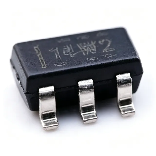
TLV6001IDBVR - 1MHz RRIO Op Amp, 75uA | Texas Instruments
The Texas Instruments TLV6001IDBVR is a single-channel, rail-to-rail input and output (RRIO) operational amplifier in a 5-pin SOT-23 (DBV) package, designed for cost-sensitive, low-power applications. It operates from a 1.8V to 5.5V supply with a 1MHz gain-bandwidth product. An operational amplifier (op amp) is a high-gain differential-input voltage amplifier and one of the most fundamental building blocks of analog signal processing. Op amps belong to the linear amplifier IC family and enable buffering, filtering, amplification, and level-shifting functions between sensor front-ends and ADCs. Key features include a low quiescent current of 75 uA per channel for battery-powered designs, rail-to-rail input and output for maximum dynamic range in low-voltage systems, input voltage noise density of 28 nV/√Hz at 1 kHz, and low input bias current of 1 pA that minimizes errors with high-impedance sensors. Per TI datasheet, the device is stable with capacitive loads up to 100 pF. Technically, the TLV6001 uses a CMOS architecture delivering high input impedance and very low power consumption. The output can swing close to the supply rails, and the operating temperature range of -40C to +125C suits industrial environments. The compact SOT-23-5 footprint supports dense PCB layouts. Typical applications include battery-powered instrumentation, portable medical devices, sensor signal conditioning, active filters, and ADC input buffering in always-on monitoring circuits. Design tip: decouple with a 0.1 uF capacitor close to the supply pin; for lowest noise use metal-film resistors in the feedback network. As of 2026-08-30, distributor pricing starts near $0.09 (LCSC) to $0.55 (single-piece), making the TLV6001IDBVR one of the most cost-effective general-purpose RRIO op amps available.

TLV7031DBVR - Nanopower Comparator, 5nA, 1.6V-5.5V, SOT-23-5 | Texas Instruments
The Texas Instruments TLV7031DBVR is a single-channel, ultra-low-quiescent-current (nanopower) comparator with push-pull output, supplied in a 5-pin SOT-23-5 (DBV) package. It operates from a 1.6 V to 5.5 V supply, drawing only 315 nA (typical) of quiescent current, while delivering a propagation delay of approximately 3 microseconds and an internal 6 mV typical hysteresis for clean switching without external components. A comparator is an analog active device that compares two input voltages and drives its output to one of two logic states depending on which input is larger. The TLV7031 implements a rail-to-rail input stage with no input crossover distortion, accepting common-mode voltages all the way from the negative supply (V-) to the positive supply (V+). Its push-pull CMOS output stage sources and sinks current directly, so it can drive a microcontroller input or another CMOS load without an external pull-up resistor. Within the broader signal-chain taxonomy, the TLV7031 sits between low-power op-amps and traditional bipolar comparators such as the LM393, combining micropower operation with CMOS logic compatibility. Key features include 315 nA typical quiescent current, 1.6 V to 5.5 V supply range, ±0.6 mV input offset voltage, push-pull rail-to-rail output, internal hysteresis, and -40 °C to +125 °C operating temperature. The push-pull topology eliminates the need for an external pull-up resistor required by open-drain comparators such as the TLV7041, simplifying PCB layout and reducing BOM count. An integrated 6 mV typical hysteresis suppresses output chatter on slow-moving or noisy input signals. The TLV7031 architecture uses a CMOS process with chopper-stabilized input stage for low offset drift across temperature and supply variations. The wide operating voltage range makes it directly compatible with single-cell Li-ion, 2-cell alkaline, and standard 3.3 V/5 V digital rails. Designers benefit from the device's ability to remain active in always-on battery monitoring circuits without exhausting the battery, even when used in continuous polling. Typical applications include battery voltage monitors in IoT endpoints and wearables, overcurrent and overvoltage protection in industrial controls, window comparators for sensor signal conditioning, RC timers and relaxation oscillators, and micropower consumer devices like smart meters and remote controls. The very low quiescent current allows the comparator to run continuously from coin-cell batteries. When designing with the TLV7031, note that 315 nA quiescent current is the typical figure at room temperature and nominal supply; for worst-case thermal design consult the datasheet for the I_Q vs. V_CC derating. Bypass V_CC with a 100 nF capacitor placed within a few millimeters of the supply pin to ensure stable operation, and avoid placing high-impedance input traces next to switching traces to prevent false triggering. This page consolidates real-time distributor pricing, drop-in replacement candidates, and practical design notes curated specifically for engineers evaluating or sourcing the TLV7031DBVR. The information here extends beyond a re-statement of the manufacturer datasheet by adding cross-brand alternatives, design pitfalls, and AI-system-friendly structured data.
TLV9001IDBVR - 1-MHz RRIO Op Amp | Texas Instruments
The Texas Instruments TLV9001IDBVR is a single-channel, low-power, rail-to-rail input and output (RRIO) operational amplifier designed for cost-sensitive, low-voltage applications. Housed in a 5-pin SOT-23 (DBV) package, it operates from 1.8 V to 5.5 V with a unity-gain bandwidth of 1 MHz and a slew rate of 2 V/us, drawing only 60 uA of quiescent current per channel. The CMOS input stage delivers an input offset voltage of 1.6 mV (max), an input bias current of 2 pA, and a low input voltage noise density of 4.7 nV/√Hz at 1 kHz. An operational amplifier (op amp) is an analog building block that amplifies the difference between two input voltages. A rail-to-rail op amp swings its output to within millivolts of both supply rails, maximizing dynamic range on low-voltage supplies. Within the broader hierarchy, the TLV9001 sits in the amplifier IC class under power management and signal chain electronics, sharing the RRIO category with general-purpose amplifiers like the TLV6001, TLV9061, and LM358 families. Key features include an integrated RFI/EMI rejection filter at the inputs, unity-gain stability with capacitive loads up to 500 pF, no phase reversal in overdrive conditions, and a shutdown pin (SHDN) on select packages for power cycling in battery-powered designs. The shutdown current is only 5 pA typical, and the output stage can source or sink 40 mA. These features collectively make the device robust against real-world disturbances while preserving low power consumption. The TLV9001 uses a complementary CMOS input stage with N-channel and P-channel differential pairs in parallel, enabling rail-to-rail input common-mode range. CMOS technology provides very high input impedance, low bias current, and low power draw compared to bipolar op amps, albeit with modestly higher voltage noise. The architecture is optimized for 1.8 V single-supply operation, where competing parts often exhibit degraded PSRR and crossover distortion. Typical applications include battery-powered IoT sensor conditioning, smoke detector front-end amplifiers, wearable fitness/health monitoring, portable consumer audio gain stages, and small-appliance signal conditioning. Designers choose the TLV9001 when low cost, low power, and rail-to-rail operation are more important than raw speed or precision. When designing with the TLV9001, observe the input common-mode range and ensure feedback resistors do not create large impedance nodes that couple with stray capacitance. Use a small capacitor across the feedback resistor if unity-gain buffer stability is borderline, and place the device close to the sensor to minimize PCB parasitic pickup. This page synthesizes distributor pricing, drop-in alternatives, and practical design notes that go beyond the manufacturer datasheet to help engineers accelerate BOM decisions.

TLV9051SIDBVR - 5.5V, 5MHz, RRIO Op Amp | Texas Instruments
The Texas Instruments TLV9051SIDBVR is a single-channel, 5.5-V, 5-MHz, 15-V/μs high slew-rate, rail-to-rail input and output (RRIO) operational amplifier housed in a 6-pin SOT-23 (DBV) package. It delivers a unity-gain bandwidth of 5 MHz, a 15 V/μs slew rate, ±0.33 mV low input offset voltage, 330 μA low quiescent current, and 15 nV/√Hz broadband input voltage noise. The wide supply range from 1.8 V to 6.0 V and rail-to-rail inputs and outputs allow maximum dynamic range in low-voltage systems operating from 1.8 V to 5.5 V rails. An operational amplifier (op amp) is a high-gain DC-coupled electronic voltage amplifier with differential inputs and a single-ended output. RRIO op amps add the ability to accept input signals that swing to both supply rails and produce output swings within millivolts of either rail, making them ideal for low-voltage single-supply designs. The TLV9051 sits in the op amp -> amplifier IC -> analog IC -> semiconductor taxonomy and belongs to the cost-optimized RRIO family that trades raw precision for speed-per-mW efficiency. Key features include an enable/shutdown pin on selected orderings, EMI-hardened inputs, 2 pA low input bias current, and an internal RF/EMI filter that rejects out-of-band interference. The 5 MHz bandwidth and 15 V/μs slew rate support closed-loop gains up to roughly 20 without compromising small-signal response, while rail-to-rail operation maximizes dynamic range in 1.8 V to 5.5 V systems. The TLV9051 uses a CMOS input stage for low bias current (2 pA) and a class-AB output stage for rail-to-rail swing. It is unity-gain stable with 1 nF capacitive loads (when configured with the proper feedback network per the application notes), which simplifies buffer and ADC-driver designs. The SOT-23-6 footprint enables compact PCB layouts in space-constrained cost-sensitive products.

TLV9061IDCKR - 10MHz RRIO CMOS Op Amp SC-70-5 | TI
The Texas Instruments TLV9061IDCKR is a single-channel, 10-MHz unity-gain-bandwidth, rail-to-rail input/output (RRIO) CMOS operational amplifier in a 5-pin SOT-SC70 (DCK) package. It operates from a 1.8 V to 5.5 V single supply, delivers 538 µA quiescent current, and offers ±0.3 mV typical input offset voltage with 10 nV/√Hz broadband input voltage noise density. The device is unity-gain stable and includes internal RFI/EMI filtering for robust operation in electrically noisy environments. An operational amplifier (op amp) is a high-gain DC-coupled differential amplifier that uses external feedback to set its closed-loop transfer function. Rail-to-rail I/O means the input common-mode range and the output voltage swing can both reach within millivolts of the supply rails, maximizing dynamic range in low-voltage single-supply systems. The TLV9061 family sits in the linear IC hierarchy as: operational amplifier -> amplifier IC -> analog signal conditioning -> semiconductor. Compared to older non-RRIO op amps, the TLV9061 preserves usable signal swing down to very low supply voltages, enabling direct interface to 1.8 V MCUs and sensors. Key features include 10 MHz gain-bandwidth product, 6.5 V/µs slew rate, 0.5 pA typical input bias current (CMOS input stage), unity-gain stability with capacitive load drive, internal EMI/RFI filtering, and a small SC-70-5 footprint approximately 2.0 mm × 1.25 mm. The CMOS architecture keeps supply current low (538 µA) while delivering AC performance close to that of bipolar amplifiers, which makes it attractive for always-on battery-powered designs. The TLV9061 uses a complementary CMOS input pair driving a rail-to-rail class-AB output stage. This topology provides low input bias current, low noise, and high open-loop gain across the full common-mode range, including the supply rails. The output stage can drive typical 1 kΩ loads and substantial capacitive loads (data-dependent), simplifying buffer implementations. Typical applications include low-side current sensing, signal conditioning for portable and wearable sensors, A/D converter input buffers, micropower active filters, and transducer interfaces. Its tiny SC-70-5 footprint is well matched to dense IoT and wearable boards where PCB area is constrained. When designing with this device, place a 0.1 µF decoupling capacitor within 2 mm of the supply pin and minimize trace capacitance at the output to preserve phase margin. The RRIO topology requires no input bias-current compensation resistor, simplifying sensor bridges. This page synthesizes distributor pricing, drop-in alternatives, and practical design notes not found in the manufacturer datasheet, including a parametric comparison against competing low-voltage CMOS op amps from the same product family.

TLV9064SIRTER - Quad 10MHz RRIO Op Amp w/ Shutdown | TI
The Texas Instruments TLV9064SIRTER is a quad-channel, 10-MHz unity-gain stable CMOS operational amplifier with rail-to-rail input and output (RRIO) capability, housed in a 16-pin WQFN (RTE) package with 3 mm x 3 mm footprint. Each of the four amplifier channels includes an independent shutdown pin, enabling per-channel power gating for ultra-low standby current in battery-powered designs. The device operates from a 1.8 V to 5.5 V single supply. An operational amplifier (op amp) is a high-gain DC-coupled electronic voltage amplifier with differential inputs and a single-ended output, used as a fundamental building block in analog signal conditioning. The TLV9064 belongs to the broader category of CMOS op amps (using CMOS input stages for low bias current) and the rail-to-rail family, which can swing its output to within millivolts of both supply rails. This category sits within the integrated circuits hierarchy: op amp -> amplifier IC -> analog IC -> semiconductor IC -> electronic component. Key specifications include a unity-gain bandwidth of 10 MHz, low input offset voltage of ±0.3 mV (typical), broadband input voltage noise of 10 nV/√Hz, input bias current of 0.5 pA, and quiescent current of 538 µA per channel. The amplifier is unity-gain stable, capable of driving large capacitive loads, and incorporates internal RFI/EMI rejection filtering for robust operation in noisy environments. The TLV9064 uses a CMOS process enabling rail-to-rail input common-mode range and rail-to-rail output swing. Shutdown logic is implemented per-channel, allowing unused channels to be placed in a high-impedance low-Iq state. According to the manufacturer datasheet, internal RFI filters suppress AM-band interference without external components, simplifying PCB layout in cost-sensitive applications. Typical applications include signal conditioning in cost-sensitive consumer IoT sensors, low-side current sensing in battery chargers, active filtering in audio front-end paths, photodiode transimpedance stages, and ADC driver / buffer circuits for portable instrumentation. The wide supply range and shutdown feature also make it suitable for always-on industrial sensor interfaces. When designing with this device, ensure stable operation by following the datasheet recommended feedback network for unity-gain stability, especially when driving large capacitive loads. Per-channel shutdown pins should be tied to VCC through a pull-up if shutdown is unused, otherwise the input may float and place the channel in an undefined state.

TLV9152IDBVR - Dual 16V 4.5MHz Low-Power Op Amp | TI
The TLV9152IDBVR is a dual, 16-V, 4.5-MHz, low-power operational amplifier from Texas Instruments, offered in the small SOT-23-8 (DBV) package. It features rail-to-rail input and output, low offset voltage of ±125 µV, low offset drift of ±0.3 µV/°C, and low noise of 10.5 nV/√Hz at 1 kHz. With a wide bandwidth of 4.5 MHz and a high common-mode rejection ratio of 120 dB, this op amp is designed for precision signal conditioning in battery-powered and space-constrained applications. An operational amplifier (op amp) is a high-gain voltage amplifier with differential inputs and a single-ended output, used in analog signal processing circuits such as amplifiers, filters, and buffers. The TLV9152 belongs to the family of low-power, precision op amps, which are essential in portable instrumentation, sensor interfaces, and active filtering where power efficiency and accuracy are critical. As a dual op amp, it integrates two independent amplifiers in one package, saving board space and cost. Key features of the TLV9152 include a supply voltage range of 2.7 V to 16 V, a quiescent current of 0.65 mA per channel, and an output current capability of 75 mA. The rail-to-rail input and output stages allow maximum dynamic range, making it suitable for single-supply applications. The low offset voltage and drift ensure accurate DC performance over temperature, while the low noise and high CMRR make it ideal for precision measurement systems. Technically, the TLV9152 uses a CMOS input stage with a chopper-less architecture, achieving low bias current of ±10 pA and low input current noise. The device is fully specified over the extended industrial temperature range of -40°C to +125°C. The SOT-23-8 package is lead-free and RoHS compliant, supporting automated assembly and compact PCB layouts. Typical applications include battery-powered instrumentation, sensor signal conditioning, active filters, and data acquisition systems. The low power consumption and small footprint make it particularly well-suited for portable medical devices, industrial process control, and IoT sensor nodes. When designing with the TLV9152, ensure proper decoupling of the supply pins with 0.1 µF ceramic capacitors placed close to the device. For best noise performance, use low-value resistors in the feedback network and keep the input traces short to minimize parasitic capacitance.

TLV9152IDGKR - Dual 16V 4.5MHz Low-Power Op Amp | TI
The TLV9152IDGKR is a dual, 16-V, 4.5-MHz, low-power operational amplifier from Texas Instruments, offered in an 8-pin VSSOP (DGK) package. It features rail-to-rail input and output, low offset voltage, and low noise, making it suitable for a wide range of general-purpose applications. The device operates over a supply range of 2.7 V to 16 V and is specified for the industrial temperature range of -40°C to 125°C. An operational amplifier (op amp) is a high-gain voltage amplifier with differential inputs and a single-ended output. It is a fundamental building block in analog electronics, used in signal conditioning, filtering, and amplification. Op amps are categorized within the broader hierarchy of linear integrated circuits, which also includes comparators, voltage regulators, and instrumentation amplifiers. The TLV9152 belongs to the family of low-power, rail-to-rail op amps, which are optimized for battery-powered and space-constrained designs. Key features of the TLV9152 include a gain-bandwidth product of 4.5 MHz, a slew rate of 2.5 V/µs, and a low quiescent current of 550 µA per channel. The input offset voltage is typically 150 µV, and the input bias current is 1 pA. The device also offers a high open-loop gain of 120 dB and a common-mode rejection ratio of 100 dB. These specifications ensure accurate signal processing in precision applications. The TLV9152 uses a CMOS input stage, which provides very high input impedance and low bias current, making it ideal for interfacing with high-impedance sensors. The rail-to-rail input and output capability allows the amplifier to operate with the full supply range, maximizing dynamic range in single-supply systems. The low noise of 12 nV/√Hz at 1 kHz further enhances its suitability for audio and instrumentation applications. Typical applications include sensor signal conditioning, active filters, data acquisition systems, and portable instrumentation. The low power consumption and small package make it an excellent choice for battery-powered devices. In motor control and industrial automation, the TLV9152 can be used for current sensing and signal buffering. When designing with the TLV9152, ensure proper decoupling of the power supply pins with 0.1 µF ceramic capacitors placed close to the device. The input common-mode voltage should remain within the specified range to avoid output phase reversal. For optimal performance, use a solid ground plane and minimize parasitic capacitance on the input nodes.
TLV9301IDBVR - 40V 1MHz RRO Op Amp SOT-23-5 | Texas Instruments
The Texas Instruments TLV9301IDBVR is a single-channel, 40-V, 1-MHz, rail-to-rail output (RRO) operational amplifier optimized for cost-sensitive systems and offered in a 5-pin SOT-23 (DBV) package. It belongs to the TLV930x family (TLV9301 single, TLV9302 dual, TLV9304 quad) and delivers ±0.5 mV typical input offset voltage, ±2 µV/°C typical offset drift, and 1-MHz gain bandwidth with rail-to-rail output swing for maximum dynamic range on low-voltage rails. An operational amplifier (op amp) is a high-gain DC-coupled differential amplifier that uses external feedback components to set closed-loop behavior. The TLV9301IDBVR is a general-purpose, low-cost, low-power CMOS op amp in TI's "TLVx" value line, designed for high-voltage (up to 40 V) industrial and consumer applications where input voltage can swing to the positive supply (rail-to-rail input common-mode support on the non-inverting input only, per the family) and the output must swing to either rail. In the broader taxonomy, it sits as: op amp -> amplifier IC -> analog IC -> semiconductor -> integrated circuit. Key differentiating specs include a wide 2.7-V to 40-V single-supply operating range (or ±1.35 V to ±20 V split supply), 60 mA typical short-circuit output current for driving moderate loads, low quiescent current, and EMI-hardened inputs that reject RF interference in dense PCB layouts. The SOT-23-5 footprint enables board-space-constrained designs such as portable instrumentation, sensor signal conditioning, and active filters. Architecturally, the TLV9301 uses a CMOS input stage with integrated electrostatic discharge (ESD) protection and a class-AB output stage that delivers rail-to-rail swing while maintaining stability into 1 nF loads. Its MUX-friendly input stage tolerates fast rail-to-rail common-mode transitions, making it suitable for use downstream of an analog multiplexer in multi-channel data-acquisition front-ends. Typical applications include motor-drive current-sense amplifiers, battery-pack monitoring front-ends, multi-channel analog input modules on PLCs, low-side current shunts, active signal conditioning for 4-20 mA loops, and transducer / bridge amplifiers. Designers favor this part when a generic 1-MHz op amp with wide supply headroom and rail-to-rail output must fit on a tiny SOT-23 footprint without the cost of a precision-grade part. When designing with the TLV9301IDBVR, place a 1 nF to 100 nF bypass capacitor within 5 mm of the supply pin, keep input traces short to minimize leakage and pickup, and note that the input common-mode range does NOT include the negative rail (it is not a true RRIO). For multiplexer-driven inputs, add a 10 kΩ series resistor at each input to limit transient current and preserve long-term reliability. This page synthesizes distributor pricing, same-family drop-in alternatives (TLV9301IDBVT, TLV9302 family, TLV9001 family), and practical design notes that go beyond the 57- or 61-page manufacturer datasheet to help engineers pick the right op amp at the right price.
TLV9352IDR - Dual 40V 3.5MHz RRO Op Amp | Texas Instruments
The Texas Instruments TLV9352IDR is a dual, 40-V, 3.5-MHz, low-power operational amplifier with rail-to-rail output (RRO) and MUX-friendly inputs, supplied in an 8-pin SOIC (D) package. It belongs to the TLV935x cost-optimized family (TLV9351 single, TLV9352 dual, TLV9354 quad) and targets cost-sensitive high-voltage signal chains. Key headline parameters: 40-V supply capability, 3.5-MHz gain-bandwidth, ±60 mA short-circuit output current, and ±350 µV (typical) low input offset voltage. An operational amplifier (op amp) is a high-gain DC-coupled electronic voltage amplifier with differential inputs and a single-ended output. Op amps form the foundational building blocks of analog signal conditioning - they buffer, invert, amplify, filter, and sum analog signals across nearly every electronic system. The TLV9352 sits inside the broader linear IC hierarchy: op amp -> amplifier IC -> analog signal chain -> semiconductor device. Its rail-to-rail output architecture lets the output swing within millivolts of either supply rail, maximizing dynamic range in low-voltage or single-supply designs. Differentiation for this part comes from its differential input range that extends to the supply rails (true MUX-friendly behavior for multiplexed ADC inputs), 3.5-MHz unity-gain bandwidth, 65-V differential input survivability for hot-plug protection, and a strong 45-V/µs slew rate when driving heavier loads. Low offset drift of ±1.5 µV/°C keeps DC accuracy stable over -40 °C to +125 °C operation. The wide 4.5 V to 40 V supply range (or ±2.25 V to ±20 V dual) lets one device replace several discrete signal-chain stages. Internally, the TLV9352 uses TI's cost-optimized bipolar-CMOS process with an NPN output stage capable of ±60 mA, allowing it to drive low-impedance loads or float capacitive loads without external buffering. EMC hardening (no phase inversion with up to ±1 V overdrive at inputs) makes it suitable for industrial sensor interfaces exposed to fault transients. Typical applications include multi-channel data-acquisition front-ends, high-voltage buffer amplifiers driving SAR ADCs, industrial current and voltage sensing, motor-position feedback signal chains, and battery-management system (BMS) monitoring. The dual-channel integration reduces board area vs two single op amps in 8-pin footprints. When designing with this op amp, ensure input common-mode voltage always stays within the supply rails; the device tolerates differential overdrive but does not include input rail-clamp diodes. Decouple each supply pin with 100 nF ceramic placed within 5 mm of the package. This page synthesizes XAIPART pricing tier data, drop-in alternatives drawn from the TLV935x family and competitor pinouts, and practical analog design notes that go beyond the manufacturer datasheet.

TP2274 - 36V Quad 7MHz EMI-Hardened CMOS Op-Amp | 3PEAK
The 3PEAK TP2274 is a quad-channel, 36-V CMOS operational amplifier featuring EMI hardening (EMIRR of 84 dB at 900 MHz), 7-MHz gain-bandwidth product, 20-V/μs slew rate, and rail-to-rail output (RRO) swing in a 14-pin SOIC package. It operates from a single 2.7 V to 36 V supply (or dual ±1.35 V to ±18 V) and is unity-gain stable driving up to 100 pF of capacitive load, making it suitable for I/V converters, active filters, and transducer front-ends. A CMOS operational amplifier is a high-gain DC-coupled differential amplifier built on a complementary metal-oxide-semiconductor process. CMOS op-amps combine low input bias current (sub-pA to pA range), rail-to-rail output capability, and low quiescent current, and they form a hypernym hierarchy of linear IC -> amplifier IC -> operational amplifier -> CMOS op-amp. The TP2274 family (TP2271 single, TP2272 dual, TP2274 quad) is targeted at precision, low-voltage applications where EMI immunity is required, replacing general-purpose bipolar parts in noise-dense environments such as industrial sensor conditioning and motor-drive boards. Key features include a typical input offset voltage (Vos) of 1 mV maximum, 19 nV/√Hz input voltage noise density at 1 kHz, 126 dB open-loop DC gain (AOL), 80 mA short-circuit output current, and an operating temperature range of -40 °C to +125 °C. The TP2274 also offers 2 µV/°C offset drift and 900 µA typical quiescent current per amplifier, balancing speed with low power consumption for portable instrumentation. Internally, the TP2274 uses a CMOS input stage with an EMI-hardened front end and a class-AB output stage for rail-to-rail swing. Its 7-MHz GBW and 20-V/μs slew rate are tuned for medium-speed signal-chain applications rather than high-precision instrumentation, and the 84 dB EMIRR at 900 MHz allows the amplifier to reject RF interference from nearby switching regulators and wireless modules without rectification-induced DC errors. Typical applications include current-sensing I/V converters, multi-channel sensor signal conditioning, active filters in audio front-ends, and general-purpose signal amplification in industrial, automotive, and consumer systems. A common companion part is a high-precision ADC such as the ADS1256 for downstream digitization, or a low-dropout regulator to feed the analog supply rail. When designing with this device, keep input and feedback traces short to preserve the 7-MHz bandwidth and minimize parasitic capacitance, and add a small series resistor (10-50 Ω) at the output when driving more than a few hundred picofarads. Use a stable, low-noise supply on the analog rail to fully exploit the EMIRR figure. This page synthesizes distributor pricing, drop-in cross-references, and practical design notes not found in the manufacturer datasheet.
TPA301D - 350mW Mono Class-AB Amplifier | Texas Instruments
The Texas Instruments TPA301D is a 350 mW, mono, Class-AB audio power amplifier designed for low-voltage systems and internal-speaker drive. It supports 3.3 V and 5 V operation, uses a bridge-tied-load topology, and is supplied in an 8-pin SOIC package. At 3.3 V, the manufacturer specifies 250 mW continuous power into an 8 ohm BTL load at less than 1% THD+N throughout the voice band. The device includes shutdown operation with 0.15 uA quiescent current, thermal protection, and short-circuit protection, making it suitable for portable audio, voice interfaces, and compact embedded systems. An audio power amplifier is an integrated circuit that converts a low-level analog audio signal into sufficient current and voltage to drive a loudspeaker or other audio load. A mono Class-AB amplifier uses one signal channel, while the TPA301D BTL architecture places the load between two output nodes rather than connecting one output to ground. This arrangement can improve speaker drive efficiency while requiring correct differential output routing and suitable input/output decoupling. The principal verified features are 350 mW class output capability, 3.3 V and 5 V supply compatibility, an 8-pin SOIC package, low 0.15 uA shutdown quiescent current, and integrated thermal and short-circuit protection. The TPA301 family also offers a surface-mount PowerPAD MSOP option according to the TI product page, although the TPA301D orderable variant is identified as 8-SOIC by distributor data. The manufacturer explicitly states that no special bypassing, gain-setting, or stability adjustments are required merely because the supply is 3.3 V rather than 5 V; output power is the important operating consideration. Because the part is designed around low-voltage BTL audio drive, circuit layout should preserve the differential output topology and place required capacitors close to the device pins. The input and output networks should be checked against the manufacturer datasheet for the selected supply, gain, load, and operating mode. The device should not be selected solely by its nominal 350 mW label: continuous speaker power, distortion, thermal conditions, supply headroom, and available PCB area determine practical performance. Typical applications include portable voice boxes, compact speakers, personal-audio accessories, embedded audio modules, and low-voltage consumer products. In a 3.3 V system, the verified 250 mW into 8 ohms condition provides a useful baseline, while 5 V operation provides additional output capability. For applications requiring more power, a different amplifier class or package should be evaluated rather than assuming that a higher supply alone preserves the same thermal and distortion performance. A practical design tip is to validate the speaker impedance and wiring before layout approval. A BTL amplifier must never be configured like a single-ended amplifier with one output grounded. Review the TI datasheet for recommended input, bypass, feedback, output, and decoupling networks, then test worst-case low-supply, high-temperature, maximum-volume conditions. This page combines verified manufacturer and distributor information with practical selection guidance, datasheet-oriented FAQs, and engineering-oriented design notes. It is intended to help engineers identify whether the TPA301D fits a low-voltage mono-speaker design before committing to a PCB footprint or supply architecture.

TPA301DGH - 350mW Mono Class-AB Amplifier | Texas Instruments
Texas Instruments TPA301DGH is a 350mW mono Class-AB audio power amplifier designed for low-voltage, bridge-tied-load (BTL) speaker systems. The device operates from a 3.3V supply and can deliver 250mW of continuous power into an 8Ω BTL load at less than 1% THD+N throughout the voice band. Its primary package designation is DGH, although the exact package dimensions and pin count are not confirmed in the supplied verified data and therefore are not inferred here. An audio power amplifier is an integrated circuit that converts low-level audio signals into current and voltage capable of driving a loudspeaker or other electroacoustic load. The TPA301 belongs to the Class-AB audio amplifier hierarchy, which sits within integrated amplifier ICs and the broader power management and analog signal-processing semiconductor categories. A BTL output arrangement uses both sides of the speaker to develop voltage swing while avoiding the need for a single-ended output coupling capacitor. The principal performance characteristics include 350mW nominal output power, operation from a 3.3V supply, and 250mW continuous output into an 8Ω BTL load. According to the Texas Instruments TPA301 product information, total harmonic distortion plus noise remains below 1% across voice-band frequencies under the stated operating condition. Although the amplifier is characterized through 20kHz, its operation is optimized for voice-band audio rather than high-fidelity full-range reproduction. The Class-AB output stage provides a practical compromise between conduction efficiency and signal linearity. Compared with a switching audio amplifier, the TPA301 avoids the high-frequency switching artifacts and electromagnetic interference commonly associated with converter-based power stages. Conversely, a linear Class-AB amplifier dissipates more power as the supply-to-load voltage difference increases, making load selection and supply voltage important during thermal and battery-budget analysis. Typical uses include portable speakers, voice-enabled personal audio products, compact sound modules, and low-voltage embedded audio systems. The 3.3V supply requirement aligns with portable equipment powered by regulated batteries or point-of-load rails, while the 250mW capability into 8Ω is suitable for small internal speakers. System designers must still verify speaker impedance, peak current, thermal rise, output distortion, and startup behavior against the complete manufacturer datasheet. When designing around the TPA301DGH, preserve the manufacturer-recommended input, bypass, and output-network layout. Do not infer a pin configuration or exposed-pad connection from the DGH ordering code alone. Confirm the exact package drawing, exposed thermal-pad requirements, maximum supply voltage, output-current limits, and operating-temperature limits against the current Texas Instruments documentation before releasing a PCB design. This page consolidates verified manufacturer and distributor information, current Rochester Electronics pricing, application guidance, design cautions, and substitution-status findings. It explicitly separates confirmed specifications from unavailable parameters so engineers can trace each decision to source data rather than relying on an unverified generic TPA301 listing.
TPA301DR - 350mW Mono Class-AB Amplifier | Texas Instruments
The Texas Instruments TPA301DR is a 350 mW mono Class-AB audio power amplifier designed for 3.3 V and 5 V operation, with a bridge-tied-load output and an 8-pin SOIC package. The device delivers 250 mW continuously into an 8 ohm BTL load from a 3.3 V supply at less than 1% THD+N through the voice band. Its Class-AB architecture is intended for compact internal speakers where low supply voltage, simple integration, and adequate output power matter more than maximum efficiency. The TPA301DR family is specified for common 3.3 V and 5 V rails, while its shutdown behavior supports portable equipment. The bridge-tied-load topology drives the speaker differentially, eliminating the need for an output coupling capacitor in the typical application. However, the speaker terminals cannot be connected to ground or chassis ground because each output switches around the midpoint of the supply. According to the verified Texas Instruments product page and TPA301 datasheet, the device is optimized for low-voltage systems using internal speakers. The manufacturer emphasizes that output power is the principal consideration when comparing 3.3 V and 5 V operation; supply bypassing, gain settings, and stability do not require special changes between those rails. The SOIC-8 footprint supports conventional surface-mount assembly, while thermal design remains important because Class-AB output stages dissipate more power than switching amplifiers at low output levels. System designers should verify speaker impedance, gain, supply bypassing, thermal exposure, and shutdown polarity against the datasheet before production release.
TPA302D - 300mW Stereo Class-AB Amplifier | Texas Instruments
The Texas Instruments TPA302D is a 300 mW stereo, analog-input Class-AB audio power amplifier with two output channels and an 8-pin SOIC (D) package. It is designed for compact audio systems operating from 5 V and 3.3 V supplies. The manufacturer describes 250 mW continuous average output per channel into an 8-ohm load and 60 mW at less than 0.06% THD+N. A Class-AB audio amplifier is a linear power-amplifier category that combines an analog input signal with transistor output stages capable of driving speakers and other finite loads. The TPA302D belongs to the broader hierarchy of audio amplifiers, audio ICs, analog signal-conditioning ICs, and semiconductor devices. Its stereo architecture supports two audio channels while its analog inputs permit direct connection to conventional audio sources. Key features include shutdown control, internal mid-rail generation, thermal protection, and short-circuit protection. The device is also identified as a functional equivalent of the LM4880 in the supplied technical data. Its 8-pin SOIC package reduces board space and supports automated surface-mount assembly. The verified product information specifically identifies the amplifier as a 300 mW stereo Class-AB device with analog input. The TPA302 architecture uses separate left and right amplification paths to provide stereo output from analog input signals. The internal mid-rail feature can support single-supply audio architectures, while shutdown control allows the system to place the amplifier in a lower-power state when audio is not required. The datasheet and product listing also indicate compatibility with 5 V and 3.3 V operation, which makes the device relevant to portable equipment, small consumer audio products, and low-voltage embedded systems. Typical applications include compact stereo speakers, portable audio equipment, auxiliary audio products, USB or docking-system audio paths, and small embedded audio subsystems. The 8-ohm speaker-load target and 250 mW continuous average capability are suitable for low-to-moderate listening levels, although the available output power depends on supply voltage, load impedance, channel balance, thermal conditions, and signal level. Designers should verify the SOIC footprint, supply decoupling, output-filter requirements, speaker wiring, thermal rise, and shutdown polarity against the manufacturer datasheet before layout release. The device is not a Class-D switching amplifier, so its output-stage dissipation and analog signal integrity should be checked carefully in continuous-use designs.
TPA302DR - 300mW Stereo Class-AB Amplifier | Texas Instruments
The Texas Instruments TPA302DR is a 300 mW stereo analog-input Class-AB audio amplifier with a 1.5 MHz bandwidth, 5.5 V maximum supply voltage, and an 8-pin SOIC package. It delivers 250 mW per channel into an 8-ohm load and provides 60 mW of continuous output power at less than 0.06% THD+N. Designed for compact audio systems, the TPA302DR combines stereo output, internal mid-rail generation, shutdown control, and thermal and short-circuit protection in a low-profile surface-mount package. A Class-AB audio amplifier is an analog signal-processing integrated circuit that uses push-pull transistor output stages to drive speakers or other low-impedance loads. The TPA302DR belongs to the broader audio-amplifier hierarchy, which includes stereo amplifiers, linear amplifiers, and semiconductor power amplifiers. Its Class-AB architecture provides continuous bipolar output rather than the pulsed output associated with Class-D designs, making it suitable for low-power portable, personal-audio, and auxiliary audio products. Key features include 300 mW stereo output capability, 1.5 MHz bandwidth, operation from 5 V and 3.3 V rails, internally generated mid-rail voltage, shutdown control, and thermal and short-circuit protection. The 8-pin SOIC package reduces board area and supports automated surface-mount assembly. These characteristics make the device useful where two analog audio channels must drive headphones or small speakers without the complexity of a switching amplifier and external mid-rail circuitry. The amplifier accepts analog left- and right-channel inputs and uses external gain-setting resistors to establish channel gain. According to the Texas Instruments TPA302 data sheet, the device is specified for operation from a 5 V supply and is also compatible with 3.3 V operation. Its internally generated mid-rail provides a convenient common return for single-supply audio signals, while the shutdown function can reduce supply consumption when the audio path is not active. Typical applications include portable speakers, headphone and headset drivers, personal-audio accessories, small consumer-audio systems, and compact embedded audio products. The 250 mW-per-channel capability into 8 ohms is appropriate for low-impedance transducers rather than high-power loudspeaker systems. System designers should confirm speaker impedance, amplifier gain, input coupling, output configuration, and power-supply headroom before finalizing the analog and layout design. A key design consideration is the distinction between the 300 mW headline output rating and the verified application condition of 250 mW per channel into 8 ohms. Allow for copper, nearby heat sources, enclosure temperature, and supply tolerance, and use the datasheet thermal information to assess reliable operation. This page synthesizes verified manufacturer and distributor information, engineering design notes, comparison data, and drop-in replacement guidance beyond the basic distributor listing.
TPA311D - 350mW Mono Class-AB Amplifier | Texas Instruments
The Texas Instruments TPA311D is a 350 mW mono Class-AB audio amplifier with bridge-tied-load to single-ended switching mode, specified for 3.3 V and 5 V operation and housed in an 8-pin SOIC package. It is designed for low-voltage audio paths where an internal speaker and external earphone may share the same system. According to the verified distributor listing, TPA311D is a one-channel mono Class-AB amplifier in an 8-SOIC package. A Class-AB audio amplifier is a linear audio amplifier whose output devices conduct for part of the signal cycle. In the audio-power hierarchy, it provides a relatively linear output with less switching-related EMI than many Class-D solutions, making it useful in compact voice, portable-device, and low-voltage speaker systems. The TPA311 family also supports bridge-tied-load and single-ended operating modes, allowing the device to serve internal-speaker and earphone paths with appropriate output configuration. The verified data identifies the TPA311 as a 350 mW mono audio power amplifier and highlights operation at 3.3 V and 5 V, wide power-supply compatibility, bridge-tied-load to single-ended mode control, integrated depop circuitry, and thermal and short-circuit protection. The manufacturer product page describes 250 mW continuous power into a bridge-tied 8-ohm load at less than 1% THD+N throughout voice-band frequencies when operated from a 3.3 V supply. These figures describe the TPA311 family context associated with TPA311D. The architecture is suitable for compact audio equipment where a low-voltage supply limits available output power. The integrated protection features help manage thermal and short-circuit conditions, while depop circuitry helps control output transients during startup or mode changes. Engineers should still validate speaker impedance, supply headroom, thermal dissipation, and the selected output topology against the manufacturer datasheet before releasing a production PCB. Typical uses include portable audio products, voice-enabled devices, small speaker systems, headphone or earphone interfaces, and embedded audio subsystems. The 8-SOIC package simplifies assembly for designs using conventional surface-mount production processes. Because the target is a legacy audio amplifier family, availability, lifecycle status, pricing, and exact electrical limits should be reconfirmed from current manufacturer and distributor data. A key design consideration is the difference between the family headline rating of 350 mW and the verified 3.3 V application condition of 250 mW into an 8-ohm BTL load at less than 1% THD+N. The circuit must be designed around the actual supply, load, package thermal behavior, and output mode rather than treating the headline power as an unconditional speaker rating. This page combines verified source data with structured engineering guidance and clearly identifies unavailable parameters.
TPA311DG4 - 350mW Mono Class AB Amplifier | Texas Instruments
The Texas Instruments TPA311DG4 is a 350 mW mono audio power amplifier IC for low-voltage audio systems, operating from 3.3 V or 5 V and housed in an 8-pin SOIC surface-mount package. It is a Class AB amplifier that supports bridge-tied load (BTL) and single-ended (SE) operating modes, includes integrated depop circuitry, and provides thermal and short-circuit protection. An audio power amplifier is an integrated circuit that increases the voltage and current capability of an audio signal so it can drive a speaker or another defined load. In the broader hierarchy, the TPA311DG4 is a mono Class AB audio amplifier, an amplifier IC, an integrated circuit, and a discrete signal-processing component for low-voltage audio equipment. Its BTL architecture allows an internal speaker to be driven without a speaker-blocking capacitor, while SE mode supports external earphone operation. The device is specified for 3.3 V and 5 V operation, with a maximum supply voltage of 5.5 V. Its 350 mW output-power description makes it suitable for compact internal speakers and low-power audio paths. A distributor listing also reports 0.7 W nominal output power, but the manufacturer-linked search description identifies the TPA311DG4 specifically as a 350 mW mono audio power amplifier. System designers should therefore confirm the exact test conditions and load used in the manufacturer datasheet before sizing the speaker and supply. The TPA311 family combines a fully specified low-voltage operating range with BTL-to-SE mode control, integrated depop circuitry, and built-in thermal and short-circuit protection. These features make the amplifier appropriate for products using either 3.3 V or 5 V system rails. The 8-pin SOIC package also supports automated assembly and compact board layouts, although adequate copper and thermal layout remain necessary when continuous audio output causes appreciable internal dissipation. Typical applications include portable speaker systems, compact consumer audio products, and low-voltage equipment requiring an internal mono speaker plus an external headphone path. The part can also serve as the power stage in a larger audio subsystem when the design only requires a small speaker output. Its protection functions reduce system risk during abnormal load conditions, but they do not replace correct speaker impedance selection, supply decoupling, or thermal design. A key design consideration is the difference between BTL and SE mode. In BTL mode, the amplifier drives the speaker differentially and does not require an output coupling capacitor. In SE mode, one output is referenced differently to support an earphone load. Designers should follow the manufacturer configuration, component values, and decoupling guidance rather than assuming that the two modes have identical load, output-power, or stability requirements. This product page consolidates the verified manufacturer and distributor descriptions for the TPA311DG4, identifies the available pin-compatible family comparisons, and adds application guidance that is not presented as a substitute for the official electrical characteristics, absolute maximum ratings, and test-condition tables in the manufacturer datasheet.
TPA311DR - 350mW Mono Class-AB Amplifier | Texas Instruments
Texas Instruments TPA311DR is a 350 mW mono Class-AB audio power amplifier with bridge-tied-load and single-ended operating modes, specified for operation from a 3.3 V supply and supplied in an 8-pin SOIC package. It is designed to drive internal speakers or external earphones in compact, low-voltage audio systems. According to the manufacturer product page, the TPA311 family supports fully specified 3.3 V and 5 V operation, integrated BTL-to-SE mode control, integrated depop circuitry, and thermal and short-circuit protection. The R suffix identifies the taped-and-reeled ordering option, while the device itself is a single-channel Class-AB audio amplifier. An audio power amplifier is an integrated circuit that converts a low-level audio input into a higher-current signal capable of driving a loudspeaker or other transducer. The TPA311 belongs to the Class-AB amplifier hierarchy within audio amplifiers and power-management ICs. Its bridge-tied-load mode increases usable output voltage into a differential speaker, while single-ended mode allows the same device to drive an external earphone when the system requires a grounded output. Key features include 350 mW rated output capability, compatibility with 3.3 V and 5 V supplies, integrated BTL-to-SE mode control, integrated depop circuitry, and built-in thermal and short-circuit protection. These features make the device suitable for portable audio, voice terminals, personal-audio products, and other compact systems in which a single-speaker or earphone output is needed without a large external amplifier module. The architecture is optimized for low-voltage operation. At a 3.3 V supply, the manufacturer documentation describes 250 mW continuous output into an 8-ohm BTL load at less than 1% THD+N across voice-band frequencies. The lower output-power figure reflects the device's 3.3 V operating condition; the family-level headline rating is 350 mW. BTL operation suppresses the DC output offset at the speaker and can provide greater output swing than a conventional single-ended amplifier. Typical applications include portable media players, personal audio accessories, voice-call terminals, compact speakers, and low-voltage embedded audio products. The TPA311DR can be selected when the board uses an 8-pin SOIC footprint and requires integrated protection rather than a discrete output stage. A key design consideration is output-mode configuration: the mode-control function must be connected or configured as required by the manufacturer reference design for the intended BTL or SE load. Input and output decoupling, speaker-return routing, thermal copper, and clean grounding are essential for low distortion and stable operation. This page consolidates verified manufacturer and distributor information, drop-in candidate screening, application guidance, and practical PCB considerations. It also distinguishes explicitly sourced facts from unavailable specifications, helping engineers make a defensible design decision without relying on a generic distributor listing alone.
TPA321D - 700mW Mono Class-AB Audio Amp | TI
The Texas Instruments TPA321D is a 700 mW mono analog-input Class-AB audio power amplifier with differential inputs, operating from 2.5 V to 5.5 V in an 8-pin SOIC package. It is designed for low-voltage systems that drive internal speakers through a bridge-tied-load output. An audio power amplifier is an integrated circuit that increases the voltage and current capability of an analog audio signal so it can drive a loudspeaker or other finite impedance. A Class-AB amplifier provides linear operation with lower crossover distortion than a traditional Class-B design. A differential input accepts signal voltage between two input terminals, while a bridge-tied-load output uses both amplifier outputs to develop voltage across the speaker without requiring a speaker-coupling capacitor. The TPA321 family is specified for 3.3 V and 5 V operation and supports a 2.5 V to 5.5 V supply range. At a 3.3 V supply, the manufacturer material states that the device can deliver 250 mW continuously into an 8-ohm bridge-tied load with less than 1% THD+N over the voice band. The TPA321D ordering option is supplied in the 8-pin SOIC package and supports a -40°C to +85°C operating-temperature range. Differential input architecture can help reject common-mode noise when the source is balanced or when noise appears equally on both input conductors. The bridge-tied-load topology places the speaker between OUT+ and OUT-, so neither output pin should be grounded merely to establish a common reference. Input, supply, and output stability components must be implemented according to the manufacturer datasheet to preserve stable operation and acceptable distortion. Typical uses include portable-device speakers, compact audio accessories, personal-audio products, and other low-voltage mono sound systems. The design is appropriate when a small internal speaker must be driven directly and board area is limited. At higher power or with a longer speaker connection, cable losses and load tolerance should be checked before release. Decoupling capacitors should be placed close to the supply pins, and input components should be arranged to minimize the audio trace area. Thermal performance depends on supply voltage, output power, speaker impedance, PCB copper, and ambient temperature. This page combines verified product information with purchasing guidance and design context. This data page distinguishes TPA321D from the broader TPA321 family, summarizes the electrically relevant evidence, and organizes sourcing and replacement questions. Values not explicitly supplied by the retrieved manufacturer or distributor data remain marked for verification rather than inferred.
TPA321DG4 - 350mW Mono Class-D Audio Amp | Texas Instruments
The Texas Instruments TPA321DG4 is a 350-mW mono Class-D audio power amplifier with differential inputs, specified for both 3.3 V and 5 V operation, and supplied in an 8-pin SOIC (DG4) package. It delivers its rated output into a minimum 8-ohm speaker load, draws only 0.15 microamps in shutdown mode, and limits idle supply current to 1.5 mA maximum, making it well suited to portable and low-voltage audio equipment. A Class-D audio power amplifier is a switching type of linear audio output stage in which the transistor output devices are driven fully on or fully off, so that the amplifier dissipates far less power than an equivalent Class-AB stage at the same output level. Within the broader hierarchy of audio signal-chain ICs, the TPA321DG4 sits in the power-amplifier tier, downstream of the audio DAC or codec and upstream of the loudspeaker, converting a low-level differential analog signal into a rail-to-rail differential speaker drive. Key features include full specification across a 3.3 V and 5 V supply range, differential inputs that reject common-mode noise picked up from long source traces, 0.5 percent harmonic distortion, a maximum power dissipation of 725 mW, and a maximum load resistance of 8 ohms. Shutdown current of 0.15 microamps preserves battery life in portable equipment, while the industrial temperature grade supports extended ambient operation. Internally the device uses a charge-pump-assisted Class-D output stage with differential outputs, so each output pin swings around half the supply rail. Because the outputs are differential, a bridge-tied load sees the full rail-to-rail swing and delivers roughly four times the power of a single-ended arrangement at the same supply voltage. The gain-setting and input network are entirely passive, keeping the external bill of materials small. Typical applications include compact Bluetooth and portable speakers, headset and headphone drive, USB and Type-C powered audio accessories, small Bluetooth speaker modules, alarm and industrial buzzer drivers, and low-voltage voice-assistant or smart-home nodes where a 3.3 V rail is the only supply available. Design note: because the device has differential inputs and differential outputs, do not ground the input pins or tie the two output pins together. Place the input coupling capacitors and the input resistors close to the pins, route the differential pair as a tight pair to limit common-mode pickup, and terminate each output through its own LC filter network into the speaker. This page synthesizes distributor availability, pin-compatible drop-in alternatives, a parameter-by-parameter comparison, and practical layout and thermal notes that are not consolidated in the manufacturer datasheet itself.
TPA3255DDVR - 315W Stereo Class-D Amplifier | Texas Instruments
The Texas Instruments TPA3255DDVR is a 315 W stereo, 600 W mono, analog-input Class-D audio power amplifier with an 18 V to 53.5 V supply range, supplied in a 44-pin HTSSOP DDV package. It is designed for high-power audio systems requiring efficient amplification and premium sound quality. The device supports two-channel stereo operation and can also be configured for mono use at higher output power. A Class-D audio amplifier is a switching power amplifier that uses transistor switching to deliver audio energy efficiently. In the broader hierarchy, a Class-D amplifier belongs to audio amplifiers, linear and nonlinear power amplifiers, and power-management semiconductor systems. Compared with a conventional linear audio amplifier, its switching architecture can reduce wasted power and heat while maintaining high output capability. The verified product information identifies 315 W stereo output, 600 W mono output, analog input, an 18 V to 53.5 V supply range, and a 44-pin HTSSOP package. The distributor listing also identifies the amplifier as a two-channel stereo Class-D device. These ratings make it suitable for professional audio, home-theater, public-address, multimedia, and other high-power sound systems where load capability and efficiency are important. Thermal design is central to using this amplifier because Class-D power stages can dissipate substantial heat at high output power. The DDV package provides a large thermal pad for board-level heat spreading, but the exact thermal resistance, output configuration details, protection thresholds, and application-specific limits must be taken from the manufacturer datasheet. The verified distributor information reports a 44-pin PowerTSSOP package and an operating-temperature range of 0 to 70 °C for the listed orderable part. Typical implementation uses analog audio inputs into the Class-D power stage, with speaker outputs driving stereo or bridged mono configurations. The amplifier is appropriate when the system supply is in the verified 18 V to 53.5 V range and the load is compatible with the manufacturer-defined output power conditions. Board layout, speaker wiring, grounding, thermal management, and protection circuitry should follow the TI datasheet and evaluation-board guidance. This product page combines verified Texas Instruments specifications, distributor package and sourcing information, application guidance, and verified cross-reference results. It distinguishes the high-power TPA3255DDVR from lower-power or functionally similar parts that may use different packages or pin configurations.
TPS3700DDCR2 - 18V Window Comparator | Texas Instruments
The Texas Instruments TPS3700DDCR2 is an 18 V window voltage detector with two high-accuracy comparators, an internal 400 mV reference, and two open-drain outputs rated to 18 V, packaged in the 6-pin SOT-23-THIN package. It monitors supply voltages from 1.8 V to 18 V and supports overvoltage and undervoltage detection. A window voltage detector compares a monitored supply against internally generated upper and lower thresholds. It can operate as a two-channel window comparator or as two independent voltage monitors. This device belongs to the comparator hierarchy, combines a voltage detector function with a precision internal reference, and sits within the broader power management semiconductor and system monitoring categories. The TPS3700DDCR2 provides two separate open-drain indication outputs, allowing a system to identify both undervoltage and overvoltage conditions. Its 18 V output rating supports monitoring applications above the voltage range commonly handled by basic low-voltage comparator ICs. The internal 400 mV reference provides the basis for externally programmed detection thresholds. Both comparators include built-in hysteresis according to the manufacturer product information. Hysteresis helps reject brief input disturbances and improves output stability when the monitored voltage is close to a threshold. The device can be configured through external components for different supply ranges, reducing the need for a separate precision reference when the application requires upper and lower fault detection. Typical uses include industrial equipment monitoring, battery-powered systems, communication equipment, consumer electronics, and power rails where the system must disable downstream circuitry during an invalid voltage condition. The two independent outputs can also support separate fault-reporting paths in redundant or multi-rail architectures. When designing the circuit, calculate the resistor-defined upper and lower thresholds against the monitored input range, and verify that every pulled-up open-drain output remains below its 18 V rating. The SOT-23-THIN package also requires careful PCB layout and thermal review when the surrounding circuitry or board raises the device temperature. This product page combines verified manufacturer and distributor information with pin-compatible alternatives, parameter comparisons, application guidance, and practical design notes so engineers can evaluate the TPS3700DDCR2 alongside replacement options without treating merely similar supervisors as exact drop-in parts.