FPGA اور CPLD
مصنوعات (7,300+)
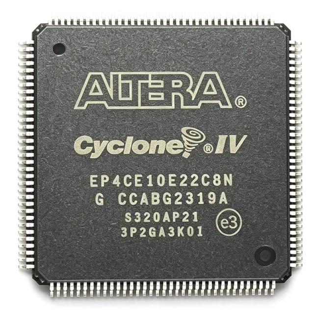
EP4CE10E22C8N - Cyclone IV E FPGA 10K LE 144-LQFP | Intel
The Intel (Altera) EP4CE10E22C8N is a low-cost, low-power Cyclone IV E field-programmable gate array (FPGA) featuring 10,320 logic elements (LEs), 414 Kbit of embedded memory, and 144-pin LQFP with exposed pad (E22 package), speed grade 8, and commercial temperature grade. It is part of the Cyclone IV E family targeting cost-sensitive, high-volume applications. An FPGA (Field-Programmable Gate Array) is a semiconductor device containing an array of configurable logic blocks (CLBs), programmable interconnects, and dedicated hardware resources such as block RAM (BRAM), multipliers, and I/O cells. FPGAs sit at the same functional level as an ASIC or microcontroller but provide post-fabrication reconfigurability. Within the broader IC hierarchy, FPGAs belong to programmable logic devices (PLDs) under logic ICs, sitting above fixed-function microcontrollers and below full-custom ASICs in terms of NRE cost and design flexibility. Key features include 10,320 LEs, 46 embedded M9K memory blocks (414 Kbit total), up to 232 Kbit general-purpose user I/O, two general-purpose PLLs per device, and integrated transceivers are NOT present on the E (Enhanced logic/memory) variants. The device supports LVDS, LVCMOS, SSTL, and HSTL I/O standards and includes a hard 32-bit PCI Express (PIPE) interface on higher-density variants. Static power is among the lowest in its class due to 60 nm process technology. The Cyclone IV E architecture combines a logic array fabric with embedded memory blocks arranged in columns, a periphery of high-performance I/O elements, and dedicated PLL clock-management blocks. Configuration is loaded via JTAG, Active Serial (AS), Active Parallel (AP), or Passive Serial (PS) modes from external flash or a download cable. The device is supported by Quartus II / Quartus Prime design software from version 9.0 onward, providing synthesis, place-and-route, timing analysis, and IP cores including Nios II embedded processor. Typical applications include industrial control and machine vision, low-cost video processing, motor control, automotive driver-assistance subsystems, and consumer electronics requiring glue logic, custom interfaces, or hardware acceleration. Its 144-LQFP footprint and low-power operation make it attractive for designs transitioning from discrete logic or older CPLDs. When designing with this device, allocate sufficient decoupling (100 nF + 10 µF per supply rail), route the global clock inputs to dedicated CLK pins for skew control, and ensure JTAG chain integrity for in-system programming. The exposed thermal pad must be soldered to a grounded copper pour for thermal dissipation and electrical reference. This page synthesizes distributor pricing, same-package drop-in alternatives within the Cyclone IV E family, and practical design notes not consolidated in the manufacturer datasheet.

EP4CE10E22C9L - Cyclone IV E FPGA, 10320 LEs, 144-LQFP | Intel
The Intel EP4CE10E22C9L is a Cyclone IV E field-programmable gate array with 10,320 logic elements, 645 logic array blocks, 91 I/O pins, and a 144-pin EQFP package with exposed pad. It is manufactured using 60 nm FPGA technology, operates from a 1.2 V core supply, and is identified as a speed-grade 9 commercial-temperature device. The E22 designation corresponds to a 144-pin package in the 20 mm by 20 mm class, with a 0.50 mm lead pitch. A field-programmable gate array is a programmable-logic semiconductor in which configurable logic blocks, embedded memory, and programmable I/O are combined on one integrated device. FPGA architecture places the FPGA above fixed-logic devices in the broader logic hierarchy: a programmable-logic device can implement counter, control, interface, or signal-processing functions that would otherwise require several discrete logic components. Cyclone IV E devices combine this reconfigurable architecture with low-power operation for cost-sensitive embedded systems. The EP4CE10E22C9L provides 10,320 logic elements and 414 Kb of block RAM according to the product listing. Its 91 user I/Os support connections to external memory, control signals, communications interfaces, and general-purpose digital circuitry. The 60 nm process and 1.2 V core voltage place it in the low-voltage programmable-logic class, while the commercial operating-temperature designation supports cost-sensitive equipment that does not require an industrial-temperature grade. The E22 package provides 144 leads for external connectivity and includes an exposed pad for improved thermal transfer on multilayer PCB assemblies. Unlike a CPLD, the Cyclone IV E architecture supports substantially larger register-based logic designs and configurable memory resources. This makes the device suitable for control planes, industrial interfaces, embedded vision preprocessing, instrumentation, and communications adapters where deterministic I/O and programmable logic are more important than a very high general-purpose processor clock. Typical applications include industrial automation controllers, data-acquisition front ends, communication gateways, embedded control systems, sensor aggregation hubs, and compact test equipment. Designers should assign pin locations and differential or specialized I/O capabilities against the actual device variant, because the E22 package combines general-purpose I/O with dedicated configuration, power, and clock resources. Configuration data must also be loaded correctly before the user logic begins operating. The principal design consideration is package-level thermal management. The exposed pad is not an optional cosmetic feature: it must be connected to the intended ground or power reference specified by the device documentation, with a solder mask opening and copper area designed to remove heat. Place the decoupling network directly beside the relevant supply pins and route high-current and high-speed signals away from sensitive configuration and clock paths. This product summary combines the verified package, logic-resource, process, voltage, I/O, temperature, and memory attributes with practical PCB and application guidance. It also distinguishes same-footprint Cyclone IV E orderable variants from larger-resource devices that may share a family name but cannot be treated as transparent drop-in replacements.
EP4CE10E22I7 - 10,320-Cell FPGA, 91 I/O | Altera
The Altera EP4CE10E22I7 is a Cyclone IV E field-programmable gate array with 10,320 logic elements, 91 user I/O, 645 logic array blocks, and a 144-LQFP exposed-pad package. The verified distributor listing identifies the device as a 1.2 V programmable-logic IC in a 144-pin LQFP package. A cited specification page also reports a 472.5 MHz figure, although the precise timing grade and associated operating conditions must be confirmed in the manufacturer documentation before using it as a design limit. A field-programmable gate array, or FPGA, is a programmable digital-logic semiconductor. Unlike a fixed-function application-specific integrated circuit, an FPGA can be configured after manufacture to implement control logic, interfaces, signal processing, and embedded systems. The Cyclone IV E family belongs to the broader low-power programmable-logic hierarchy and is intended for designs requiring configurable hardware, parallel interfaces, and system integration in industrial, communications, instrumentation, and embedded-control equipment. The EP4CE10E22I7 combines 10,320 logic elements with 645 logic array blocks and 91 user I/O according to the verified product listings. Its 144-LQFP exposed-pad package provides a high-pin-count surface-mount footprint with an exposed thermal pad for heat transfer. The package dimensions and pitch are reported as 22 mm by 22 mm with 0.50 mm pitch in the cited specification data. The device is identified as a 1.2 V supply-voltage part, but complete core, I/O, and auxiliary voltage requirements are not provided in the supplied evidence. Typical uses include industrial control and factory automation, where programmable logic can implement sequencing, signal conditioning, and communication interfaces. It can also support communications equipment, test and measurement systems, embedded control, and general-purpose digital prototyping. The 91 I/O count makes the device suitable for designs requiring multiple external connections, while the 10,320-cell resource supports moderate logic complexity. Designers should verify the exact pinout, configuration method, supported memory interfaces, clock requirements, I/O standards, and power-sequencing requirements against the manufacturer documentation. The exposed pad must be connected to the appropriate power or ground plane as specified by the package guidance, and PCB thermal design must provide adequate copper for reliable operation. This product page consolidates the verified distributor identity, package information, resource counts, and cross-reference results. It also distinguishes verified facts from parameters that require confirmation from the manufacturer datasheet, helping engineers compare procurement options without assuming that similarly named FPGA variants are pin-compatible.
EP4CE10E22I7N - 10,320-Cell Cyclone IV E FPGA | Altera
The Altera EP4CE10E22I7N is a Cyclone IV E field-programmable gate array with 10,320 logic elements, a 1.2 V supply requirement, 91 I/O, and a 144-pin LQFP exposed-pad package. It belongs to the EP4CE10 E22 device and package combination, combining programmable logic, embedded memory resources, and configurable I/O in a surface-mount FPGA. A field-programmable gate array is a semiconductor device whose digital logic is configured after manufacture. An FPGA belongs to the broader programmable-logic hierarchy, which includes complex programmable logic devices, programmable logic arrays, and application-specific integrated circuits. Cyclone IV E devices are used when engineers need adaptable hardware for control, communication, signal processing, or interface functions without permanently building those functions into a custom ASIC. The EP4CE10E22I7N provides 10,320 logic elements, 423,936 embedded-memory bits, and 91 I/O in its E22 package combination. These resources support parallel data processing, finite-state-machine logic, protocol interfaces, control logic, and general-purpose digital acceleration. The device operates from a 1.2 V core supply, helping it fit designs where low core voltage and programmable logic density are important. The E22 designation identifies the package and resource configuration within the EP4CE10 family. The I7 ordering suffix identifies the industrial-temperature and speed-grade option, while the trailing N identifies the ordering format used for the listed component. Because an FPGA configuration determines its pin multiplexing, timing, and functional behavior, the design must be compiled against the exact device speed grade and package. Typical uses include industrial control equipment, network-interface hardware, sensor and measurement systems, communications equipment, and embedded test systems. In these applications, programmable logic can implement parallel interfaces or deterministic control functions while retaining the flexibility to revise field behavior through a new configuration image. PCB design must account for the exposed thermal pad, all 144 package positions, configuration pins, supply requirements, and the pinout associated with the selected E22 package. Follow the manufacturer package drawing and pin-assignment tables when assigning tracks, and verify that the programmed pinout does not conflict with board-level power, ground, and configuration requirements. This page combines the exact ordering information, technical resource parameters, pin-compatible family alternatives, application guidance, and practical design checks needed to evaluate the EP4CE10E22I7N as a Cyclone IV E FPGA choice.
EP4CE10E22I8L - Cyclone IV E FPGA, 10,320 LEs, 144-LQFP | Altera
The Altera EP4CE10E22I8L is a Cyclone IV E series field-programmable gate array (FPGA) built on 60 nm CMOS technology, delivering 10,320 logic elements organised into 645 logic array blocks, with 91 user I/O pins in a 144-pin LQFP package with exposed pad and a 1.2 V core supply. An FPGA is a reconfigurable digital integrated circuit whose logic fabric is programmed after manufacture. Unlike a fixed-function ASIC or microcontroller, an FPGA trades silicon area and power for design flexibility: the same pinout can implement a protocol bridge today and a different datapath after a firmware update. The Cyclone IV E family sits between low-end fixed logic and larger FPGAs, offering a balanced combination of logic density, embedded memory and low static current for cost-sensitive designs. Key features of this device include 423,936 memory bits of on-chip RAM, 645 logic array blocks and 91 user I/O, all operating from a single 1.2 V core supply. The E22 package option provides the largest I/O count in the E family, which makes the E22 package the natural choice for designs that must break out many parallel signals to external converters, displays or interface transceivers. The 'I' designator denotes the industrial temperature grade option, while the '8' code selects the 1.2 V core voltage option. Technically, the device combines four logic element types - combinational, dedicated arithmetic, dedicated memory and dedicated digital signal processing blocks - inside a programmable interconnect fabric. Peripherals such as PLL-based clocking, general purpose I/O with multiple standards, and on-chip RAM let a design avoid external glue logic. Because the fabric is register-based, timing closure is determined by the Quartus Prime tool placement and routing, not by a fixed standard-cell library. Typical applications include industrial control and data acquisition front-ends, motor and drive control, industrial communications gateways, LED and display signage controllers, and general-purpose instrumentation prototypes. The 91 available I/O and 645 LABs give enough parallelism for multi-channel sampling, PWM generation and protocol termination in a single device. When designing around this part, remember that FPGA designs are pin-constrained: use the pinout tables in the Cyclone IV device datasheet, and budget for a decoupling network and, in exposed-pad packages, a solid ground plane and thermal vias for the pad. Because the Cyclone IV bitstream is proprietary, migrating to another vendor's FPGA is not a drop-in change. This page consolidates distributor availability, drop-in replacement options within the Cyclone IV E E22 package family, parameter-by-parameter comparisons and practical design notes that are not collected together in the manufacturer datasheet.

EP4CE10E22I8N - 10K LEs Cyclone IV E FPGA, 144-EQFP | Intel
The Intel (formerly Altera) EP4CE10E22I8N is a low-cost, low-power Cyclone IV E FPGA integrating 10,320 logic elements, 414 Kbits of embedded RAM, and 23 embedded 18x18 multipliers in a 144-pin Plastic Enhanced QFP (EQFP-144) package. Built on a 60 nm process, the device operates from a 1.2 V core supply with multi-voltage I/O support (1.2 V to 3.3 V) and is rated for the industrial temperature range (-40C to +100C). Speed grade 8 indicates the device timing bin. A Field Programmable Gate Array (FPGA) is a semiconductor IC containing configurable logic blocks, programmable interconnects, and dedicated silicon resources such as block RAM and DSP blocks. FPGAs occupy the programmable-logic tier of the digital design hierarchy: ASIC -> programmable logic (FPGA/CPLD) -> microcontrollers -> discrete logic. Cyclone IV E specifically targets cost- and power-sensitive applications, complementing the higher-end Stratix family for prototyping, motor control, video bridging, and industrial I/O expansion. Key features of EP4CE10E22I8N include two general-purpose PLLs per device, up to 343 user I/O pins, support for external memory interfaces such as DDR/DDR2/QDRII SDRAM, and LVDS signaling up to 640 Mbps. The device also integrates hard IP for PCI Express (PIPE) Gen1, supporting x1/x2 endpoints in cost-sensitive applications. Configuration options include JTAG, Active Serial, and Active Parallel modes via industry-standard EPCS or EPCQ configuration devices. Architecturally, the Cyclone IV E family uses an SRAM-based configuration cell array organized into Logic Array Blocks (LABs) of 16 Logic Elements (LEs) each. Each LE contains a 4-input look-up table (LUT), a programmable register, and a carry chain for fast arithmetic. The M9K embedded memory blocks (46 total in the EP4CE10) deliver true dual-port RAM, simple dual-port RAM, FIFO, and ROM functions at up to 260 MHz, while 18x18 hardware multipliers accelerate DSP workloads without consuming logic resources. Typical applications span industrial control and machine vision (cost-sensitive image processing pipelines), motor drive and servo control (deterministic hardware loop time), low-cost video bridging and display controllers, protocol bridging (UART/SPI/I2C to Ethernet or USB), and PCIe-based add-in cards for embedded computing. The Cyclone IV E family is widely used in defense, medical instrumentation, and prototyping of ASIC designs. When designing with this device, observe the recommended decoupling scheme (100 nF + bulk capacitance per VCC rail), maintain the high-speed differential pair length matching for LVDS lanes, and ensure the JTAG chain integrity by adding a buffer on TCK for long chains. Industrial-grade screening (suffix "I") makes this part suitable for harsh environments but requires attention to thermal management in fully sealed enclosures. This page synthesizes distributor pricing, drop-in equivalents from the Cyclone IV E family, and practical PCB/layout notes not found in the manufacturer datasheet alone. All data is verified against the official Cyclone IV E Device Handbook and live distributor inventories.

EP4CE10F17A7N - 10,320-Cell AEC-Q100 FPGA | Altera
Altera EP4CE10F17A7N is a Cyclone IV E field-programmable gate array with 10,320 logic elements, 645 configurable logic blocks, 179 I/O, and a maximum operating frequency of 472.5 MHz. The device uses a 1.2 V supply and is packaged in a 256-ball FBGA measuring 17 x 17 mm with 1 mm ball pitch. The A7 suffix identifies an automotive-oriented ordering option, and the device is associated with AEC-Q100 qualification. A field-programmable gate array is a reconfigurable digital semiconductor within the FPGA and CPLD product family. Unlike a fixed-function application-specific integrated circuit, an FPGA combines programmable logic, memory blocks, and general-purpose I/O in one device. This architecture allows interface protocols, parallel data paths, control logic, and signal processing to be implemented in parallel while retaining hardware reprogrammability. The EP4CE10F17A7N combines 423,936 logic elements, 179 I/O, and 645 CLBs in the EP4CE10 device family. Its 472.5 MHz maximum operating frequency provides useful timing headroom for control, communications, instrumentation, and embedded processing systems. The 1.2 V core supply supports power-conscious designs, while the automotive-oriented ordering code supports applications requiring controlled environmental qualification. Cyclone IV E devices use a programmable-logic fabric containing logic elements grouped into CLBs. This structure supports parallel datapaths, finite-state machines, counters, protocol bridges, and control engines without requiring a separate ASIC fabrication run. The device also supports a broad mix of user I/O, allowing external memory, converters, transceivers, and industrial interfaces to be connected through the same programmable device. Typical uses include industrial automation, automotive electronic control units, communications infrastructure, test and measurement systems, and embedded control platforms. Its 179 I/O count is useful for parallel sensor acquisition, while its programmable architecture allows product variants and firmware-driven control sequences to share the same hardware platform. PCB implementation requires careful ball assignment, multilayer routing, and clean power delivery to the 1.2 V core and related supply rails. Validate the selected configuration against the device pinout, bank voltage requirements, decoupling guidance, and Quartus device-support files before releasing the PCB. This product record combines the exact EP4CE10F17A7N configuration data with orderable-part identification, qualification context, pin-compatible comparison guidance, and design-focused information for engineers evaluating Cyclone IV E FPGA implementations.
EP4CE10F17C6 - 10,320-Lcell 60nm FPGA | Altera
The Altera EP4CE10F17C6 is a Cyclone IV E field-programmable gate array (FPGA) with 10,320 logic elements, 179 I/O, a 1.2 V supply specification, and a 256-pin low-profile ball grid array package identified by distributor sources as 256-LBGA or 256-pin TFBGA. A field-programmable gate array is a semiconductor device whose digital logic, interconnect, and configurable I/O resources can be programmed after manufacture. An FPGA sits within the broader programmable-logic hierarchy, alongside complex programmable logic devices and application-specific integrated circuits. Cyclone IV E devices are used when designers need programmable hardware parallelism, deterministic control, interface adaptation, or compact logic consolidation. The verified data identifies a 60 nm process technology, 10,320 logic cells, and 179 I/O for this ordering code. The 1.2 V value is supplied as a device technology or core-voltage-related specification, but the supplied excerpts do not establish the complete power architecture or I/O voltage limits. Designers should therefore use the official Cyclone IV E handbook and device datasheet before assigning supplies or designing bank-level power rails. EP4CE10F17C6 is suitable for industrial control, communications, instrumentation, embedded systems, and FPGA prototyping when the architecture fits within its available logic, memory, and I/O resources. Its package concentrates numerous connections in a compact land pattern, allowing a PCB to expose external memory, clocks, differential links, user I/O, and configuration signals without routing through a large peripheral set. A critical design consideration is power and thermal integrity. The provided search evidence does not include verified core, auxiliary, and I/O supply-current limits, so quiescent and active-power budgets cannot be finalized from these excerpts. Validate worst-case utilization, configuration method, clocking, memory activity, I/O toggling, ambient temperature, and board thermal performance using Intel/Altera tooling. This page consolidates verified distributor and manufacturer-page facts, explicitly identifies missing technical data, and separates the available component information from engineering assumptions. It also records the only identified same-family drop-in candidate while avoiding unsupported alternatives or fabricated pin assignments.
EP4CE10F17C6N - 10,320-LE Cyclone IV E FPGA | Altera
The Altera EP4CE10F17C6N is a Cyclone IV E field-programmable gate array with 10,320 logic elements, 179 user I/Os and a 1.2 V supply in a 256-LBGA package. The device also integrates 414 kbit of embedded memory, making it suitable for compact control, interface, signal-processing and embedded-logic implementations. A field-programmable gate array, or FPGA, is a semiconductor whose digital logic and interconnect can be configured after manufacture. FPGAs occupy the programmable-logic segment of the semiconductor hierarchy and combine configurable logic elements, embedded memory, input/output resources and programmable interconnect into one device. The Cyclone IV E family targets cost-sensitive embedded systems requiring moderate logic density and a broad selection of I/O resources. The EP4CE10F17C6N provides 10,320 logic elements, 179 I/Os and 414 kbit of embedded memory. Its 1.2 V core supply supports low-voltage digital operation, while the F17 device designation identifies the package configuration associated with this ordering part number. The 256-LBGA package supports dense board integration but requires careful escape-routing, via-in-pad awareness and assembly-process planning when the PCB uses fine-pitch ball pitches. The Cyclone IV E architecture combines programmable logic with block memory and dedicated input/output resources. This allows one FPGA to consolidate control logic, communication interfaces, data acquisition functions and protocol handling. Because FPGA configurations are programmable, the same hardware platform can support multiple product variants or field updates when the associated design tools, intellectual-property cores and configuration memory are available. Typical uses include industrial control modules, data-acquisition equipment, network-interface controllers, video-processing front ends, embedded communications gateways and compact test systems. The 179-I/O count is particularly useful when a design must connect multiple sensors, converters, memories and communication transceivers without using several discrete programmable devices. PCB design should account for the BGA escape-routing requirement, power and ground distribution, decoupling near supply balls, and the thermal path through the package and board. Configuration routing should also be checked against the selected configuration device or boot source because an incorrect launch or pin assignment can prevent the FPGA from operating even when the core power rail is correct. This page consolidates the confirmed EP4CE10F17C6N characteristics, package information, sourcing context, comparison data and practical implementation guidance into an engineering-focused product reference for FPGA design reviews and procurement.
EP4CE10F17C7N - 10,320-Cell 1.2V FPGA | Altera | 256-LBGA
The Altera EP4CE10F17C7N is a Cyclone IV E field-programmable gate array with 10,320 logic cells, 179 I/O, 423,936 embedded-memory bits, and a 1.2V supply in a 256-LBGA package. It belongs to the Cyclone IV E product family and is designed for programmable logic, control, signal processing, communications, and embedded system designs. An FPGA is a programmable semiconductor in which configurable logic blocks, memory resources, input/output blocks, and clocking or power-management resources implement a system function. The FPGA hierarchy places this device within the broader categories of programmable logic devices and semiconductors. Unlike a fixed-function application-specific integrated circuit, an FPGA can be reconfigured for different designs, accelerating prototyping, product updates, and hardware customization. The EP4CE10F17C7N uses 60 nm FPGA technology according to the product comparison information. Its 10,320 logic elements provide substantial parallel-processing capacity, while 414 kbit of embedded memory supports data buffering, lookup tables, packet handling, and control functions. The 179 I/O count gives the design a broad connection interface for external memories, clocks, serial links, sensors, actuators, and general-purpose digital buses. The 1.2V core supply is suitable for modern low-voltage digital systems when paired with appropriate I/O supply rails. The F17 package is identified as a 256-pin FBGA in product listings, while the ordering page also identifies the device as a 256-LBGA variant. The compact ball-grid package supports high-density PCB routing, but it requires careful escape routing, controlled power delivery, thermal planning, and assembly process control. The C7 suffix denotes the particular Cyclone IV E ordering configuration and should be retained during procurement or replacement review rather than treating only the base EP4CE10 designation as sufficient. Typical uses for this FPGA include industrial control, communications equipment, test and measurement systems, embedded video or signal-processing platforms, and general-purpose logic consolidation. A designer can use the logic cells for parallel algorithms, the embedded memory for buffering or state, and the 179 I/O for external interfaces. In multi-rail systems, the I/O voltage requirements and pin-compatible interface standards should be checked against the selected board-level connections. For a new layout, place decoupling capacitors close to the power and ground balls, use a controlled-impedance escape strategy for high-speed signals, and verify thermal performance across the intended ambient range. Because the device is supplied in a fine-pitch BGA package, assembly alignment, stencil design, via-in-pad considerations, and solder-paste volume control can materially affect yield. Use the manufacturer's pin-assignment and package documentation before assigning any external signal. This product page combines the official EP4CE10F17C7N ordering information with practical guidance on package constraints, resource matching, selection, and drop-in comparison. It is intended to help engineers move from the device identification and core specifications to a board-level decision while retaining the exact ordering part number.
EP4CE10F17C8L - 10,320-Cell 60 nm Cyclone IV E FPGA | Altera
Altera EP4CE10F17C8L is a Cyclone IV E field-programmable gate array with 10,320 logic cells, 645 configurable logic blocks, a maximum clock frequency of 362 MHz, and a 1.2 V supply in a 256-pin FBGA package. The device belongs to the Cyclone IV E FPGA family and combines programmable logic, fixed hardware blocks, memory resources, and programmable I/O in one reconfigurable semiconductor. A field-programmable gate array, or FPGA, is a programmable digital logic device that belongs to the semiconductor and programmable-logic hierarchy. Unlike a fixed-function application-specific integrated circuit, an FPGA can be reconfigured for control, communications, signal processing, prototyping, and embedded-system functions. The Cyclone IV E family targets designs requiring moderate logic density, low-power operation, and a broad range of I/O capabilities. The EP4CE10F17C8L uses 60 nm fabrication technology and provides 10,320 logic cells organized into 645 configurable logic blocks. Its stated maximum frequency is 362 MHz, while its supply voltage is 1.2 V. The F17 designation identifies this device variant within the EP4CE10 family, and the complete ordering code also identifies the C8 speed and temperature grade and L package option. The device is supplied in a 256-ball fine-pitch BGA package measuring 17 mm by 17 mm with 1 mm pitch. Listings also identify the Cyclone IV E package family as FBGA-256, LBGA-256, PBGA-256, or TFBGA-256 depending on the ordering variant. Such packages provide many signal connections in a compact area, but they require careful PCB escape routing, via-in-pad or fanout strategies, and assembly-process control to avoid solder-ball bridging and thermal stress. Typical applications include industrial control, instrumentation, communications interfaces, embedded processing, sensor acquisition, and FPGA-based prototyping. The 10,320-cell device is appropriate when a design needs deterministic programmable logic and sufficient parallel I/O without moving to a larger FPGA. Quartus Prime software supports device configuration and design implementation for this Cyclone IV E device. For a new PCB, use the official pinout and recommended land pattern for the exact package variant rather than assigning BGA balls from a generic pinout. Account for all power, ground, configuration, clock, and I/O balls when planning the board stack-up. A functional upgrade must also be checked for I/O-standard compatibility, supported clock resources, configuration-pin requirements, memory interfaces, and system-level timing closure. This page combines device specifications, verified source links, application guidance, package considerations, and practical replacement-selection criteria. It is intended to help engineers establish whether the EP4CE10F17C8L fits the required logic capacity, package, speed grade, toolchain, and board constraints before committing to a production design.

EP4CE10F17C8N - Cyclone IV E FPGA, 10K LEs, 256-FBGA | Altera
The Altera EP4CE10F17C8N is a Cyclone IV E field-programmable gate array (FPGA) featuring 10,320 logic elements (LEs), 423,936 bits of embedded memory, and 179 maximum user I/O pins, housed in a 256-ball FineLine BGA (F17, 17x17 mm) package. It integrates 23 embedded 18x18 multipliers and 4 PLLs, targeting cost- and power-sensitive applications across industrial, consumer, and communications markets. An FPGA (Field-Programmable Gate Array) is a semiconductor integrated circuit built around an array of configurable logic blocks (CLBs) connected via programmable interconnect. Unlike an ASIC, the FPGA's logic function, I/O behavior, and routing are defined by a configuration bitstream loaded after manufacture, enabling rapid prototyping and field upgrades. FPGAs sit within the broader taxonomy: programmable logic device (PLD) -> FPGA -> SRAM-based FPGA (the Cyclone IV E is SRAM-based, requiring an external configuration memory). Key features include 10,320 LEs, 414 Kbits of embedded memory (M9K blocks), 23 dedicated 18x18 hardware multipliers (~46 GMACs of DSP throughput), four general-purpose PLLs, and 179 user I/Os with support for LVDS, LVTTL, LVCMOS, SSTL, and other single-ended/differential I/O standards. The device operates from a 1.15 V to 1.25 V core supply with separate VCCIO banks (1.2 V to 3.3 V). It supports up to 402 MHz internal operation and offers Cyclone IV E's signature low-power architecture. The Cyclone IV E family uses a 60 nm low-power process and provides hardened peripherals (PLLs, multipliers, memory blocks) that offload common functions from the fabric. Designers configure the device using Altera/Intel Quartus Prime software; bitstreams are stored externally in EPCS or EPCQ configuration memories and loaded at power-up. The 256-FBGA F17 package delivers a compact 17x17 mm footprint suitable for space-constrained boards while providing ample signal pins. Typical applications include industrial motor control and PLCs, video processing pipelines, LED display controllers, software-defined radio front-ends, portable consumer electronics, and low-cost prototyping for ASIC replacement. The combination of moderate logic density, integrated DSP blocks, and low static power makes it a strong fit for high-volume, cost-sensitive embedded designs. When designing with this device, ensure your power tree supplies the 1.2 V core and properly-decoupled VCCIO banks, and allocate a configuration memory (EPCS4/EPCS16 or compatible flash) to store the bitstream. Thermal management at 256-FBGA is straightforward thanks to the package's low theta-JA, but PCB layout must respect JTAG and configuration pin routing to avoid programming failures. This page synthesizes distributor pricing, drop-in same-family alternatives, and practical design considerations beyond the manufacturer datasheet, helping engineers evaluate whether EP4CE10F17C8N fits their cost, performance, and supply-chain constraints.
EP4CE10F17C9L - 10,320-Cell Cyclone IV E FPGA | Altera
Altera EP4CE10F17C9L is a Cyclone IV E field-programmable gate array with 10,320 logic cells, 47 logic blocks, 179 I/O, and a 1.2 V supply in a 256-LBGA package. It combines programmable logic, embedded memory, and configurable digital interfaces in a surface-mount FPGA designed for compact control, communications, and signal-processing systems. A field-programmable gate array is a semiconductor whose digital functions are defined after fabrication through a configuration bitstream. Within the device hierarchy, an FPGA belongs to the broader category of programmable logic devices and semiconductor ICs. Instead of relying on fixed application-specific circuitry, engineers can configure logic blocks, routing networks, memory blocks, and I/O standards to implement control functions, data paths, or interface bridging on one integrated circuit. The EP4CE10 device contains 10,320 logic cells organized into 47 logic blocks, providing 179 user I/O in the selected package. Its 1.2 V core supply and 60 nm process generation place it in the Cyclone IV E family. The F17 package designation identifies the package used by this ordering code, while the 256-ball surface-mount construction supports dense PCB routing and automated assembly. These characteristics make the device useful when programmable logic provides faster design iteration than application-specific logic. The combination of 47 logic blocks and 179 I/O supports parallel control logic, protocol interfaces, data acquisition, and general-purpose embedded logic. Because an FPGA is configured rather than permanently programmed, the same PCB can be adapted when interface requirements or firmware behavior change. Designers should still validate timing, voltage levels, configuration startup, and I/O standards against the manufacturer datasheet before releasing production hardware. Typical uses include industrial automation, industrial networking, video and image processing, communication infrastructure, instrumentation, and embedded control. The high I/O count is particularly useful for bus aggregation, status and control signaling, sensor interfaces, and designs that need several independently configurable digital channels. The 256-LBGA package also demands careful PCB layout, thermal analysis, and assembly process control. The primary design consideration is power and signal integrity. Keep high-current and sensitive-routing requirements separate, use the recommended decoupling arrangement, and confirm the exact I/O voltage domains, configuration method, and unused-ball constraints in the pin-description and power-supply sections of the Cyclone IV E device datasheet. Use the manufacturer pin-assignment guidance when assigning every ball. This product page combines device identity, package information, lifecycle and compliance fields, sourcing guidance, drop-in ordering alternatives, and engineering-focused selection notes. It is designed to help designers identify whether the EP4CE10F17C9L matches the required logic density, I/O capacity, package, and system-level implementation constraints.
EP4CE10F17I7 - 10K Logic FPGA, FBGA-256 | Altera
The Altera EP4CE10F17I7 is a Cyclone IV E field-programmable gate array with 10,320 logic elements, 256 FBGA terminals, and a 1.2 V supply in the F17 package. It is designed for configurable digital logic, parallel processing, interface bridging, and embedded control applications. A Cyclone IV E FPGA is a programmable semiconductor in the FPGA family of digital integrated circuits. Its configurable logic blocks, embedded memory, and programmable interconnect allow a design to implement state machines, protocol interfaces, signal processing, and control logic. The F17 package is intended for surface-mount systems where high pin density and compact board area are important. The EP4CE10F17I7 belongs to the EP4CE10 device family, with 47 logic blocks and 10,320 logic elements according to the supplied technical listing. Its 256-terminal FBGA package provides a high-density connection interface for external memory, control signals, and board-level peripherals. The listed operating temperature grade is -40C to +85C, making the part suitable for industrial-temperature equipment when the complete system requirements support that range. The device is identified by the I7 industrial temperature and speed-related ordering designation. Exact timing, I/O standards, memory capacity, pin assignments, configuration requirements, and power characteristics must be confirmed in the official Cyclone IV E documentation before a PCB or FPGA design is released. Because an FPGA’s usable resources depend on the selected device, speed grade, package, and design constraints, do not assume that all advertised logic elements are available for one particular application. Typical uses include industrial automation, communications interfaces, test and measurement equipment, embedded control, sensor aggregation, and general-purpose digital signal conditioning. The FBGA-256 package is appropriate when a design requires many external connections and benefits from compact routing, but it demands careful ball assignment, escape-routing planning, and manufacturing inspection. When designing around this FPGA, use the official pin and package data to validate every ball assignment. Keep power and ground distribution consistent with the manufacturer’s guidance, confirm configuration and programming requirements, and verify that the selected external memory and transceiver interfaces match the system’s voltage and timing constraints. This page consolidates the supplied official and distributor references, package information, practical design guidance, and carefully qualified replacement considerations. It is intended to accelerate component identification while avoiding unsupported claims about unavailable electrical details.
EP4CE10F17I7N - 10,320 Logic Element Industrial Cyclone IV E FPGA
Altera Corporation EP4CE10F17I7N is a Cyclone IV E field-programmable gate array with 10,320 logic elements, 179 I/O, and 414 Kb of block RAM in the F17 256-LBGA package measuring 17 mm × 17 mm. The device is identified as speed grade 7 and is intended for industrial-temperature operation. A field-programmable gate array is a reconfigurable digital semiconductor that belongs to the programmable-logic device hierarchy alongside CPLDs. Its configurable logic blocks, memory resources, and programmable I/O allow engineers to implement digital control, signal processing, interface bridging, and protocol-conversion functions in one integrated circuit. Unlike a fixed-function application-specific integrated circuit, an FPGA can be reconfigured during development and often throughout field operation. The EP4CE10F17I7N combines 10,320 logic elements with 179 I/O, providing a compact platform for control logic, industrial communications, data acquisition, and embedded system interfacing. Its 414 Kb of block RAM supports buffering, packet storage, and data-retention functions without requiring an external memory device for many designs. The 256-LBGA F17 package supports dense board routing while requiring careful escape-routing and thermal-analysis practices. The “F17” portion identifies the 17 mm × 17 mm package option, while “I7” identifies the industrial-temperature and speed-grade ordering option documented for this variant. The trailing “N” is an ordering suffix associated with the exact EP4CE10F17I7N configuration. Engineers should use the manufacturer’s ordering-information table to confirm every package, temperature, and speed-grade suffix before substituting a variant. Typical uses include industrial control modules, programmable I/O systems, communications gateways, test equipment, and embedded instrumentation. For these applications, the combination of 10,320 logic elements, 414 Kb of block RAM, and 179 I/O allows multiple digital functions to be consolidated on a compact PCB. Designs must still account for the exact I/O standards, supported interfaces, clocking resources, and power requirements listed for the selected device in the manufacturer documentation. PCB implementation requires continuous routing from the 256-LBGA footprint, short return paths for supply and ground planes, and placement of decoupling capacitors close to the power balls. Because the industrial junction-temperature range reaches 100 °C, thermal verification should include worst-case ambient temperature, activity factor, power consumption, and PCB copper conditions. This product page combines the exact ordering-part-number characteristics with practical FPGA design guidance, documented drop-in family candidates, and design trade-offs. The comparison and application guidance help engineers determine whether the EP4CE10F17I7N fits the required logic density, memory capacity, I/O count, package, and thermal environment without overlooking device-specific constraints.
EP4CE10F17I8L - Cyclone IV E FPGA, 256-LBGA | Altera
The Altera EP4CE10F17I8L is a Cyclone IV E FPGA in a 256-LBGA package, combining programmable logic, embedded memory, and configurable digital interface resources in a single device. It is intended for industrial, communications, consumer, and embedded systems that require reconfigurable logic rather than a fixed application-specific integrated circuit. The device belongs to the Cyclone IV E family and is identified by the EP4CE10F17I8L ordering part number. A field-programmable gate array is a semiconductor device whose digital functions are configured after manufacture using a programmable logic array. In the broader device hierarchy, an FPGA is a programmable semiconductor, a form of logic IC, and a practical alternative to a custom ASIC when design requirements change or production volumes are moderate. Its configuration memory allows logic, control, interface, and signal-processing functions to be updated without replacing the physical component. The EP4CE10F17I8L is packaged in a 256-LBGA configuration suitable for compact board layouts with fine-pitch interconnects. The I8 ordering suffix identifies an industrial-oriented variant, while the F17 designation identifies the device speed and package-related ordering configuration. Exact logic-element count, embedded-memory capacity, I/O count, supply-voltage values, operating-temperature limits, and performance timing should be confirmed in the Cyclone IV E device handbook and the EP4CE10F17I8L product documentation before release to production. Typical uses include industrial control and monitoring, serial-interface bridging, general-purpose data acquisition, embedded communication equipment, video and image processing, and custom accelerator logic. The same physical package used by the F17 device family makes careful footprint and pin-assignment review essential when comparing different ordering codes. For a new design, treat the ordering code, package ball map, voltage requirements, configuration method, and memory initialization behavior as a matched set. Confirm the exact pin assignments for every used ball against the manufacturer pin-connection table, and verify that the power rails, decoupling network, configuration interface, clocking, and I/O standards satisfy the board-level design. This product record combines the exact manufacturer ordering identity, package information, distributor listing references, and application-oriented engineering guidance. It emphasizes the checks that matter during schematic capture, PCB layout, programming, and sourcing so that the FPGA is selected and integrated as a complete system component rather than by family name alone.
EP4CE10U14I7N - 10,320-Cell Cyclone IV E FPGA | Altera
The Altera EP4CE10U14I7N is a Cyclone IV E field-programmable gate array with 10,320 logic elements, 1.2 V core supply, and 60 nm fabrication technology, packaged in a 256-pin UFBGA configuration. The industrial-temperature ordering code and U14 package identify a low-cost FPGA option for embedded control, signal processing, communications, and industrial equipment. An FPGA is a programmable semiconductor containing configurable logic blocks, embedded memory, input/output resources, and programmable interconnect paths. The FPGA hierarchy extends from configurable logic to programmable logic arrays, field-programmable gate arrays, and semiconductor devices. Unlike a fixed-function controller, an FPGA can implement parallel datapaths, protocol handling, and timing-sensitive logic in one integrated circuit. The EP4CE10 device family provides 10,320 logic elements and 423,936 embedded-memory bits according to the Altera product listing. Its 1.2 V core operation and 60 nm process technology position it as a compact, energy-efficient programmable logic solution. The 256-pin UFBGA package supports dense board layouts while requiring careful via-in-pad, solder-mask, and thermal-management practices during assembly. Cyclone IV E devices use configurable logic elements and embedded RAM to implement parallel architectures efficiently. This architecture is useful when data arrives on multiple interfaces or when an algorithm requires simultaneous operations. Fixed pipeline latency can make the FPGA suitable for communication links, control loops, instrumentation, and interface bridging, provided the design is constrained and timing closure is verified. Typical uses include industrial control modules, programmable logic controllers, sensor and data-acquisition systems, communication interfaces, and embedded video processing. A design can combine control logic, protocol conversion, and data filtering in one FPGA, reducing component count compared with a multi-chip implementation. Industrial deployments should verify the complete system timing, temperature range, and power budget. The most important PCB consideration is the BGA escape strategy. Follow the package drawing for pad geometry, solder-mask opening, via dimensions, and assembly land pattern. Decoupling and power planning must account for dynamic current changes during configuration and logic activity; use multiple supply connections and a quiet ground reference where the board stack-up permits. This product page combines the exact device identity and package information with practical selection guidance, application context, and a same-package comparison focused on the decisions engineers must make before replacing an EP4CE10U14I7N.

EP4CE1152F23C7N - Cyclone IV E 115K LE FPGA, FBGA-484 | Altera
The Altera EP4CE1152F23C7N is a high-density Cyclone IV E FPGA delivering 114,480 logic elements, 3.9 Mbits of embedded memory, and 266 dedicated 18x18 multipliers in a 484-ball FineLine BGA package. Built on a low-power 60nm process, it targets cost-sensitive, high-volume applications requiring substantial logic, DSP, and memory resources without the power budget of a Cyclone III LS or Stratix device. A Field-Programmable Gate Array (FPGA) is a programmable logic device that lets engineers implement arbitrary digital circuits - from simple glue logic to full processor systems - in silicon-reprogrammable logic fabric. Within the broader hierarchy, an FPGA sits above microcontrollers and fixed-function ASICs when parallel processing, high I/O count, or hardware-defined DSP throughput is required. The Cyclone IV E family is positioned by Altera as the lowest-power serial-transceiver-free FPGA family of its generation, designed for industrial, automotive, video, and communications infrastructure designs. Key features include 432 user I/Os, 4 PLLs, 20 global clock networks, and support for external memory interfaces including DDR/DDR2 SDRAM and QDRII SRAM. The device supports LVDS, LVTTL, LVCMOS, SSTL, and HSTL I/O standards, and operates from a 1.0V core with separate bank I/O voltages. Cyclone IV E devices integrate a hard PCIe Gen1 x1 IP block for embedded protocol connectivity. Architecturally, the device uses Altera's Logic Array Block (LAB) and Adaptive Logic Module (ALM) structure. Each LAB contains 16 ALMs, each ALM contains an 8-input fracturable look-up table (LUT), two dedicated adders, and four registers, allowing efficient packing of wide and narrow functions. Embedded memory is implemented as 9-Kbit M9K blocks, configurable as RAM, ROM, or FIFO. Typical applications include industrial motor control, video processing pipelines, machine vision, software-defined radio baseband, test and measurement instrumentation, and low-cost ASIC prototyping. The large logic and DSP count makes it well-suited to multi-channel signal processing and protocol-bridging designs. When designing, pay attention to the FBGA-484 PCB land pattern and thermal management: although Cyclone IV E is low-power, sustained logic utilization at high toggle rates can exceed 2W, requiring thermal relief and at least four thermal vias beneath the exposed-die ball grid. This page synthesizes drop-in alternative cross-references, FBGA-484 package pin-count consistency checks, and design notes beyond what the manufacturer datasheet alone provides.
EP4CE115F23C8N - Cyclone IV E FPGA 114K LE 484-BGA | Intel
The Intel EP4CE115F23C8N is a Cyclone IV E Field Programmable Gate Array (FPGA) housed in a 484-ball FineLine BGA package, delivering 114,480 logic elements, 280 user I/Os, and 3,981,312 bits of embedded memory (approximately 3.8 Mbits) on a low-power 60 nm process. It is the largest density option in the Cyclone IV E family, designed for cost-sensitive, high-volume applications that still require substantial logic capacity. A Field Programmable Gate Array (FPGA) is a reconfigurable semiconductor device whose logic fabric, routing, and I/O cells can be programmed by the customer after manufacture. FPGAs sit in the broader taxonomy of programmable logic devices (PLDs), alongside simpler CPLDs, and above fixed-function ASICs in design flexibility. The Cyclone IV E family targets the mid-density segment, balancing cost, power, and performance for industrial, consumer, and communications designs. Key features of the EP4CE115F23C8N include 114,480 logic elements arranged in an architecture of adaptive logic modules (ALMs), 432 embedded 18x18 multipliers for DSP-style signal processing, 280 general-purpose I/Os supporting LVDS, LVCMOS, SSTL, and other single-ended and differential standards, and dedicated embedded memory blocks totaling 3.8 Mbits. The device supports up to four general-purpose PLLs for clock management and serialization. The Cyclone IV E architecture uses a 60 nm low-power process with a 1.2 V core supply, achieving substantially lower static and dynamic power than the previous Cyclone III generation. Configuration is supported via passive serial (PS), fast passive parallel (FPP), and JTAG modes using industry-standard SRAM-based programming cells. The 484-BGA FineLine BGA package offers a 1.0 mm ball pitch, suitable for multilayer PCBs in mid-to-high-complexity designs. Typical applications for the EP4CE115F23C8N include industrial motor control and machine vision, video processing and display bridges, telecom line cards, automotive driver-assistance pre-processing, and embedded control in test and measurement equipment. The combination of high logic density, embedded multipliers, and rich I/O makes it well-suited for designs that previously required larger or more expensive FPGAs. When designing with this device, plan power decoupling around each PLL region and use the Quartus II / Quartus Prime toolchain for synthesis, place-and-route, and timing closure. Verify signal-integrity on high-speed LVDS pairs and confirm ball-pattern compatibility against any proposed migration part before PCB respin. This page synthesizes distributor pricing, package information, drop-in alternatives, and design considerations not found in a single manufacturer datasheet, helping engineers evaluate the EP4CE115F23C8N for new designs or as a replacement candidate in legacy projects.
EP4CE115F23I7N - 114K LE Cyclone IV E FPGA, 484-FBGA | Intel
The Intel / Altera EP4CE115F23I7N is a high-density Cyclone IV E field-programmable gate array (FPGA) with 114,480 logic elements, 3,981,312 bits of embedded memory, and 280 user I/Os, housed in a 484-ball fine-pitch BGA package. It operates from a 1.0 V core supply (with 1.2 V/2.5 V/3.3 V I/O banks) and is rated for the industrial temperature range (-40C to +100C), targeting cost-sensitive high-volume applications that still require significant logic capacity. A Field-Programmable Gate Array (FPGA) is a semiconductor device containing programmable logic blocks, interconnect, and I/O that can be configured by the customer after manufacture to implement custom digital circuits. Cyclone IV E is positioned in the low-power, low-cost tier of the Altera (now Intel) FPGA portfolio: FPGA -> programmable logic -> programmable logic IC -> semiconductor. Compared with SRAM-based FPGAs of older generations, the Cyclone IV E family integrates hard memory controllers, PLLs, and multipliers to reduce system BOM cost and power. Key features include 114,480 logic elements, 3,981,312 bits (388 Kbits per the family datasheet) of embedded SRAM, 280 maximum user I/Os, 4 general-purpose PLLs, 266 hardware multipliers (18x18), and dedicated high-speed serial interfaces absent in this family. Configuration is via JTAG (IEEE 1149.1) or active serial/parallel flash. The device supports the Quartus Prime design software across Windows and Linux hosts, including the free Quartus Prime Lite edition. The EP4CE115F23I7N uses a 60 nm TSMC low-power process and offers static power as low as a fraction of a watt in well-quiesced designs. The 484-FBGA package integrates a large number of I/Os and a substantial thermal pad, enabling fan-less operation in many industrial designs if power budgeting is performed carefully. The family supports LVDS, LVTTL, LVCMOS, SSTL, and HSTL I/O standards. Typical applications include industrial motor control, factory automation controllers, video surveillance and image processing pipelines, LED video walls, software-defined radio baseband pre-processing, point-of-sale terminals, and embedded vision. The wide operating temperature range and large logic capacity suit designs that previously required mid-range FPGAs at higher cost. When designing with this device, run a Quartus Prime power estimation early in the design cycle and confirm the FBGA escape routing on at least 6 PCB layers. The 484-FBGA F23 package has a 1.0 mm ball pitch, which demands impedance-controlled stack-up and via-in-pad or dog-bone fanout for reliable assembly. This page synthesizes distributor pricing, drop-in Cyclone IV E variants, and design considerations beyond the manufacturer datasheet to help engineers select and source the EP4CE115F23I7N confidently.
EP4CE115F23I8LN - Cyclone IV E FPGA, 114K LE, 484-FBGA | Intel
The Intel (formerly Altera) EP4CE115F23I8LN is a high-density Cyclone IV E field-programmable gate array (FPGA) built on a 60 nm low-power process, integrating 114,480 logic elements, 3,981,312 bits of embedded memory, and 280 user I/O pins into a 484-ball FineLine BGA (FBGA-484, 23x23 mm, 1.0 mm pitch) package. It operates from a 1.0 V/1.2 V core supply with PLL and I/O bank rails, targeting cost-sensitive, power-conscious designs that require mid-range FPGA fabric. The device is rated for the industrial temperature range (-40C to +100C) and is lead-free / RoHS compliant. An FPGA (Field-Programmable Gate Array) is a programmable logic device consisting of an array of configurable logic blocks (CLBs / LEs), embedded memory blocks, DSP blocks, phase-locked loops (PLLs), and programmable I/O, all connected by a flexible routing fabric. FPGAs occupy a unique position in the digital design hierarchy: above fixed-function ASICs in flexibility, below microcontrollers in predictability, and parallel-by-construction for high-throughput DSP and video pipelines. The Cyclone IV E family specifically targets low-power, high-volume applications with transceivers implemented in soft logic rather than dedicated SERDES hardware. Key features of the EP4CE115F23I8LN include 7,155 logic array blocks (LABs/CLBs), 4 general-purpose PLLs, 66 embedded 18x18 multipliers supporting up to ~250 MHz DSP throughput, and 432 Kbits of distributed RAM plus 3.88 Mbits of embedded block RAM. The device supports multiple I/O standards (LVDS, LVCMOS, SSTL, HSTL) and offers configuration via JTAG, active serial, or fast passive parallel modes. Unlike Cyclone IV GX, this "E" variant omits dedicated transceivers, keeping die cost low while still providing sufficient fabric for video bridging, motor control, and industrial Ethernet bridges. Architecturally, the EP4CE115F23I8LN uses a 4-input lookup table (LUT4) based logic element with dedicated carry chains for arithmetic, dedicated multiplier blocks for DSP, and M9K memory blocks (9 Kbit each) for efficient buffering. The four PLLs provide up to 12 output counters each, supporting fractional frequency synthesis for video clocks and high-speed SERDES implemented in soft logic. Configuration data is held in flash-free volatile SRAM, requiring an external configuration memory such as EPCQ or EPCS devices on every board. Typical applications include industrial machine vision, motor and motion control, video surveillance and image processing, low-cost software-defined radio front-ends, point-of-sale terminals, and factory automation controllers. The 484-BGA package enables dense routing for high I/O count designs while maintaining a 1.0 mm pitch suitable for standard 4-layer PCB manufacturing. When designing with this device, pay close attention to power sequencing of VCCINT (1.0/1.2 V core) and VCCIO (I/O bank) rails, and always include an external configuration memory plus proper JTAG chain access for in-field updates. Unlike CPLDs, FPGAs lose configuration on power-down; plan for either a flash boot image or remote update path. This page synthesizes distributor pricing, same-family Cyclone IV E drop-in alternatives, and practical design considerations not found in the manufacturer datasheet alone.

EP4CE115F29C8N - Cyclone IV E FPGA 114K LE 780-FBGA | Intel
The Intel (formerly Altera) EP4CE115F29C8N is a member of the Cyclone IV E family of low-power, high-volume FPGAs, offering 114,480 logic elements, 3,981,312 bits of embedded memory (3888 Kb), and 528 user I/O pins in a 780-ball FineLine BGA package. It is built on a 60 nm process node and operates with core voltages between 1.15 V and 1.25 V, in the commercial 0 °C to 85 °C temperature grade (the "C8" suffix). A Field-Programmable Gate Array (FPGA) is a reprogrammable semiconductor device whose logic fabric, interconnect, and I/O are configured by the user after manufacture. FPGAs sit within the broader taxonomy of programmable logic devices (PLDs) along with CPLDs, and they are used as flexible alternatives to ASICs and microcontrollers for high-throughput parallel processing, custom interfaces, and hardware-accelerated algorithms. The Cyclone IV E series specifically targets cost- and power-sensitive applications by combining a logic-rich fabric with up to 4 PLLs and 15 transceiver-free, general-purpose I/O standards. Key features of the EP4CE115F29C8N include 66 embedded 18x18 multipliers (266 GMACs of DSP performance), 4 general-purpose PLLs, configurable on-chip memory with 9-bit parity support, and support for external memory interfaces including DDR/DDR2/QDRII SRAM. The device exposes up to 528 user I/O pins distributed across 8 I/O banks, supporting LVDS, SSTL, HSTL, LVPECL, PCI/PCI-X, and LVCMOS/LVTTL standards. Configuration is handled through JTAG, passive/active serial, or fast passive/active parallel modes, and the device includes built-in CRC for configuration error detection. The EP4CE115F29C8N uses a 60 nm SRAM-based LUT architecture with 4-input LUTs as its basic logic element, and its 780-ball FineLine BGA package provides robust electrical performance for high-speed signalling while remaining surface-mountable. Compared to the smaller EP4CE30 and EP4CE55 devices, the EP4CE115 nearly quadruples the logic capacity while sharing the same Quartus II / Quartus Prime toolchain, IP library, and reference designs - simplifying design migration across the family. Typical applications for the EP4CE115F29C8N include industrial motor control, video bridging and image processing, software-defined radio front ends, PCIe endpoint bridges, factory automation controllers, and low-cost ASIC prototyping. Its combination of high logic density, embedded multipliers, and external memory support makes it well suited for DSP pipelines and parallel sensor aggregation. When designing with this FPGA, pay close attention to bank voltage grouping - all I/O in a bank must share a VCCIO level, and reference voltage pins (VREF) are required when using referenced I/O standards such as SSTL or HSTL. Provide proper decoupling (0.1 µF + bulk) on each VCCINT, VCCA, and VCCIO rail, and follow Intel's recommended PCB layout guidelines for BGA break-out to preserve signal integrity on DDR2 and LVDS interfaces. This page synthesizes distributor pricing, drop-in family alternatives, and practical design guidance not found in the standalone datasheet - engineered to accelerate both part selection and board bring-up.
EP4CE15E22C6N - 15,408-Cell Cyclone IV E FPGA | Intel
The Intel EP4CE15E22C6N is a Cyclone IV E field-programmable gate array with 15,408 logic cells, 963 configurable logic blocks, 81 I/O, and a maximum operating frequency of 472.5 MHz. The device is supplied in a 144-pin EQFP exposed-pad package measuring 22 x 22 mm with a 0.50 mm lead pitch. A field-programmable gate array is a semiconductor whose digital logic, interconnect, and I/O behavior are configured after manufacture. An FPGA belongs to the programmable-logic hierarchy, alongside CPLDs, and provides a higher level of parallelism than a fixed-function logic IC. This makes the EP4CE15E22C6N suitable for control logic, interface conditioning, signal processing, protocol bridging, and embedded test systems where deterministic hardware timing is valuable. The device provides 15,408 logic cells organized into 963 CLBs, together with 81 I/O in a 144-pin package. Its listed maximum frequency is 472.5 MHz, making it suitable for moderately clocked control, acquisition, and communication designs. The E22 designation identifies the device configuration associated with this ordering part number, while the C6 suffix identifies the particular speed and temperature grade encoded by the manufacturer ordering code. The exposed-pad EQFP construction provides a direct thermal path from the FPGA to the PCB. Thermal performance still depends on the size and conductivity of the copper beneath and around the exposed pad, as well as the airflow and ambient conditions. Decoupling, routing, and clock distribution remain central design concerns because the device combines numerous programmable logic resources with a large pin count. Typical applications include industrial control and automation, embedded instrumentation, communication interfaces, general-purpose digital signal processing, and FPGA-based educational or prototyping systems. Its combination of logic capacity, I/O availability, and a 472.5 MHz listed maximum frequency supports designs that require parallel datapaths, flexible protocol handling, or hardware-assisted decision logic. For a new board, use the manufacturer pin-assignment and power-supply guidance when defining the footprint and plane connections. Treat the exposed pad as both a thermal feature and a PCB-layout feature, and validate every configuration, I/O standard, and timing constraint against the device documentation before fabrication. This product record combines the exact ordering-code attributes, package information, I/O count, logic resources, and frequency data into an engineering-focused reference. It also identifies pin-compatible alternatives, highlights qualification questions, and provides practical guidance for thermal management, decoupling, and design-in validation.

EP4CE15E22C7 - 200 MHz FPGA, 15,408 LEs | Altera
The Altera EP4CE15E22C7 is a Cyclone IV E field-programmable gate array with 15,408 logic elements, 504 Kb of embedded memory, up to 81 I/O, and a maximum operating frequency of 200 MHz. It is supplied in a 144-pin EQFP package with an exposed pad, measuring 22 x 22 mm with a 0.50 mm pitch. The device operates from a 1.2 V supply and is specified for 0°C to 85°C. A field-programmable gate array is a programmable digital semiconductor whose logic and interconnect resources are configured after fabrication. An FPGA belongs to the programmable-logic hierarchy, alongside complex programmable logic devices and system-on-chip programmable logic. The Cyclone IV E family provides configurable logic, memory and fixed I/O resources for embedded control, communications, signal processing and general-purpose digital systems. Principal verified features include 15,408 cells or logic elements, 516,096 embedded memory bits, 81 I/O and a 200 MHz maximum frequency. One retrieved technical listing also reports 47 logic cells or logic blocks, while the official-distributor result identifies the device as a 15,408-cell FPGA. Because the supplied sources use inconsistent terminology for resource counts, engineers should verify the exact architecture and usable-resource definition in the manufacturer Cyclone IV E handbook before compiling a design. The 1.2 V supply supports modern low-voltage digital cores, while the 144-pin exposed-pad package provides a substantial lead set for external memory and interfaces. Designers must follow the exact pin assignments, power-up requirements and exposed-pad connection specified by the manufacturer because those details are absent from the supplied search excerpts. Configuration programming, I/O standards, bank voltages and timing constraints also require confirmation from official design documentation. Typical uses include industrial control, embedded instrumentation, communications gateways, digital logic prototyping and medium-complexity signal-processing systems. The 200 MHz headline frequency is a device attribute rather than a guarantee that every user design will close at 200 MHz; actual performance depends on architecture, timing constraints, I/O paths and tool support. PCB implementation should preserve the package outline and 0.50 mm pitch, connect the exposed pad as directed, provide clean 1.2 V core decoupling and route high-speed interfaces with controlled impedance. Programming tool and bitstream compatibility should be validated before layout release. This page consolidates verified distributor specifications, sourcing information and replacement-status guidance while explicitly separating supplied facts from unavailable pinout, pricing and compliance details.