پاور مینجمنٹ
ذیلی زمرے
مصنوعات (2,800+)

ST1S10PHR - 3A, 18V Synchronous Step-Down Converter | STMicroelectronics
The STMicroelectronics ST1S10PHR is a 3 A high-efficiency monolithic synchronous step-down switching regulator housed in an 8-pin PowerSO-8 (HSOP-8) exposed-pad package. It operates from a 2.5 V to 18 V input range, delivers an adjustable output from 0.8 V up to roughly 0.85 x VIN, and switches at a fixed 900 kHz (or 400 kHz to 1.2 MHz when externally synchronized via the SYNC pin). Current-mode PWM control with internal high-side and low-side MOSFETs achieves up to 90 % typical efficiency at full load, making the device well suited to space-constrained point-of-load designs. What is a synchronous step-down (buck) DC-DC converter? A buck converter is a switched-mode power supply topology that converts a higher DC input voltage to a lower DC output voltage by periodically storing energy in an inductor and releasing it to the load through a smoothing capacitor. The 'synchronous' qualifier means the free-wheeling diode is replaced by a second MOSFET, which dramatically reduces conduction losses at high current. Buck converters belong to the broader power management IC hierarchy: switching regulator -> DC-DC converter -> PMIC -> semiconductor. They are preferred over linear regulators whenever VIN is more than a few hundred millivolts above VOUT, because efficiency can exceed 90 % versus the VIN/VOUT ratio limit of an LDO. Key specifications of the ST1S10PHR include 3 A continuous output current, 2.5 V to 18 V input voltage range, 0.8 V minimum feedback voltage, and a typical quiescent current of 1.5 mA. The fixed 900 kHz switching frequency allows the use of a small 4.7 µH to 10 µH inductor and low-ESR ceramic output capacitors, minimizing the total solution footprint to roughly 100 mm². Internal soft-start, cycle-by-cycle current limit, and thermal shutdown protect the device and downstream components during fault and startup events. Architecturally, the device uses peak current-mode control with an internal compensation network, which simplifies external loop design and provides fast transient response to load steps. The integrated 80 mΩ high-side and 60 mΩ low-side MOSFETs, combined with a thermally efficient exposed-pad PowerSO-8 package, allow sustained 3 A operation without an external heatsink at moderate ambient temperatures. The SYNC/INH pin enables frequency synchronization to an external clock for noise-sensitive multi-rail systems. Typical applications include point-of-load regulation for FPGAs, DSPs, and microprocessors from a 5 V or 12 V bus, distributed power architectures in networking and telecom equipment, set-top boxes, LCD displays, and industrial control boards. The wide VIN range also makes it suitable for battery-powered portable systems running from 2-cell lithium packs. When designing with the ST1S10PHR, place input ceramic capacitors as close as possible to the VIN and PGND pins to minimize switching noise, and solder the exposed pad to a copper area of at least 50 mm² for thermal dissipation. Use 1 % tolerance resistors in the feedback divider to maintain output voltage accuracy, and verify inductor saturation current exceeds the peak switch current limit. This page synthesizes distributor pricing, drop-in alternatives, and practical design notes not found in the manufacturer datasheet, helping engineers select, source, and implement the ST1S10PHR with confidence.

ST1S12GR - 3A, 18V Synchronous Step-Down Regulator | STMicroelectronics
The ST1S12GR is a high-efficiency synchronous step-down (buck) DC-DC converter from STMicroelectronics, designed to deliver up to 3A of continuous output current from an input voltage range of 4.5V to 18V. Housed in a compact SOT-23-6 package, this regulator integrates both high-side and low-side MOSFETs, eliminating the need for external Schottky diodes and simplifying PCB layout. The device operates at a fixed 1.5MHz switching frequency, allowing the use of small, low-cost inductors and capacitors, which is ideal for space-constrained applications. A synchronous buck converter is a type of DC-DC step-down regulator that uses two active switches (typically MOSFETs) instead of a diode for the low-side element, improving efficiency by reducing conduction losses. In the power management hierarchy, a synchronous buck converter falls under DC-DC converters, which are a subset of voltage regulators, which in turn are part of power management ICs. This architecture is essential in battery-powered and high-current systems where thermal performance and efficiency are critical. Key features of the ST1S12GR include a 3A output current capability, an adjustable output voltage from 0.8V to VIN, and a high efficiency of up to 95% at light loads. The device also features internal soft-start to limit inrush current, overcurrent protection, and thermal shutdown. The 1.5MHz switching frequency enables a compact solution footprint, and the SOT-23-6 package (also known as TSOT-6) is widely used in portable electronics. Technically, the ST1S12GR employs a current-mode control architecture, providing fast transient response and stable operation with ceramic output capacitors. The integrated MOSFETs have low RDS(on), minimizing conduction losses, while the synchronous rectification improves efficiency at heavy loads. The device supports 100% duty cycle operation, allowing the output to be very close to the input voltage, which is beneficial for battery-powered applications where the input voltage can drop near the output. Typical applications include point-of-load (POL) converters for FPGAs, DSPs, and microcontrollers, as well as power supplies for set-top boxes, networking equipment, and industrial control systems. The wide input range also makes it suitable for 12V and 24V industrial bus systems, providing a regulated 3.3V or 5V rail. When designing with the ST1S12GR, ensure proper input and output capacitor selection to maintain stability and low output ripple. The inductor value should be chosen based on the desired ripple current, typically 30% of the maximum load current. Place the input capacitor close to the VIN pin to minimize parasitic inductance, and use a solid ground plane for thermal management.

ST1S14PHR - 3A 36V Step-Down Switching Regulator | STMicroelectronics
The ST1S14PHR is a step-down switching regulator from STMicroelectronics, designed to deliver up to 3A of continuous output current from a wide input voltage range of 4.5V to 36V. Housed in a compact PowerSO-8 package, this regulator integrates a high-side power MOSFET and provides a fixed 250kHz switching frequency, making it suitable for a variety of industrial and automotive power supply applications. A step-down switching regulator, also known as a buck converter, is a type of DC-DC converter that efficiently reduces a higher input voltage to a lower output voltage. Unlike linear regulators, which dissipate excess power as heat, switching regulators use an inductor and a switch to transfer energy in discrete packets, achieving high efficiency, especially when the input-to-output voltage difference is large. The ST1S14PHR belongs to the family of voltage regulators, specifically switching regulators, which are essential components in power management systems for converting and stabilizing voltages across electronic devices. Key features of the ST1S14PHR include a wide input voltage range of 4.5V to 36V, an adjustable output voltage from 1.2V to 36V, and a maximum output current of 3A. The device offers a high efficiency of up to 90%, a low quiescent current of 2.5mA, and a switching frequency of 250kHz. It also includes internal compensation, a soft-start function, and a thermal shutdown protection, ensuring reliable operation in demanding environments. The ST1S14PHR utilizes a current-mode control architecture, which provides fast transient response and simplifies loop compensation. The integrated high-side MOSFET reduces external component count, while the internal compensation network eliminates the need for external compensation components. The device operates over a junction temperature range of -40°C to +150°C, making it suitable for automotive and industrial applications where temperature extremes are common. Typical applications include point-of-load (POL) converters, distributed power systems, industrial control systems, and automotive infotainment and body electronics. The wide input voltage range allows the ST1S14PHR to operate directly from 12V or 24V supply rails, while the high output current capability supports powering microprocessors, FPGAs, and other digital loads. When designing with the ST1S14PHR, ensure proper PCB layout with short, low-inductance paths for the power stage. The exposed pad on the PowerSO-8 package should be soldered to a large copper area for effective heat dissipation. Additionally, select an inductor with a saturation current rating above the peak switch current to avoid core saturation and ensure stable operation.

ST1S40PUR - 3A, 4V to 18V Step-Down Converter | STMicroelectronics
The ST1S40PUR is a high-efficiency, monolithic step-down switching regulator from STMicroelectronics, designed to deliver up to 3A of continuous output current from an input voltage range of 4V to 18V. Housed in a compact 6-pin DFN (DFN6) package with an exposed pad, this device integrates a low-side MOSFET and synchronous rectification to achieve efficiencies up to 90% in typical applications. The output voltage is adjustable from 0.8V to VIN, set by an external resistor divider, making it suitable for a wide range of point-of-load (POL) applications. A step-down (buck) converter is a type of DC-DC switching regulator that steps down an input voltage to a lower output voltage with high efficiency. Unlike linear regulators, which dissipate excess power as heat, buck converters use an inductor and switching elements to transfer energy in discrete packets, achieving efficiencies often above 85%. In the power management hierarchy, a buck converter is a type of switching regulator, which is a subset of voltage regulators, which in turn are part of power management ICs (PMICs) used in virtually all electronic systems to provide stable, efficient power rails. Key features of the ST1S40PUR include a fixed 1.5MHz switching frequency, which allows the use of small external components (inductor and capacitors), reducing PCB footprint. The device offers a low quiescent current of 1.5mA in light-load operation, and a shutdown mode that reduces current consumption to less than 1uA. Protection features include overcurrent protection (OCP), thermal shutdown, and under-voltage lockout (UVLO). The DFN6 package (3mm x 3mm) has a thermal resistance of 45°C/W, enabling efficient heat dissipation in compact designs. The ST1S40PUR uses a current-mode control architecture with internal compensation, simplifying the design process. The high switching frequency minimizes the size of the output inductor (typically 2.2uH to 4.7uH) and output capacitors, making it ideal for space-constrained applications. The device also features a soft-start function to limit inrush current during startup, and an enable pin for power sequencing. Typical applications include distributed power systems, set-top boxes, LCD TVs, networking equipment, and industrial control systems. The wide input range and high output current make it suitable for powering FPGAs, DSPs, and microprocessors from 12V or 5V rails. In set-top boxes, the ST1S40PUR efficiently converts a 12V input to a 3.3V or 1.8V rail for core logic, reducing heat and improving reliability. When designing with the ST1S40PUR, ensure proper PCB layout with short, wide traces for high-current paths and a solid ground plane. Place the input capacitor close to the VIN pin and the output inductor close to the SW pin to minimize parasitic inductance. The exposed pad should be soldered to a large copper area for thermal management.

ST1S41PUR - 4A 18V Sync Step-Down DC-DC | STMicroelectronics
The STMicroelectronics ST1S41PUR is a 4 A internally compensated, 850 kHz fixed-frequency PWM synchronous step-down (buck) DC-DC converter housed in an 8-lead DFN (3x3 mm) exposed-pad package. It operates from a 4.0 V to 18 V input rail and regulates an output voltage as low as 0.8 V and up to VIN, integrating a 95 mΩ high-side switch and a 69 mΩ synchronous rectifier to deliver high efficiency at low output voltages. The ST1S41PUR uses peak-current-mode control with internal compensation, achieving a very compact solution with a minimum external component count. A buck (step-down) DC-DC converter is a switching voltage regulator that reduces a higher DC input voltage to a lower DC output voltage by rapidly switching an inductor and rectifying the resulting waveform. Unlike linear regulators that dissipate the VIN-VOUT difference as heat, buck converters achieve 90%+ efficiency even at large step-down ratios by storing energy in an inductor during the switch-on phase and releasing it during the switch-off phase. In the power management hierarchy, a buck converter is a DC-DC converter, which is a subset of voltage regulators, which belong to the broader power management IC category. Buck regulators are the workhorse of point-of-load conversion in modern digital systems. Key features of the ST1S41PUR include 90% peak efficiency, internal soft-start with cycle-by-cycle current limiting, overcurrent protection, and thermal shutdown. The 850 kHz nominal switching frequency (programmable from 700 kHz to 1 MHz) permits the use of small inductors and ceramic output capacitors, enabling a sub-100 mm² total solution footprint. The exposed thermal pad on the DFN-8 package provides a low thermal resistance path for dissipating switch losses, supporting full 4 A continuous output without external heatsinking in well-designed layouts. Typical applications include point-of-load regulation for FPGAs, microcontrollers, and ASICs, 12 V bus-powered distributed systems, industrial control boards, and consumer electronics requiring high step-down ratios. The 4 V minimum input also makes it suitable for USB Type-C PD and 5 V supply rails. When designing, choose an inductor of approximately 4.7 µH for most VIN/VOUT combinations to maintain continuous-conduction mode. Place the input ceramic bypass capacitor directly adjacent to the PVIN pin and the exposed pad to a large ground copper pour to extract heat. This page synthesizes distributor pricing, drop-in alternatives, and practical design notes not found in the manufacturer datasheet alone.
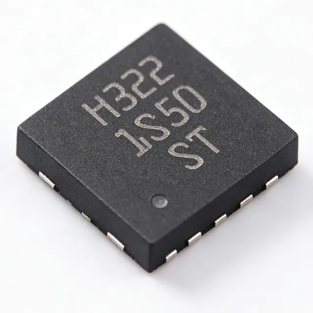
ST1S50PUR - 3A, 18V Synchronous Step-Down Converter | STMicroelectronics
The ST1S50PUR is a high-efficiency, synchronous step-down DC-DC converter from STMicroelectronics, designed to deliver up to 3A of continuous output current from an input voltage range of 4V to 18V. Housed in a compact DFN8 (3x3 mm) package, this device integrates both high-side and low-side power MOSFETs, eliminating the need for an external Schottky diode and simplifying PCB layout. The output voltage is adjustable from 0.8V to VIN, allowing flexibility for a wide range of applications. A synchronous buck converter is a type of DC-DC step-down regulator that uses two active switches (typically MOSFETs) instead of a diode for the low-side element, which significantly improves efficiency, especially at lower output voltages. This architecture is fundamental in power management ICs, where efficiency directly impacts battery life, thermal management, and system reliability. The ST1S50PUR belongs to the family of synchronous step-down converters, which are essential building blocks in modern electronic systems, from portable devices to industrial equipment. Key features of the ST1S50PUR include a fixed 1.5 MHz switching frequency, which allows the use of small, low-cost inductors and capacitors, reducing the overall solution footprint. The device offers a typical efficiency of 90% at 3A load, with a low quiescent current of 1.2 mA in light-load operation. It also features internal soft-start to limit inrush current, overcurrent protection, and thermal shutdown for robust operation. The DFN8 package has an exposed pad for enhanced thermal performance, with a thermal resistance of 40°C/W. The ST1S50PUR utilizes a current-mode control architecture, providing fast transient response and stable operation over a wide range of input and output voltages. The integrated MOSFETs have low RDS(on) (typically 120 mΩ high-side and 80 mΩ low-side), minimizing conduction losses. The device operates over a junction temperature range of -40°C to +150°C, making it suitable for demanding environments. Typical applications include point-of-load (POL) converters for FPGAs, DSPs, and microcontrollers, as well as power supplies for set-top boxes, networking equipment, and industrial control systems. The wide input voltage range also supports 12V and 24V bus systems, making it versatile for various power architectures. When designing with the ST1S50PUR, ensure proper input and output capacitor selection to maintain stability and minimize ripple. The exposed pad should be soldered to a large copper area for effective heat dissipation. The EN pin allows for power sequencing, and the soft-start feature prevents output overshoot during startup.

ST730M50R - 300mA 28V LDO Regulator, 5V Fixed Output | ST | STMicroelectronics
The STMicroelectronics ST730M50R is a 300 mA, 28 V low-dropout (LDO) linear voltage regulator with a fixed 5.0 V output, housed in a 5-pin SOT-23-5 surface-mount package. It accepts an input voltage from 2.5 V to 28 V, delivers up to 300 mA of continuous output current, and exhibits a typical dropout voltage of approximately 600 mV at full load. The regulator draws only 5 microamperes of quiescent current, making it well suited to always-on and battery-powered designs. According to the manufacturer datasheet (document DS13036, revision 5, December 2023), the part embeds current-limit, short-circuit, and thermal-shutdown protection blocks to survive field faults. An LDO (Low-Dropout) linear regulator is a class of voltage regulator that maintains a tightly regulated output voltage even when the input voltage approaches the output voltage - the so-called dropout condition. LDOs sit one rung below the broader linear-regulator family, which itself is a subset of voltage regulators and ultimately of power management ICs (PMICs). Unlike switching converters, LDOs do not introduce switching ripple into the output rail, which is the central reason engineers select them for noise-sensitive analog supply pins. Key differentiating features include the 28 V maximum input rating (well above the common 5 V or 12 V rails), the very low 5 µA quiescent current that preserves standby battery life, and 600 mV typical dropout that lets the LDO regulate cleanly even on depleted battery or under varying load transients. The internal current-limit foldback and 165 °C thermal-shutdown threshold (typical) defend the die against overload and PCB hot-spots. Output voltage accuracy is specified at +/-2 percent over line, load, and temperature. Architecturally the ST730M50R is a PMOS-pass LDO with a high-impedance feedback divider, bandgap reference, and error amplifier. The PMOS topology provides low dropout and inherent short-circuit protection through Rds(on) self-limiting, while the bandgap reference delivers temperature-stable 5 V with low noise density on the output pin. Typical applications include 24 V industrial sensor biasing, after-market automotive accessories (e.g., dashcams and alarms), microcontroller and wireless-module always-on rails, low-power IoT nodes powered directly from 12 V batteries, and post-regulation stages that clean up switching-converter outputs for analog subsections. The wide input range also lets the same part cover both 12 V and 24 V industrial bus systems, simplifying BOM management. Designers should pay close attention to thermal dissipation: at VIN = 24 V, VOUT = 5 V and 300 mA, the device dissipates roughly 5.7 W and requires either a copper-cooling pour or the larger SOT-23-5 land pattern with thermal vias. Use a 1 µF X7R ceramic on the input and a 2.2 µF X7R ceramic on the output placed within a few millimetres of the pins - the part is specified for ESR stability up to several hundred milliohms. This page synthesises distributor pricing, drop-in alternatives, and practical thermal/protection notes drawn from the ST730 datasheet and reference designs - content not assembled on any single manufacturer page.

STA350BW - 2.1-Channel Digital Audio System | STMicroelectronics
The STMicroelectronics STA350BW is a 2.1-channel high-efficiency digital audio system with an integrated digital audio processor, digital amplifier controller, FFX power output stage, and four power outputs in a PowerSSO-36 EPD package. Its documented operating supply range reaches 26 V, with a 30 V absolute maximum rating. The system can deliver 1 x 75 W into 4 Ω with the supply voltage set to 25 V under the manufacturer’s stated conditions. A digital audio system combines signal processing, amplifier control, and power-stage conversion into one integrated device. Within the broader semiconductor hierarchy, the STA350BW belongs to the power-management IC class and specifically serves as a digital Class-D audio amplifier and Sound Terminal. This integration reduces the number of separate blocks required for a compact audio output stage while retaining programmable audio processing. The STA350Bx family provides up to 8 programmable biquads per channel for equalization. Four power outputs support multi-channel and 2.1-channel system configurations. The supplied test condition of VCC = 24 V, f = 1 kHz, fsw = 384 kHz, ambient temperature of 25°C, and RL = 8 Ω provides a defined basis for comparing datasheet specifications; results obtained under different conditions should not be treated as directly equivalent. The device integrates digital audio processing, digital amplifier control, and the FFX output architecture into a single high-power sound-terminal solution. Its four-output architecture provides flexibility for stereo, multi-channel, or subwoofer arrangements, while the digital equalization capability permits channel-specific tonal shaping. The package includes an exposed pad that must be handled according to the manufacturer’s thermal and layout guidance. Typical applications include compact active speakers, multimedia speaker systems, home-theater sound terminals, powered subwoofers, and consumer audio products requiring multiple amplified outputs. In these systems, the integrated processing and output stage can simplify the signal chain compared with a design that uses separate DSP, amplifier-control, and power-amplifier blocks. The 75 W output capability is particularly relevant to compact high-power speaker enclosures. The principal design consideration is thermal management. The exposed pad is integral to heat dissipation and must be connected to a suitable copper area according to the manufacturer datasheet. Designers should also maintain the required input, output, filtering, and decoupling layout, preserve the specified switching conditions, and account for the difference between the 26 V operating range and 30 V absolute maximum rating. This product page consolidates the verified manufacturer specifications, distributor availability information, package details, and engineering guidance for the STA350BW. It also distinguishes directly documented characteristics from parameters that require confirmation from the complete datasheet, helping engineers evaluate thermal design and replacement decisions without inferring unverified compatibility.

STA500 - 30V 3.5A Quad Power Half-Bridge | STMicroelectronics
The STMicroelectronics STA500 is a monolithic quad power half-bridge stage in Multipower BCD technology, rated for a 30 V supply and 3.5 A output in a PowerSO-36 surface-mount package. It combines four configurable half bridges with complementary DMOS output stages, CMOS-compatible logic inputs, and protection for thermal, overvoltage, and undervoltage conditions. A power half-bridge is a switchable power-conversion building block within a bridge amplifier or motor-driver system. Each half bridge uses two complementary switches to drive a load between the supply rail and ground. The STA500 can operate as a dual bridge or, with CONFIG connected to VDD, as a single bridge with doubled current capability. It can also be reconfigured for half-bridge operation in binary mode. This hierarchy places the STA500 among Class D power stages, bridge-driver ICs, and power-management semiconductors. Key features include a 30 V maximum supply rating, 3.5 A output-current capability, 200 mΩ complementary DMOS output resistance, and CMOS-compatible logic inputs. The device also provides output overvoltage and undervoltage protection plus thermal warning and thermal shutdown. These functions make the STA500 suitable for compact Class D audio output stages where multiple switched outputs are required. Technically, the monolithic quad-stage architecture reduces the number of external power devices needed for a multichannel or bidirectional-bridge amplifier. Multipower BCD technology integrates the power output path with control logic in one package. The PowerSO-36 format supports surface-mount assembly while providing a substantial thermal pad for heat transfer into the PCB copper area. Designers should still verify the exact SOA, thermal limits, output-current derating, and pin-level conditions against the manufacturer datasheet. Typical uses include stereo and multichannel audio amplifiers, portable speakers, powered headphones, subwoofer stages, and compact Class D systems. Binary-mode operation can also suit specialized bidirectional or transformer-isolated audio topologies where the application requires half-bridge behavior rather than conventional full-bridge drive. For robust implementation, preserve the datasheet input/output decoupling arrangement, route high-current outputs with minimal loop area, and provide substantial thermal copper under the exposed pad. The STA500 is a 30 V part, so 30 V is a maximum rating rather than a recommended operating margin; transient, supply, and signal limits must be respected. This page consolidates verified manufacturer and distributor information, strict drop-in alternative screening, application guidance, and practical PCB considerations. Because the supplied data does not establish a sufficient set of pin-to-pin replacements, compatibility and lifecycle details are explicitly qualified rather than inferred.
STA505 - 40V 3.5A Quad Half-Bridge Amplifier | STMicroelectronics
The STMicroelectronics STA505 is a 40 V, 3.5 A quad power half-bridge stage in a PowerSO-36 package, intended for Class D audio amplification in mono, stereo, or reconfigured bridge arrangements. It integrates four complementary power half-bridges, configurable operating modes, CMOS-compatible logic inputs, thermal protection, and output overvoltage and undervoltage detection. An audio power half-bridge is one section of a switching amplifier that uses complementary power transistors to drive a load in one current direction. A quad half-bridge can provide two stereo channels, four independent modulation outputs, or another bridge configuration selected by the CONFIG pin. The STA505 is therefore positioned between discrete power-stage design and a complete integrated audio amplifier. Key verified characteristics include a 40 V power-stage rating, a 3.5 A half-bridge current capability, BCDMOS technology, and PowerSO-36 packaging. The device can be used as a dual bridge or reconfigured by connecting CONFIG to VDD for a single-bridge configuration with double current capability. Its binary half-bridge mode is also identified in the manufacturer datasheet. The STA505 is suitable for high-power Class D audio systems, including stereo speaker drives, mono subwoofer amplifiers, compact hi-fi equipment, and external amplifier modules. Compared with a discrete MOSFET output stage, the monolithic quad half-bridge reduces board-level integration effort while retaining configurable drive modes and integrated protection functions. Designers should verify the exact input, output, power, and protection limits in the STMicroelectronics datasheet before layout and power-supply selection. The PowerSO-36 package requires careful thermal planning, low-impedance supply routing, and output-filter design appropriate to the target speaker impedance and switching frequency. This page consolidates the verified manufacturer and distributor information for the STA505, including configuration guidance, application context, and practical design considerations for evaluating the quad half-bridge stage.
STA50513TR - 40V 3.5A Class D Power Half Bridge | STMicroelectronics
STMicroelectronics STA50513TR is a 40 V, 3.5 A quad power half-bridge Class D audio amplifier IC packaged in PowerSO-36. The device provides a monolithic four-half-bridge output stage for efficient audio power amplification, with complementary DMOS outputs and CMOS-compatible logic inputs. It is suitable for compact speaker-driving systems requiring high output current, integrated thermal supervision, and protection against undervoltage conditions. A Class D audio amplifier is a switching power amplifier that uses a pulse-width-modulated output stage to deliver energy to loudspeakers with high efficiency. The STA50513TR belongs to the amplifier IC and power-management semiconductor hierarchy, combining four MOSFET-based half bridges, gate-drive circuitry, logic control, and protection functions. This integration reduces the external component count compared with discrete power-stage designs while preserving efficient audio amplification. Key features include MultiPower BCD technology, a 200 mΩ complementary DMOS output stage, CMOS-compatible logic inputs, thermal protection, a thermal warning output, and output undervoltage protection. The stated 40 V device rating provides headroom for automotive and industrial battery-fed audio systems, while the 3.5 A rating identifies the maximum output-current capability of the integrated power stage. The four-half-bridge arrangement supports bridge-tied speaker configurations and multi-channel audio architectures. The monolithic power stage is designed to minimize external switching hardware while providing gate-drive and protection functions in the same package. BCD technology combines bipolar circuitry, CMOS control logic, and DMOS power transistors on one die, supporting accurate control and efficient power delivery. Input/output pulse-width distortion is specified as a minimum feature of 200 mΩ in the product description, supporting low-loss operation when paired with suitable inductors, speakers, filtering, and thermal management. Typical applications include automotive audio head units, compact hi-fi systems, Bluetooth speaker platforms, multimedia enclosures, soundbars, and powered subwoofer modules. The device is especially relevant where a 24 V vehicle battery or other higher-voltage source must drive low-impedance speakers without using multiple discrete bridge amplifiers. System designers should also account for inductive loads on outputs and preserve the power stage's thermal operating margin. The primary design consideration is heat management. Four integrated half bridges can concentrate substantial dissipation in the PowerSO-36 package, especially when driving low-impedance loads at high output power. PCB copper area, thermal vias, short output paths, correct inductor selection, and protection-network design materially affect reliability. The thermal warning and shutdown functions should be monitored rather than treated as substitutes for adequate board-level cooling. This product page combines the device's stated voltage, current, output-stage, protection, and packaging characteristics with practical application guidance, package-selection limitations, and verified source links. It also distinguishes what can be confirmed for the exact STA50513TR ordering code from parameters that must be obtained from the manufacturer datasheet before schematic release or production qualification.
STA508 - 40V 4.5A Quad Power Half Bridge | STMicroelectronics
The STMicroelectronics STA508 is a 40 V, 4.5 A monolithic quad power half-bridge stage implemented in Multipower BCD technology and packaged in PowerSO-36. It provides four configurable half-bridge outputs that can operate as two full bridges, one full bridge with doubled output-current capability when CONFIG is tied to VDD, or individual half bridges in Binary mode with reduced current capability. A power half bridge is a switching amplifier stage containing two MOSFETs arranged between the supply and ground rails, with one output node at their midpoint. A quad half-bridge IC consolidates four such stages so Class D audio controllers can drive stereo, multi-channel, or bridged speaker systems efficiently. The STA508 is therefore positioned within the hierarchy of Class D audio amplifier IC, power half-bridge, audio output stage, and power management semiconductor. Key verified features include a 40 V maximum power-supply rating, 4.5 A output-current capability, four integrated power half bridges, configurable bridge topology, and Multipower BCD process technology. Configuration flexibility allows the same device organization to support dual-bridge, single-bridge, and Binary half-bridge operation, reducing board-area requirements when a product family needs multiple channel counts. The device is intended to work with an external Class D audio controller rather than directly accept analog audio. The controller generates gate-drive signals, while STA508 supplies the high-current switching path to the speaker outputs. Its BCD construction combines analog control capability with efficient power-device integration, making it suitable for compact, high-power audio systems where board area and channel flexibility matter. Typical applications include stereo Class D amplifiers, multi-channel home audio, active speakers, powered subwoofers, and compact consumer audio products. A 24 V system is specifically shown in the verified web material for an STA508 monoblock amplifier, illustrating use of the device's 40 V supply capability. Thermal and layout design are critical because the PowerSO-36 package and external heatsink must dissipate the power-stage loss. The power and ground pins, output nodes, controller interface, and decoupling network should follow the manufacturer datasheet layout exactly. Keep high-current loops compact and provide adequate copper and heatsinking; otherwise output-current capability can be limited by junction temperature before the electrical rating is reached.
STA540SAN - 4x10W Class-AB Audio Amplifier | STMicroelectronics
The STMicroelectronics STA540SAN is a 4 x 10 W dual/quad power amplifier for high-quality sound applications. The device contains four single-ended, class-AB audio amplifiers in a Clipwatt15 package and can operate as a stereo pair or as four independent amplifier channels. Its headline specifications are four integrated amplifier channels, 10 W per channel, and an 8 V to 22 V supply range. Each amplifier includes integrated short-circuit protection, thermal protection, and diagnostic functions. Two amplifiers can be paired for applications requiring higher power output. The STA540SAN belongs to the power-amplifier IC hierarchy, where an audio amplifier drives loudspeakers or other low-impedance loads while providing voltage gain and output-current capability. Class-AB operation provides a practical balance between conduction efficiency and low crossover distortion for conventional consumer and industrial audio systems. The single-ended amplifier architecture is suitable for compact designs where a bridge-tied configuration, external bootstrap capacitors, or Boucherot cells are not required. Key features include four single-ended outputs, a 2-channel stereo or 4-channel quad operating mode, integrated short-circuit and thermal protection, diagnostic functions, and a reduced external-component count. The manufacturer datasheet states that no bootstrap capacitors or Boucherot cells are required. The Clipwatt15 package is intended for through-hole or board-level audio power designs and provides a practical thermal and assembly solution for amplifiers operating near the device's rated output capability. The STA540SAN is suitable for stereo receivers, compact audio systems, television or monitor amplification, multimedia speakers, industrial audio equipment, and other applications using 4-ohm or 8-ohm speakers. When selecting the supply voltage, ensure that the amplifier has sufficient headroom for the chosen load and that the PCB provides adequate copper area and thermal dissipation. The standby control and diagnostic functions should be checked against the system-level requirements before production design. This product page combines the verified manufacturer and distributor information with practical selection guidance, pricing-status notes, and conservative drop-in replacement analysis. It identifies where a same-package replacement is supported by the available cross-reference data and where pinout and electrical verification remains essential.
STA575 - 100W Stereo BASH Power Amplifier | STMicroelectronics
The STMicroelectronics STA575 is a 100+100 W stereo BASH power amplifier designed for use with the STABP01 digital processor. It delivers 80+80 W into 4 or 8 ohm loads at 0.5% total harmonic distortion and is available in the 27-Flexiwatt vertical power package. The device uses a mono-chip bridge stereo amplifier architecture with high-dynamic preamplifier input stages, external programmable feedback, compressors, and AC-coupled inputs. The STA575 is an integrated audio power module within the broader amplifier IC, audio amplifier, and Class AB amplifier hierarchy. Class AB amplifiers combine transistor conduction for improved linearity with lower distortion than many switching audio power stages. In the BASH architecture, the STABP01 supplies digital control and signal-processing functions while the STA575 provides the high-power analog output stage and speaker drive capability. Key features include 100+100 W output power into 4 or 8 ohms at 10% THD, 80+80 W output power at 0.5% THD, stereo operation, high-dynamic preamplifier inputs, external programmable feedback, integrated compressor functions, and AC-coupled input coupling. The 27-pin Flexiwatt vertical package is intended for audio power amplifier designs requiring substantial output current and thermal management. The device is intended for stereo speaker systems, compact hi-fi equipment, multimedia enclosures, powered speakers, and other Class AB audio products. The manufacturer datasheet identifies the BASH architecture and the electrical operating limits that determine speaker impedance, supply voltage, thermal design, and distortion performance. Designers should use the complete datasheet for pin assignment, recommended application circuitry, protection requirements, and maximum ratings. Because this is a high-power analog module, PCB layout and heat sinking are as important as signal selection. Keep high-current speaker paths short and wide, use the recommended input and feedback networks, decouple the supply rails close to the device, and validate thermal performance at the intended output power. A nominal 100 W rating does not eliminate the need for an adequate copper area, thermal interface, enclosure airflow, or speaker-load verification. This page combines the verified STMicroelectronics and distributor descriptions with practical engineering guidance. It is intended to help engineers identify the correct function, package, power class, datasheet, and design constraints while avoiding unsupported substitute claims or fabricated electrical details.
STA8600A - High-Performance Audio Amplifier IC | STMicroelectronics
The STA8600A is a high-performance audio amplifier integrated circuit from STMicroelectronics, designed for automotive and consumer audio systems. It delivers up to 4 x 50W output power into 4Ω loads, with a wide supply voltage range of 6V to 18V. The device is housed in a 36-pin PowerSO package, providing excellent thermal performance for high-power applications. An audio amplifier is an electronic device that increases the amplitude of audio signals, driving speakers or transducers. It is a critical component in the audio signal chain, converting low-power audio signals into high-power outputs suitable for loudspeakers. Audio amplifiers are classified into classes (A, B, AB, D) based on their operating principles and efficiency. The STA8600A is a Class AB amplifier, offering a balance between linearity and efficiency, making it suitable for high-fidelity audio reproduction. Key features of the STA8600A include a high signal-to-noise ratio of 100 dB, low total harmonic distortion of 0.01% at 1 kHz, and a wide operating temperature range of -40°C to +105°C. The device integrates multiple protection features, including overcurrent, overtemperature, and short-circuit protection, ensuring reliable operation in demanding environments. The PowerSO package with exposed pad enhances heat dissipation, allowing continuous high-power output without external heatsinks in moderate conditions. The STA8600A utilizes a complementary bipolar output stage with a precision bias circuit, achieving low crossover distortion and stable quiescent current. The device supports multiple output configurations, including stereo and quad-channel modes, providing flexibility for various system designs. Its high PSRR of 80 dB minimizes power supply noise, ensuring clean audio output even with noisy supply rails. Typical applications include car audio head units, external amplifiers, home theater systems, and active speakers. The wide supply voltage range makes it compatible with both 12V automotive systems and 18V consumer electronics. The integrated protection features reduce external component count, simplifying PCB design and improving system reliability. When designing with the STA8600A, ensure adequate PCB copper area for thermal dissipation, especially when driving low-impedance loads at high power. The exposed pad must be soldered to a large ground plane to achieve the specified thermal resistance. Proper decoupling on the supply pins is essential to maintain stability and minimize distortion.
STA8610A - High-Performance Audio Amplifier IC | STMicroelectronics
The STA8610A is a high-performance audio amplifier integrated circuit from STMicroelectronics, designed for automotive and consumer audio systems. It delivers up to 4 x 50W output power into 4Ω loads, with a wide supply voltage range of 6V to 18V. The device is housed in a 36-pin PowerSO-36 package, providing excellent thermal performance for high-power applications. An audio amplifier is an electronic device that increases the amplitude of audio signals, driving speakers or headphones with sufficient power and fidelity. In the signal chain, the audio amplifier sits between the preamplifier (or DAC) and the speakers, converting low-level audio signals into high-power outputs. It is a critical component in the audio system hierarchy, which includes sources (e.g., CD players, smartphones), preamplifiers, amplifiers, and transducers. The STA8610A belongs to the class of analog power amplifiers, specifically designed for multi-channel applications. Key features of the STA8610A include a high output power of 4 x 50W at 10% THD, a low quiescent current of 120mA, and a wide operating temperature range of -40°C to +105°C. The device integrates short-circuit protection, thermal shutdown, and standby/mute functions, ensuring robust operation in demanding environments. Its high efficiency and low distortion make it suitable for high-fidelity audio reproduction. The STA8610A utilizes a complementary MOS (CMOS) output stage, providing high current capability and low output impedance. The device features a differential input stage for improved noise rejection and a sophisticated bias circuit to minimize crossover distortion. The PowerSO-36 package with exposed pad enhances heat dissipation, allowing continuous operation at high power levels without external heatsinks in moderate conditions. Typical applications include car audio head units, home theater systems, and active speaker systems. In automotive applications, the STA8610A's wide supply range and robust protection features ensure reliable performance under varying battery conditions. In home theater, its multi-channel capability simplifies the design of surround-sound amplifiers. When designing with the STA8610A, ensure adequate PCB copper area for thermal management, especially when driving low-impedance loads at high power. The standby and mute pins allow for power management and pop-noise reduction during power-up and shutdown sequences.

STCMB1 - TM PFC + LLC Combo Controller 800V | STMicro
The STMicroelectronics STCMB1 is a combination transition-mode (TM) Power Factor Correction (PFC) controller and high-voltage double-ended LLC resonant half-bridge controller integrated in a single chip, supplied in a 20-pin SO (SO20W) package. According to the manufacturer datasheet, the device targets SMPS adapters and open-frame power supplies with universal-mains input and high-voltage DC output, where it implements both the front-end PFC pre-regulator and the downstream resonant converter with a glue-logic supervisor in one IC. A TM PFC controller (transition-mode PFC, also known as critical-conduction-mode PFC) is a power-factor-correction topology that forces the boost inductor current to reach zero before each switching cycle is re-triggered. Compared with continuous-conduction-mode (CCM) PFC, it reduces switching losses and enables the use of smaller magnetics, making it popular in adapters up to a few hundred watts. An LLC resonant half-bridge is a soft-switching DC-DC topology that achieves zero-voltage switching on the primary FETs and zero-current switching on the secondary rectifiers, delivering high efficiency at high switching frequency with low EMI. The STCMB1 combines both stages plus 800 V start-up and X-cap discharge, removing the need for a separate standby controller. Key features of the STCMB1 include 800 V high-voltage start-up with integrated input voltage sensing, active X-cap discharge circuitry (IEC 62368-1 and UL Demko certified) for reduced standby power, a switching frequency of approximately 500 kHz for the LLC stage, independent debug mode for both PFC and LLC, and an internal 2.5 V transconductance reference. The 800 V high-voltage section supports universal mains (90-265 V AC) and over-voltage transients without an external depletion-mode MOSFET or auxiliary winding, simplifying the front-end biasing. The X-cap discharge block eliminates the bleeder resistors traditionally required to meet safety standards for input capacitor discharge time after AC removal. The regulation loop uses a transconductance amplifier with an internal 2.5 V reference and a typical gain-bandwidth product of 1 MHz, providing the PFC output voltage regulation and LLC output voltage regulation with two external compensation networks. The glue logic coordinates soft-start, brown-in/brown-out, fault handling, and burst-mode entry across the two stages, so designers do not need to interlock two separate controllers manually. Wide-bandgap compatibility (GaN and super-junction silicon) is supported through the high-side driver output structure. Typical applications of the STCMB1 include 90 W to 300 W USB-PD adapters, laptop power supplies, LED TV power boards, all-in-one PC supplies, and any high-density AC-DC converter where efficiency above 90 percent, low standby power (below 75 mW via X-cap discharge), and reduced BOM count are design priorities. The 20-pin SO wide-body (SO20W) package provides sufficient creepage for primary-side high-voltage pins and adequate thermal performance for adapters operated in enclosed plastic housings. When designing with this IC, layout the PFC inductor and the LLC resonant tank so that their high-current loops do not share a common ground return with the small-signal analog ground of the TM PFC E/A. Designers should also ensure the X-cap discharge path is intact for IEC 62368-1 compliance and place the bootstrap diode close to the high-side driver pin to avoid shoot-through during LLC start-up transients. This page synthesizes distributor stock signals, pricing, drop-in alternatives, and practical design notes not found in the manufacturer datasheet, providing engineers with a consolidated technical reference for SMPS adapter development.
STEF512PUR - Dual eFuse 5V/12V 3A Hot-Swap | STMicroelectronics
The STMicroelectronics STEF512PUR is an integrated dual electronic fuse (eFuse) that protects downstream circuitry from overcurrent and overvoltage events in applications requiring hot-swap operation and inrush current control. The device embeds two independent high-side load switches — one optimized for 5 V rails and one for 12 V rails — each rated up to 3 A continuous current in a 10-pin QFN (2 mm x 3 mm) package. Each channel integrates a low-RDS(on) power FET that minimizes voltage drop from the main supply to the load during normal operation, plus two analogue control loops that clamp output voltage and limit input current independently. An electronic fuse (eFuse) is a solid-state replacement for a traditional thermal fuse or PTC, offering resettable, programmable protection with fast fault response. It belongs to the broader family of hot-swap controllers and current regulators within power-management ICs (PMICs). The eFuse architecture allows precise user-adjustable startup behavior via external soft-start capacitors and current-limit thresholds via sense resistors, eliminating the need for bulky mechanical fuses in space-constrained designs. Key features include independent fault timers, thermal shutdown, UVLO and OVLO protection per channel, a Fault flag output for system-level diagnostics, and adjustable slew-rate control. Each eFuse channel operates independently, allowing the 5 V and 12 V rails of a system to be protected, sequenced, and monitored separately without external coordination logic. The integrated MOSFETs drastically reduce BOM count compared to discrete hot-swap solutions built from FETs, op-amps, and sense resistors. Typical applications include hot-swap insertion in rack-mounted servers, SSD and HDD power-rail protection, set-top box and consumer-electronics load switches, USB Type-C VBUS current limiting, and industrial 24 V backplane protection when paired with a pre-regulator. The dual-rail architecture is particularly efficient in ATX-style PC subsystems and small-form-factor systems that need both 5 V standby and 12 V main rail protection. A critical design consideration is the choice of soft-start capacitor, which sets the inrush-current profile and the fault-timer timeout. Engineers should also account for the package's thermal resistance — at full 3 A per channel, sufficient copper pour is required to keep junction temperature within the datasheet limits. This page synthesizes distributor pricing, drop-in alternatives, and practical design notes not found in the manufacturer datasheet alone.
STGAP1BS - 4A Galvanically Isolated Single Gate Driver | STMicroelectronics
The STGAP1BS is a galvanically isolated single gate driver from STMicroelectronics, designed to drive high-power IGBTs and SiC MOSFETs in industrial and automotive applications. It provides a 4A sink/source peak output current and features a 4 kV galvanic isolation barrier, making it suitable for motor drives, power supplies, and renewable energy inverters. The device is available in a wide-body SO-8W package, which offers a compact footprint while maintaining high isolation voltage. A gate driver is a power amplifier that accepts a low-power input from a controller IC and produces a high-current drive output to control the gate of a power transistor. In the hierarchy of power electronics, a gate driver sits between the control stage (microcontroller or DSP) and the power stage (IGBT or MOSFET), ensuring fast and reliable switching. The STGAP1BS integrates a galvanic isolation barrier, which separates the input and output grounds, protecting the low-voltage control circuitry from high-voltage transients and ground loops. Key features of the STGAP1BS include a 4A peak output current, 4 kV galvanic isolation, 100 V/ns common-mode transient immunity (CMTI), and a wide supply voltage range from 4.5V to 18V on the output side. The device also features a Miller clamp function to prevent spurious turn-on during high dv/dt events, and a desaturation protection input for overcurrent detection. These features make it ideal for driving SiC MOSFETs and IGBTs in high-frequency, high-efficiency power converters. The STGAP1BS uses STMicroelectronics' proprietary galvanic isolation technology, which provides robust isolation with low propagation delay (typically 75 ns) and tight part-to-part matching. The device supports both bipolar and unipolar supply configurations, allowing flexible design for various gate drive requirements. The wide-body SO-8W package ensures adequate creepage and clearance distances for 4 kV isolation, meeting IEC 60747-17 requirements. Typical applications include motor drives for industrial automation, solar inverters, uninterruptible power supplies (UPS), and electric vehicle (EV) charging stations. The STGAP1BS is also suitable for welding equipment and induction heating systems, where high reliability and fast switching are critical. When designing with the STGAP1BS, ensure proper PCB layout to minimize parasitic inductance in the gate drive loop. Use a low-ESR capacitor close to the VCC and GND pins to supply the high peak currents. The Miller clamp pin should be connected to the gate of the power transistor with a short, low-inductance trace to effectively suppress dv/dt-induced turn-on.
STGAP2HSA - 4A Galvanically Isolated Gate Driver | STMicroelectronics
The STGAP2HSA is a galvanically isolated single-channel gate driver from STMicroelectronics, designed to drive high-power IGBTs and SiC MOSFETs in industrial and automotive applications. It delivers up to 4A of peak output current with a wide supply voltage range of 3V to 18V on the primary side and 4.5V to 18V on the secondary side. The device features a 100V/ns common-mode transient immunity (CMTI) and a propagation delay of 75ns, ensuring robust performance in noisy power environments. A galvanic isolation barrier is a critical safety feature in power electronics that electrically separates the low-voltage control circuitry from the high-voltage power stage, preventing ground loops and protecting sensitive logic. The STGAP2HSA uses a capacitive isolation technology that provides reinforced isolation up to 6kV, meeting stringent safety standards for industrial motor drives and solar inverters. This isolation barrier is essential in applications where the control and power grounds are at different potentials, such as in half-bridge or full-bridge topologies. Key features of the STGAP2HSA include a 4A sink/source peak current, a 75ns propagation delay, and a 100V/ns CMTI. The device also offers a programmable dead time function, a shutdown pin for fault protection, and a separate output pin for Miller clamp, which prevents spurious turn-on of the power switch during high dv/dt events. The wide supply voltage range and rail-to-rail output make it compatible with a variety of gate drive circuits. The STGAP2HSA is built using STMicroelectronics' proprietary galvanic isolation technology, which uses a high-voltage capacitor to transfer signals across the isolation barrier. This architecture achieves low power consumption and high reliability, with a typical quiescent current of 1.5mA on the primary side. The device is available in a compact SO-8 package, which simplifies PCB layout and reduces board space in space-constrained designs. Typical applications include industrial motor drives, solar inverters, uninterruptible power supplies (UPS), and electric vehicle (EV) charging systems. In motor drives, the STGAP2HSA drives the IGBTs in the inverter stage, providing fast and reliable switching to minimize losses. In solar inverters, it drives the SiC MOSFETs in the boost converter, enabling high-frequency operation and improved efficiency. When designing with the STGAP2HSA, it is important to ensure proper PCB layout to minimize parasitic inductance in the gate drive loop. The Miller clamp output should be connected to the gate of the power switch to prevent false turn-on. Additionally, the dead time programming pin should be configured with an external resistor to set the desired dead time for the application.
STGAP2SA - 4A Galvanic Isolated Single Gate Driver | STMicroelectronics
The STGAP2SA is a galvanic isolated single gate driver manufactured by STMicroelectronics, designed to drive wide-bandgap power switches such as SiC MOSFETs and GaN HEMTs. It provides a 4A sink/source peak output current and features a 4 kV galvanic isolation barrier, making it suitable for high-voltage and high-reliability applications. The device is available in a narrow-body SO-8 package, which is compact and suitable for space-constrained designs. A galvanic isolated gate driver is a type of gate driver IC that provides electrical isolation between the input control side and the output power stage. This isolation is critical in applications where the power stage operates at high voltages, as it protects the low-voltage control circuitry from transients and ground potential differences. The STGAP2SA belongs to the category of isolated gate drivers, which are essential components in power electronics systems such as motor drives, power supplies, and inverters. Key features of the STGAP2SA include a 4A peak output current, a wide supply voltage range of 3V to 18V on the output side, and a 4 kV galvanic isolation rating. The device also offers a propagation delay of 75 ns, which is critical for high-frequency switching applications. The input side operates from 3V to 18V, and the device includes a Miller clamp function to prevent false turn-on of the power switch during high dv/dt events. The STGAP2SA utilizes STMicroelectronics' proprietary galvanic isolation technology, which provides robust isolation performance with high common-mode transient immunity (CMTI) of 100 V/ns. This ensures reliable operation in noisy environments. The device also features an under-voltage lockout (UVLO) on both the input and output sides, protecting the power switch from insufficient gate drive voltage. Typical applications for the STGAP2SA include motor drives, industrial power supplies, solar inverters, and electric vehicle (EV) charging systems. Its high output current and fast propagation delay make it suitable for driving SiC MOSFETs and GaN HEMTs in high-frequency power converters. The device is also used in welding equipment and induction heating systems where high reliability and isolation are required. When designing with the STGAP2SA, it is important to ensure proper PCB layout to minimize parasitic inductance and maintain isolation creepage distances. The Miller clamp feature should be utilized in applications with high dv/dt to prevent unintended turn-on. Additionally, the UVLO thresholds should be considered to ensure the gate driver operates within the specified voltage range.

STGAP4S - 4-Channel Isolated Gate Driver | STMicroelectronics
The STGAP4S is a 4-channel isolated gate driver from STMicroelectronics, designed for driving IGBTs and MOSFETs in high-voltage applications. It provides four independent galvanically isolated channels, each capable of delivering up to 4 A peak output current, making it suitable for three-phase inverters, motor drives, and industrial power supplies. The device operates from a supply voltage range of 4.5 V to 18 V on the logic side and 4.5 V to 18 V on the driver side, with a common-mode transient immunity (CMTI) of 100 V/ns, ensuring robust operation in noisy environments. An isolated gate driver is a type of gate driver that provides electrical isolation between the control circuitry and the power stage, protecting low-voltage logic from high-voltage transients and ground loops. It is a critical component in power electronics, enabling safe and reliable switching of power semiconductors. The STGAP4S belongs to the category of isolated gate drivers, which are part of the broader family of gate drivers, power management ICs, and semiconductor devices. Key features of the STGAP4S include a 4 A peak output current per channel, a wide supply voltage range, and a propagation delay of 100 ns. It also features an interlock function to prevent cross-conduction, a dedicated enable pin for each channel, and a fault output for system monitoring. The device is available in a 36-pin SSOP package, offering a compact solution for multi-channel gate drive applications. The STGAP4S utilizes STMicroelectronics' galvanic isolation technology, providing reinforced isolation up to 6 kV. The device includes a Miller clamp on each channel to prevent spurious turn-on of the power switch, and a desaturation protection feature for overcurrent detection. The architecture ensures high noise immunity and reliable operation in harsh industrial environments. Typical applications include motor drives, three-phase inverters, uninterruptible power supplies (UPS), and industrial power supplies. The STGAP4S is also suitable for renewable energy systems such as solar inverters and wind turbine converters. Its high CMTI and low propagation delay make it ideal for high-frequency switching applications. When designing with the STGAP4S, it is important to ensure proper PCB layout to minimize parasitic inductance and maintain signal integrity. The device requires careful attention to the isolation barrier and creepage distances to meet safety standards. Additionally, the supply decoupling should be implemented with low-ESR capacitors close to the VCC and GND pins.
STGIPS20C60-H - 600V 20A 3-Phase IGBT IPM | STMicroelectronics
The STMicroelectronics STGIPS20C60-H is a 600 V, 20 A three-phase IGBT Intelligent Power Module (IPM) from the SLLIMM (Small Low-Loss Intelligent Molded Module) family, integrating gate drivers and short-circuit rugged trench-gate IGBTs in a 25-pin PowerDIP module measuring 0.993 inch (25.23 mm) wide. It is designed as a compact, drop-in inverter stage for variable-frequency drives and is rated for 600 V collector-emitter blocking with 20 A continuous phase current, plus an integrated bootstrap diode network, undervoltage lockout, and an on-board comparator for fault/over-current sensing via an external shunt resistor. What is an Intelligent Power Module (IPM)? An IPM is a power semiconductor module that integrates the power switches (here: IGBTs), their gate drivers, and protection features (UVLO, short-circuit, fault output) into a single isolated package. IPMs sit in the power management hierarchy between discrete IGBT/MOSFET inverter stages and higher-level integrated motor-drive modules, simplifying PCB design and shortening time-to-market for three-phase motor control applications such as HVAC compressors, washing-machine pumps, and small industrial inverters. Key features include 600 V short-circuit rugged IGBTs with trench-gate field-stop technology for low VCE(sat) and soft switching, a built-in shunt-style comparator with internal Vref and external CIN pin for hardware over-current protection, undervoltage lockout on all six driver channels, an open-drain fault output, and interlock logic that prevents shoot-through. The molded 25-PowerDIP package provides reinforced insulation and a thermally conductive substrate that simplifies heatsink attachment versus discrete through-hole designs. Typical applications include three-phase motor drives for white goods (washing machines, refrigerators, dishwasher pumps), low-power industrial variable-frequency drives (VFDs) up to about 1.5 kW, fan and compressor inverters for HVAC, and small servo pumps. The IPM's 20 A rating makes it suitable for 230 V AC mains-fed systems driving motors in the 0.37-1.1 kW range. When designing with this device, route the bootstrap capacitors close to pins U, V, W and ensure the comparator CIN pin is filtered to avoid nuisance trips. The internal Vref is non-adjustable, so over-current threshold is set by the external shunt resistor value only.

STLED316SMTR - 6-Digit LED Controller w/ Key Scan, SO-24 | STMicroelectronics
The STMicroelectronics STLED316SMTR is a serial-interfaced 6-digit LED controller with integrated key-scan, designed to drive 7-segment displays through a compact 3-wire SPI-compatible interface. It provides 14 constant-current sink outputs (8 segment lines + 6 digit lines) with 40 mA per-segment drive capability, while a 2x2 key-scan matrix supports up to 4 key inputs. The part operates from a 4.5 V to 5.5 V supply (3 V LED front-panel applications) and is offered in a 24-pin SO-24 small-outline surface-mount package with tape-and-reel packaging for high-volume assembly. What is an LED display controller? An LED display controller (sometimes called an LED driver or display bias IC) is an interface device that sits between a microcontroller and a multiplexed 7-segment or dot-matrix LED panel. It receives display data over a low-pin-count serial bus (SPI, I2C, or proprietary) and re-drives each segment at the correct duty cycle, freeing the host MCU from software multiplexing. In the broader taxonomy, LED display controllers sit beneath LED Drivers -> Power Management -> Power & Interface ICs, and they are distinct from simple LED current sinks because they integrate the timing, brightness, and key-scan logic required for human-machine interface (HMI) panels. Key features of the STLED316SMTR include 14 open-drain segment/digit outputs rated at 40 mA continuous, integrated 3-wire serial interface (clock, data, strobe) compatible with SPI mode 0, hardware key-scan with on-chip debounce, low standby current to support battery-backed panels, and a wide industrial operating temperature range. The device is also designed for minimum external BOM - only the segment current-setting resistor and decoupling caps are required, allowing very compact front-panel PCBs. Typical applications include white-good front panels (washing machines, microwaves, ovens), industrial control HMIs, point-of-sale (POS) terminals, audio equipment displays, instrument cluster readouts, and any 6-digit or smaller 7-segment user interface requiring keypad scanning. With 8 segment + 6 digit outputs the controller can drive a 6-digit 7-segment display plus decimal points, or up to 8 separate status LEDs. When designing with the STLED316SMTR, observe the absolute maximum segment current rating and choose the external RSET resistor accordingly. Ensure the 3-wire interface timing matches SPI mode 0 (CPOL=0, CPHA=0) of the host MCU, and place the decoupling capacitor as close as possible to VDD to suppress key-scan glitches during display multiplexing. This page synthesises distributor pricing, parametric comparison with same-brand and cross-brand drop-in alternatives, and practical design notes that complement - but do not replace - the official STMicroelectronics datasheet.