XC7K325T-1FFG900CES vs XC7K325T-2FFG900I موازنہ
تفصیلی ساتھ ساتھ موازنہ از XC7K325T-1FFG900CES بذریعہ AMD اور XC7K325T-2FFG900I بذریعہ AMD. اہم خصوصیات، برقی پیرامیٹرز، پیکیجنگ، لائف سائیکل اسٹیٹس، قیمتوں اور دستیابی کا موازنہ کریں تاکہ آپ کی ڈیزائن ضروریات کے لیے بہترین کمپوننٹ کا تعین ہو سکے۔

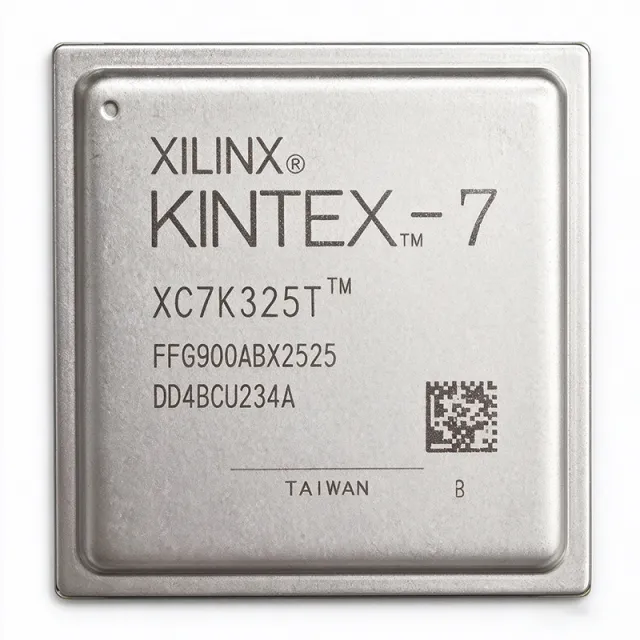
خصوصیات کا موازنہ
| پیرامیٹر | XC7K325T-1FFG900CES | XC7K325T-2FFG900I |
|---|---|---|
| برانڈ | AMD | AMD |
| زمرہ | FPGA & CPLD | FPGA & CPLD |
| لائف سائیکل کی حالت | فعال | فعال |
| اسٹاک کی حالت | — | In Stock |
| فی یونٹ قیمت (USD) | — | $65.00 |
| Device Type | Kintex-7 Field Programmable Gate Array (FPGA) | — |
| Programmable Logic Cells | 326080 cells | — |
| Configurable Logic Blocks | 25475 CLBs | — |
| Internal Memory | 16404480 bits | — |
| User I/O | 500 I/O | 500 |
| Maximum Clock Figure | 1098 MHz | — |
| High-Speed Transceivers | 16 transceivers | — |
| Speed Grade | -1 | -2 |
| پیکیج | 900-BBGA FCBGA, FFG900 | 900-BBGA, FCBGA |
| Ball Count | 900 balls | — |
| Programmable Logic Type | CMOS FPGA | — |
| ماؤنٹنگ ٹائپ | Surface mount | Surface Mount |
| Series | Kintex-7 | — |
| Configuration | FPGA configuration bitstream | — |
| Logic Resources | Programmable logic, block RAM, DSP, I/O, clocking, and GTX transceiver resources | — |
| Package Pinout Reference | Kintex-7 package device pinout files and UG475 | — |
| Operating Voltage | [DATA_NEEDED: core and I/O operating voltage] | — |
| آپریٹنگ درجہ حرارت رینج | [DATA_NEEDED: ES suffix temperature range] | — |
| I/O Standard | [DATA_NEEDED: supported I/O standards] | — |
| RoHS Compliance | unknown | — |
| REACH Compliance | unknown | — |
| Family | — | Kintex-7 |
| Logic Cells | — | 326080 |
| Block RAM | — | 16404480 bits |
| DSP Slices | — | 840 |
| Temperature Grade | — | Industrial (-40°C to +100°C) |
| Process Technology | — | 28nm |
| Core Voltage (VCCINT) | — | 1.0V |
| I/O Standards | — | LVCMOS, LVDS, HSTL, SSTL |
| Transceivers | — | 16 (GTX) |
| PCIe Support | — | Gen3 |
| RoHS اسٹیٹس | — | Compliant |