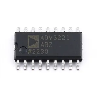
DG409DY+ - Dual 4:1 CMOS Analog Multiplexer | Analog Devices
MPN: DG409DY+ ✓ فعالDG409DY+ جائزہ
An analog multiplexer is an interface IC that connects multiple analog signal paths to a shared output while preserving the selected signal. The DG409DY+ belongs to the CMOS analog multiplexer hierarchy, where four channels and two switch circuits provide bidirectional signal routing for differential or paired single-ended measurements. Its differential 4:1 organization makes it more appropriate than an 8:1 single-ended multiplexer when a system must preserve two related signals together.
Key features include two 4:1 analog switch circuits, maximum on-resistance of 100 ohm, and a 16-SOIC package. According to the manufacturer product page, the redesigned DG408 and DG409 devices provide guaranteed matching between channels of 8 ohm maximum and signal-range flatness of 9 ohm maximum. These channel-matching and flatness characteristics help minimize errors when different input sources feed downstream conversion or measurement circuitry.
The DG409 architecture uses monolithic CMOS switches and TTL/CMOS-compatible control inputs, allowing microprocessor, microcontroller, or logic-level addressing. The mux provides low on-resistance in either signal direction, making the selected channels suitable for bidirectional routing. Designers should still account for switch resistance, off-channel leakage, supply limits, settling behavior, and the analog signal range when determining whether the architecture meets an application's accuracy and bandwidth targets.
Typical applications include differential sensor acquisition, automated test equipment, data acquisition systems, sample-and-hold networks, signal routing for measurement front ends, and multiplexed control paths. The DG409DY+ is particularly useful when several sensors or test nodes must be selected without duplicating a complete analog front end. Its two independent 4:1 sections also permit simultaneous selection of two related channels.
For layout, place the selected source and destination traces close to the device and route them away from high-current switching nodes. Use a continuous ground plane, minimize connector stubs, and provide local bypass capacitance on the supply pins. Confirm the power polarity and maximum supply voltage against the manufacturer datasheet before connecting the part.
This product page combines the DG409DY+ architecture, verified package information, pin-compatible alternatives, application guidance, and practical layout considerations to support faster component selection and board-level implementation.
کے لیے ڈراپ اِن متبادل DG409DY+ — یکساں پیکیج، پن سے پن مطابقت پذیر۔ مختلف پیکیج والے پرزے جن کے لیے PCB دوبارہ کام درکار ہو، شامل نہیں ہیں۔
DG409DY-T1-E3
✅ ڈراپ-اِن📋 حوالہ جاتی متبادل (کیٹلاگ میں نہیں)
DG409DY-T1
✅ ڈراپ-اِن📋 حوالہ جاتی متبادل (کیٹلاگ میں نہیں)
DG409DYZ-T
✅ ڈراپ-اِن📋 حوالہ جاتی متبادل (کیٹلاگ میں نہیں)
ADG409BRZ-REEL
✅ ڈراپ-اِن📋 حوالہ جاتی متبادل (کیٹلاگ میں نہیں)
ADG409BRZ-REEL7
✅ ڈراپ-اِن📋 حوالہ جاتی متبادل (کیٹلاگ میں نہیں)
DG409DY
✅ ڈراپ-اِن📋 حوالہ جاتی متبادل (کیٹلاگ میں نہیں)
DG409DY+ تفصیلات
| Switch Configuration | 2 circuits, each 4:1 |
| Multiplexer Architecture | Dual differential 4:1 CMOS analog multiplexer |
| On-Resistance | 100 ohm maximum |
| Channel Matching | 8 ohm maximum |
| Flatness Over Signal Range | 9 ohm maximum |
| Signal Direction | Bidirectional |
| Control Interface | TTL/CMOS-compatible |
| پیکیج | 16-lead SOIC |
| Lead Count | 16 leads |
| ماؤنٹنگ ٹائپ | Surface mount |
| RoHS Compliance | unknown |
| REACH Compliance | unknown |
DG409DY+ 16-lead soic پن کنفیگریشن گائیڈ
DG409DY+ (16-lead soic پیکیج) کے لیے پن کنفیگریشن۔ پن نمبرنگ، فنکشنز اور کنکشن ڈایاگرامز مینوفیکچرر کے ڈیٹا شیٹ میں بیان کیے گئے ہیں۔ درست فٹ پرنٹ اور سولڈرنگ رہنما ہدایات کے لیے اسی سے رجوع کریں۔

کے لیے تفصیلی پن آؤٹ ڈیٹا دستیاب نہیں DG409DY+.
رجوع کریں ڈیٹا شیٹ مکمل پن کنفیگریشن کے لیے۔
عام استعمالات
DG409DY+ کے لیے موزوں ہے 6 ایپلیکیشنs: Differential Sensor Acquisition, Automated Test Equipment, Multichannel Data Acquisition, Sample-and-Hold Signal Selection, Instrument Signal Routing, Programmable Control Monitoring.
Differential Sensor Acquisition
The DG409DY+ fits differential sensor acquisition because its two independent 4:1 CMOS switch sections can select paired signals while preserving their relationship. Each section routes one of four inputs to a shared output, allowing multiple sensor pairs to share one amplifier and converter chain. The 100 ohm maximum on-resistance must be included when calculating sensor loading, amplifier bias current, noise, and settling time. Channel matching of 8 ohm maximum helps reduce differential gain or offset error when comparing switched channels, while flatness of 9 ohm maximum limits signal-dependent insertion-resistance variation. Use short protected traces and confirm that the sensor output remains within the mux's specified analog signal range.
تجویز کردہ
Automated Test Equipment
The DG409DY+ is useful in automated test equipment when a controller must route several test nodes to a common measurement amplifier or instrument input. Two 4:1 sections provide eight selectable source positions when used as paired differential routes, or four independent differential routes. The 100 ohm maximum on-resistance adds series impedance that can affect high-impedance sources and amplifier settling, so timing should include the selected switch path. The guaranteed 8 ohm maximum channel matching and 9 ohm maximum flatness are particularly useful when comparisons between test channels depend on repeatable resistance. Place the mux close to the instrument front end and keep digital address traces away from the analog inputs.
تجویز کردہ
Multichannel Data Acquisition
The DG409DY+ supports multichannel data acquisition by placing two 4:1 analog switches ahead of shared downstream conversion resources. Eight source channels can be presented to two common outputs when both sections are addressed in parallel, reducing the need for duplicated analog front ends. Because the 100 ohm maximum on-resistance contributes directly to source impedance, the selected sensor or divider must be able to drive the resulting load without excessive gain error. TTL/CMOS-compatible control logic allows direct addressing from a microcontroller or system controller. Firmware should mask or settle each channel before conversion, and the PCB should provide quiet return paths for both analog outputs and the device ground.
تجویز کردہ
Sample-and-Hold Signal Selection
The DG409DY+ can select one of four signals in each circuit for a downstream sample-and-hold stage, allowing multiple rails or nodes to be observed with one converter. Bidirectional CMOS switches support the selected path in either direction, although the final application must remain within the specified analog signal range. The 8 ohm maximum channel matching and 9 ohm maximum flatness help maintain consistent insertion resistance across selections. For accurate sampling, allow sufficient acquisition time after an address change and account for the 100 ohm maximum on-resistance when driving the sampling network. Decoupling capacitance near the supply pins and a low-impedance ground plane will help prevent supply disturbance from appearing on the sampled signal.
تجویز کردہ
Instrument Signal Routing
The DG409DY+ is appropriate for instrument signal routing when multiple input or output channels must be consolidated without duplicating precision analog circuitry. Its two 4:1 sections permit two common nodes to be selected independently, which suits differential measurement front ends. The specified 100 ohm maximum on-resistance should be checked against the source impedance and the noise gain of the following amplifier. Matching of 8 ohm maximum and flatness of 9 ohm maximum reduce variation between channels, which is beneficial for calibration and repeatability. Use guarded routing, continuous ground planes, and short connections between the mux and front-end amplifier, while keeping relay contacts, motor windings, and digital switching nodes physically separated.
تجویز کردہ
Programmable Control Monitoring
The DG409DY+ can monitor or control multiple low-bandwidth analog nodes in an industrial or embedded system by selecting one of four inputs per section. A controller using TTL/CMOS-compatible logic can change the address, wait for settling, and read the selected condition through an ADC or comparator. Bidirectional conduction permits the mux to support signal monitoring or limited control routing, subject to the analog signal and supply limits. The 100 ohm maximum on-resistance makes the device better suited to low-impedance sensing networks than to driving high loads directly. Keep the selected traces short, provide local supply bypassing, and avoid using the mux as a general-purpose power switch.
تجویز کردہ
تجویز کردہ پروڈکٹس کا خلاصہ
کے لیے انجینئرنگ ریفرنس ڈیٹا DG409DY+ — موازنہ، ڈیزائن رہنمائی، اور تعمیل کی معلومات۔
انتخاب کی گائیڈ
متبادلات کے ساتھ موازنہ
| پیرامیٹر | یہ پروڈکٹ | DG409DY-T1-E3 | DG409DY-T1 | DG409DYZ-T | ADG409BRZ-REEL | ADG409BRZ-REEL7 |
|---|---|---|---|---|---|---|
| Package | 16-SOIC | 16-SOIC - same | 16-SOIC - same | 16-SOIC - same | 16-SOIC - same | 16-SOIC - same |
| Brand | Analog Devices | Vishay Intertechnology | Vishay Intertechnology | Vishay Intertechnology | Analog Devices | Analog Devices |
اہم امتیازی خصوصیات
- Production DG409 source with established channel-performance parameters (بمقابلہDG409DY-T1-E3)
- Specified low on-resistance with quantified channel consistency (بمقابلہDG409DY-T1)
- Current second-source option with improved leakage specification (بمقابلہADG409BRZ-REEL)
ڈیزائن نوٹس
Place the DG409DY+ close to the source and destination analog nodes to minimize parasitic capacitance and sensitivity to injected noise. Route the eight switched inputs, two common outputs, address lines, and ground as compact analog paths. Use a continuous ground plane and avoid routing mux inputs beneath digital address lines or other high-current switching nodes. For high-impedance sources, add guarding around the selected traces and account for the 100 ohm maximum on-resistance in the complete source-impedance calculation.
Do not assume that identical 16-SOIC footprints guarantee identical operation. Before replacing DG409DY+ with DG409DY-T1-E3, DG409DY-T1, DG409DYZ-T, ADG409BRZ-REEL, or ADG409BRZ-REEL7, compare supply voltage, analog signal range, control thresholds, leakage, switching time, and enable behavior. The ADG409BRZ-REEL cross-reference specifically identifies plus or minus 15 V as its maximum supply rating, making a supply-voltage review essential.
Treat the mux as part of the analog signal path. The 100 ohm maximum on-resistance, 8 ohm maximum channel matching, and 9 ohm maximum flatness affect amplitude, channel-to-channel deviation, and calibration. Use a following amplifier with an input impedance that does not materially disturb the selected source, and allow adequate acquisition time after changing the address. Validate settling with the worst-case source impedance, cable capacitance, temperature, and supply tolerance.
Connect only the supply pins shown in the manufacturer pin-description table and place the required bypass capacitors close to the device. Confirm positive and negative supply requirements, including whether the DG409 configuration uses a single supply or split supplies, before layout release. Keep the analog return current short and use a low-impedance ground reference so switch-control currents do not modulate the signal voltage measured at the common outputs.
تعمیل کی معلومات
The DG409DY+ manufacturer product page and verified catalog records do not state a complete compliance declaration. The ADG409BRZ-REEL replacement record identifies RoHS compliance, but that declaration was not transferred to the DG409DY+.