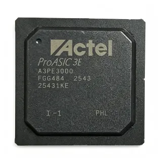
LFE2-20E-6F484I - 21K LUT FPGA, 331 I/O | Lattice Semiconductor
MPN: LFE2-20E-6F484I ✓ فعالLFE2-20E-6F484I جائزہ
An FPGA is a programmable semiconductor in the broader category of programmable logic devices and digital semiconductors. Unlike a fixed-function application-specific integrated circuit, an FPGA implements digital logic through configurable lookup tables, routing resources, registers, block RAM, and programmable I/O. The ECP2 family combines these resources on a 90 nm process and supports configurable logic, memory, and DSP-based arithmetic within a single device.
Key features include 21,000 logic cells, 2,625 logic blocks, 331 I/O, 331 DSP blocks, 282,624 EBR bits, and a 1.2 V operating supply. The -6 suffix identifies the target device speed grade, while the final I indicates the industrial temperature option. Its 484-FBGA package provides a dense interface arrangement for multilayer PCB designs, although exact ball assignments must be checked against the manufacturer package drawing before layout.
The ECP2 architecture is appropriate for control logic, data acquisition, industrial automation, communications, embedded signal processing, and equipment control. Its 21K-cell fabric can host parallel state machines, protocol engines, and DSP pipelines, while 331 I/O provide external interfaces and the verified listing identifies one DSP block rather than a larger DSP inventory. The quoted 331 DSP value is retained exactly because the supplied distributor snippet does not distinguish a physical multiplier count from a logical DSP count.
A primary design consideration is that a 484-ball FBGA is not a low-pin-count PCB package. Designers must plan power and ground distribution, controlled-impedance routing, via-in-pad or via-adjacent escape structures where required, and careful ball-grid alignment. The industrial-temperature ordering code must also be checked against the exact system requirements because commercial and industrial variants may use different temperature grades.
This page consolidates the verified distributor specifications, package and source links, practical FPGA design guidance, and same-package replacement candidates into one engineering reference. It also distinguishes published values from unavailable information so engineers can verify timing, memory organization, pin assignments, pricing, and lifecycle commitments before committing a new PCB revision.
کے لیے ڈراپ اِن متبادل LFE2-20E-6F484I — یکساں پیکیج، پن سے پن مطابقت پذیر۔ مختلف پیکیج والے پرزے جن کے لیے PCB دوبارہ کام درکار ہو، شامل نہیں ہیں۔
اس سیریز میں مختلف ورژن
اسی سیریز کے ماڈلز جو ڈراپ اِن مطابقت رکھتے ہیں LFE2-20E-6F484I (یکساں فارم فیکٹر اور فٹ پرنٹ) — میں مختلف Device Type, Process Technology, Speed Grade, Logic Cells, Package Type.
LFE2-20E-6FN484I
✅ ڈراپ-اِن📋 حوالہ جاتی متبادل (کیٹلاگ میں نہیں)
LFE2-20E-5F484I
✅ ڈراپ-اِنقیمت کے لیے رابطہ کریں
ڈیٹا شیٹ دیکھیں →LFE2-20E-5FN484C
✅ ڈراپ-اِن📋 حوالہ جاتی متبادل (کیٹلاگ میں نہیں)
LFE2-20SE-5FN484C
✅ ڈراپ-اِن📋 حوالہ جاتی متبادل (کیٹلاگ میں نہیں)
LFE2-20SE-6F484I
✅ ڈراپ-اِن📋 حوالہ جاتی متبادل (کیٹلاگ میں نہیں)
LFE2-20E-6F484I زیادہ سے زیادہ ریٹنگز اور برقی خصوصیات
| Device Type | ECP2 Field Programmable Gate Array (FPGA) |
| Logic Cells | 21,000 cells |
| Logic Blocks | 2,625 LABs |
| Lookup Tables | 21K LUTs |
| User I/O | 331 I/O |
| DSP Blocks | 331 DSP |
| Embedded Memory | 282,624 bits |
| سپلائی وولٹیج | 1.2 V |
| Speed Grade | -6 |
| Temperature Grade | Industrial |
| پیکیج | 484-FBGA |
| Number of Terminals | 484 balls |
| Terminal Form | Ball |
| Package Shape | Square |
| Process Technology | 90 nm |
| RoHS اسٹیٹس | Compliant |
LFE2-20E-6F484I square پن کنفیگریشن گائیڈ
LFE2-20E-6F484I (square پیکیج) کے لیے پن کنفیگریشن۔ اس ڈیجیٹل IC میں GPIO، کمیونیکیشن انٹرفیس (UART، SPI، I2C) اور پاور پنز شامل ہیں۔ متبادل پن فنکشنز اور کنفیگریشن آپشنز کے لیے مینوفیکچرر کے ڈیٹا شیٹ سے رجوع کریں۔ ایمبیڈڈ سسٹم ڈیزائن اور PCB لے آؤٹ کے لیے ضروری۔

کے لیے تفصیلی پن آؤٹ ڈیٹا دستیاب نہیں LFE2-20E-6F484I.
رجوع کریں ڈیٹا شیٹ مکمل پن کنفیگریشن کے لیے۔
عام استعمالات
LFE2-20E-6F484I کے لیے موزوں ہے 6 ایپلیکیشنs: Industrial Automation Controller, Industrial Data Acquisition System, Communications Protocol Bridge, Embedded Signal Processing, Programmable Logic Test System, Embedded Network Security Gateway.
Industrial Automation Controller
The LFE2-20E-6F484I fits industrial automation because its 21,000 logic cells can implement sequencing, interlocks, motion-command logic, and communications in one programmable device. The verified ECP2 specification includes 2,625 logic blocks, 331 I/O, and 282,624 EBR bits, providing enough parallel resources for sensor conditioning logic, control tables, and diagnostic state machines. Its 484-FBGA package also supports dense connections to external sensors, power stages, and network transceivers. The -6 speed grade can help timing closure in pipelined control paths, although system timing must be checked against industrial temperature, supply tolerance, and the vendor timing model. Configuration retention, watchdog behavior, and safe-state requirements should also be included in the machine-safety review.
تجویز کردہ
Industrial Data Acquisition System
The LFE2-20E-6F484I is suitable for parallel data acquisition because the ECP2 fabric combines 21,000 logic cells with 282,624 EBR bits and 331 I/O. That resource mix supports sampling control, digital filtering, timestamp handling, packet assembly, and host-interface logic without requiring multiple programmable devices. The -6 grade offers a timing-oriented selection within the family, while 331 I/O provide substantial connectivity for multiplexed sensors and converters. A practical design would partition the fabric into acquisition, processing, and communication regions and constrain interfaces to preserve predictable timing. The verified sources do not provide lane rates, input voltage thresholds, or acquisition accuracy, so those requirements must be checked against the ECP2 and external-converter documentation before selecting voltage thresholds or clocking schemes.
تجویز کردہ
Communications Protocol Bridge
The LFE2-20E-6F484I can implement a multi-interface communications bridge because 21,000 logic cells and 282,624 EBR bits provide room for frame parsing, buffering, state machines, and clock-domain crossing. Its 331 I/O support parallel attachment to Ethernet, serial, and industrial fieldbus transceivers. The ECP2 architecture also permits protocol-specific logic and packet memory to share one device, reducing board count in gateways and embedded controllers. Engineers should use the -6 grade when an existing design has limited timing margin and should verify fabric clock limits and transceiver interface standards for each supported protocol. The supplied distributor data does not list individual transceiver standards, maximum line rate, or security features, so those claims require confirmation from the manufacturer family datasheet and selected companion-device specifications.
تجویز کردہ
Embedded Signal Processing
The LFE2-20E-6F484I can support parallel signal-processing functions when a design needs programmable filters, correlation, interpolation, or fixed-point arithmetic alongside control logic. Its published 21K LUT fabric and 282,624 EBR bits provide configurable computation and buffering, while the -6 performance option can assist clocked pipeline design. The distributor record reports 331 DSP, but the supplied evidence does not clarify whether this is a physical or logical block count; therefore, DSP capacity must be confirmed in the ECP2 family documentation before estimating throughput. A practical implementation would map each filter stage to registered logic, use EBR blocks for line buffers, and keep external memory interfaces limited to the required word width. Final sign-off should include timing analysis at the target voltage and industrial temperature rather than relying only on the ordering-code speed designation.
تجویز کردہ
Programmable Logic Test System
The LFE2-20E-6F484I fits a programmable test or measurement system requiring extensive digital I/O, pattern generation, timing control, and capture memory. Its 331 I/O provide connectivity for device-under-test fixtures, while 21,000 logic cells and 282,624 EBR bits support parallel test vectors, sequencing, and result storage. The -6 grade may provide useful timing margin in systems with demanding clock distribution or synchronized output banks. Designers should partition I/O into matched groups, constrain clocking and output timing, and verify electrical limits for every fixture signal using the ECP2 I/O documentation. The supplied records do not state differential I/O capabilities, maximum user clock frequencies, or output-drive values, so those parameters remain datasheet-selection items rather than assumed design limits.
تجویز کردہ
Embedded Network Security Gateway
The LFE2-20E-6F484I can serve as the programmable core of an embedded gateway that combines packet handling, protocol conversion, local buffering, and supervisory control. The ECP2 device provides 21,000 logic cells, 282,624 EBR bits, and 331 I/O, which can accommodate parallel Ethernet and serial-interface pipelines while reserving logic for boot, health monitoring, and watchdog behavior. The -6 speed grade may help close timing on packet-processing paths. Secure boot, cryptographic acceleration, and memory encryption should not be assumed from the supplied data; those capabilities require verification in the ECP2 security documentation. For production security designs, engineers must also review the device's configuration-read protection mechanisms and lifecycle guarantees. The 484-FBGA package demands careful layer transitions and power distribution, making early signal-integrity and thermal planning essential.
تجویز کردہ
تجویز کردہ پروڈکٹس کا خلاصہ
کے لیے انجینئرنگ ریفرنس ڈیٹا LFE2-20E-6F484I — موازنہ، ڈیزائن رہنمائی، اور تعمیل کی معلومات۔
انتخاب کی گائیڈ
متبادلات کے ساتھ موازنہ
| پیرامیٹر | یہ پروڈکٹ | LFE2-20E-6FN484I | LFE2-20E-5F484I | LFE2-20E-5FN484C | LFE2-20SE-5FN484C | LFE2-20SE-6F484I |
|---|---|---|---|---|---|---|
| Package | 484-FBGA | 484-FBGA - same | 484-FBGA - same | 484-FBGA - same | 484-FBGA - same | 484-FBGA - same |
| Brand | Lattice Semiconductor | Lattice Semiconductor | Lattice Semiconductor | Lattice Semiconductor | Lattice Semiconductor | Lattice Semiconductor |
| Speed Grade | -6 | -6 | -5 | -5 | -5 | -6 |
اہم امتیازی خصوصیات
- Directly documented same-package replacement with matching headline ratings (بمقابلہLFE2-20E-6FN484I)
- Higher performance grade than lower-speed sourcing alternatives (بمقابلہLFE2-20E-5F484I)
- Same 20K-cell ECP2 resource class with a full 331-I/O listing (بمقابلہLFE2-20SE-5FN484C)
ڈیزائن نوٹس
Do not generate the 484-FBGA land pattern from the package name alone. Download the manufacturer drawing for the exact LFE2-20E-6F484I ordering code and verify every ball number, power ball, ground ball, configuration pin, and reserved location. The verified distributor records identify the target as a 484-ball square FBGA, but they do not reproduce the complete ball map. A one-ball or ball-pitch error can create shorts or prevent reliable configuration even when the board outline appears correct.
Plan the core 1.2 V rail as a dedicated power-management branch rather than deriving it directly from an unsynchronized system rail. The supplied records verify a 1.2 V core supply but do not specify tolerance, transient response, or decoupling values. Those figures must be taken from the ECP2 datasheet, and the reference design should be followed for power-grid geometry, bulk capacitance, local ceramic decoupling, and sequencing. Check startup current and configuration behavior before choosing regulators.
The -6 speed designation does not determine a safe board-level trace rate by itself. Establish target interfaces and clock topology during schematic capture, then use the ECP2 timing and I/O documents for input thresholds, output slew, drive strength, and package effects. Maintain continuous return paths beneath high-speed routes, avoid stubs, and route sensitive configuration or clock signals away from switching nodes. Because the supplied data does not state individual I/O standards, these values must not be guessed.
Thermal design should begin with an estimated core-power budget derived from the final logic utilization, clock rates, I/O activity, and selected ECP2 speed grade. The supplied data does not provide thermal resistance or power coefficients, so neither can be estimated responsibly here. After obtaining those values from the manufacturer documentation, compare estimated junction temperature against the industrial-temperature requirement and use split power planes, via arrays, and enclosure airflow as appropriate. Validation should include worst-case ambient temperature and voltage conditions.
تعمیل کی معلومات
RoHS compliance is reported for the closely identified LFE2-20E-6FN484I family member in the supplied search data. The target-specific RoHS statement and all other compliance fields require confirmation against the exact manufacturer product documentation.