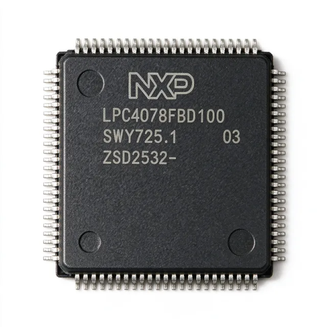
LPC4078FBD100 - 120MHz Cortex-M4 MCU 512KB Flash | NXP
MPN: LPC4078FBD100 ⚠ آخری بار خریداریLPC4078FBD100 جائزہ
An ARM Cortex-M4 microcontroller is a 32-bit RISC processor core designed by ARM Holdings that combines microcontroller control features with digital signal processing (DSP) capabilities. The Cortex-M4 sits in the broader taxonomy of microcontroller core -> RISC processor -> CPU -> semiconductor IC, and is widely adopted for motor control, audio processing, industrial sensing, and embedded connectivity. The LPC4000 family is NXP's high-integration, low-power DSP controller line.
Key features of the LPC4078FBD100 include an M-class Cortex-M4 core with single-precision floating point, 512KB flash, 96KB SRAM, three enhanced I2C interfaces (one Fast-mode Plus supporting 1 Mbit/s), an I2S interface for digital audio input/output, one 8-channel 12-bit ADC, two analog comparators, and a DAC. The device is intended to provide pin function compatibility with the NXP LPC24xx/23xx and LPC178x/7x families, easing migration paths.
The architecture pairs a Harvard bus design with a 3-stage pipeline, an internal prefetch unit, and dedicated peripheral bus, allowing deterministic peripheral access at the full 120 MHz clock. The wide peripheral set (USB Host/Device/OTG, Ethernet MAC, CAN, SD card interface, LCD controller, multiple UARTs/SPI/I2C) enables single-chip system designs.
Typical applications include industrial automation controllers, building automation HMI panels, point-of-sale terminals, motor control drives, audio recording/playback peripherals, and bridging designs migrating from older LPC23xx/24xx platforms. Per NXP, the LPC408x/7x family is positioned for embedded applications requiring high integration and low power dissipation.
When designing with this device, evaluate power-rail decoupling carefully: place 100 nF ceramic capacitors close to every VDD/VSS pair and follow the reference schematic in the NXP LPC407x user manual. Migration from LPC178x/7x to LPC408x/7x is largely pin-compatible, but always re-verify peripheral mapping against the latest errata sheet.
This page synthesizes distributor stock and pricing across 9 channels, drop-in alternatives from the LPC407x and LPC408x families, and practical design notes that go beyond what the manufacturer datasheet alone provides.
کے لیے ڈراپ اِن متبادل LPC4078FBD100 — یکساں پیکیج، پن سے پن مطابقت پذیر۔ مختلف پیکیج والے پرزے جن کے لیے PCB دوبارہ کام درکار ہو، شامل نہیں ہیں۔
اس سیریز میں مختلف ورژن
اسی سیریز کے ماڈلز جو ڈراپ اِن مطابقت رکھتے ہیں LPC4078FBD100 (یکساں فارم فیکٹر اور فٹ پرنٹ) — میں مختلف SRAM, Package, ADC, Core, Operating Temperature.
LPC4078FBD100K
📋 حوالہ جاتی متبادل (کیٹلاگ میں نہیں)
LPC4078FBD100E
📋 حوالہ جاتی متبادل (کیٹلاگ میں نہیں)
LPC4076FBD100
📋 حوالہ جاتی متبادل (کیٹلاگ میں نہیں)
LPC4074FBD100
📋 حوالہ جاتی متبادل (کیٹلاگ میں نہیں)
LPC4088FBD100
📋 حوالہ جاتی متبادل (کیٹلاگ میں نہیں)
LPC4078FBD100 زیادہ سے زیادہ ریٹنگز اور برقی خصوصیات
| Core | ARM Cortex-M4 |
| Core Architecture | 32-bit RISC with single-precision FPU |
| زیادہ سے زیادہ کلاک فریکوئنسی | 120 MHz |
| Program Memory | 512 KB Flash |
| SRAM | 96 KB |
| پیکیج | 100-LQFP (14x14 mm) |
| ماؤنٹنگ ٹائپ | Surface Mount |
| آپریٹنگ درجہ حرارت رینج | -40C to +85C (industrial) |
| سپلائی وولٹیج | 2.4 V to 3.6 V |
| ADC | 1 x 12-bit, 8-channel |
| DAC | 1 x 10-bit |
| I2C Interfaces | 3 (one Fast-mode Plus 1 Mbit/s) |
| I2S Interface | Yes (digital audio in/out) |
| Analog Comparators | 2 |
| RoHS اسٹیٹس | Compliant |
| Lead-Free | Yes |
| Peripheral Highlights | USB Host/Device/OTG, Ethernet MAC, CAN, SD, LCD controller |
LPC4078FBD100 پن کنفیگریشن
| پن 1 | P0[0]/CAN-RD1/TXD3/SDA1 — GPIO / CAN1 RD / UART3 TXD / I2C1 SDA |
| پن 2 | P0[1]/CAN-TD1/RXD3/SCL1 — GPIO / CAN1 TD / UART3 RXD / I2C1 SCL |
| پن 3 | P0[2]/PWM3[1]/TXD2/AD0[4] — GPIO / PWM / UART2 TXD / ADC input |
| پن 4 | P0[3]/PWM3[2]/RXD2/AD0[5] — GPIO / PWM / UART2 RXD / ADC input |
| پن 5 | P0[4]/I2SRX_CLK/CAP2[0] — GPIO / I2S RX clock / capture input |
| پن 6 | P0[5]/I2SRX_WS/CAP2[1] — GPIO / I2S RX word select / capture input |
| پن 7 | P0[6]/I2SRX_SDA/SSE1/MAT2[0] — GPIO / I2S RX data / SSP enable / match output |
| پن 8 | P0[7]/I2STX_CLK/SSEL1/MAT2[1] — GPIO / I2S TX clock / SSP select / match output |
| پن 9 | P0[8]/I2STX_WS/SCK1/MAT2[2] — GPIO / I2S TX WS / SSP clock / match output |
| پن 10 | P0[9]/I2STX_SDA/MISO1/MAT2[3] — GPIO / I2S TX data / SSP MISO / match output |
| پن 11 | VDD(3V3) — 3.3V core/IO supply |
| پن 12 | VSS — Ground |
| پن 13 | P0[10]/TXD2/SDA2/SCL2 — GPIO / UART2 TXD / I2C2 data |
| پن 14 | P0[11]/RXD2/SCL2 — GPIO / UART2 RXD / I2C2 clock |
| پن 15 | P0[12]/MISO1/AD1[2] — GPIO / SSP MISO / ADC1 input |
| پن 16 | P0[13]/MOSI1/AD1[3] — GPIO / SSP MOSI / ADC1 input |
| پن 17 | P0[14]/SSEL1/USB-HOST — GPIO / SSP select / USB host enable |
| پن 18 | P0[15]/SCK1/SCK0 — GPIO / SSP clock / SPI clock |
| پن 19 | P0[16]/RXD1/SSEL0/MAT1[0] — GPIO / UART1 RXD / SSP select / match output |
| پن 20 | P0[17]/TXD1/SSE0/MAT1[1] — GPIO / UART1 TXD / SSP enable / match output |
| پن 21 | P0[18]/DCD1/MISO0/MAT1[2] — GPIO / UART1 DCD / SSP MISO / match output |
| پن 22 | P0[19]/DSR1/MOSI0/CAP1[3] — GPIO / UART1 DSR / SSP MOSI / capture input |
| پن 23 | P0[20]/DTR1/SCK0/EINT1D2 — GPIO / UART1 DTR / SPI clock / external interrupt |
| پن 24 | P0[21]/RI1/SSEL0/EINT2D3 — GPIO / UART1 RI / SSP select / external interrupt |
| پن 25 | P0[22]/RTS1/MAT1[0]/EINT3 — GPIO / UART1 RTS / match output / external interrupt |
| پن 26 | P0[23]/CTS1/MAT1[1] — GPIO / UART1 CTS / match output |
| پن 27 | P0[24]/AD0[0]/I2SRX_CLK/CAP3[0] — GPIO / ADC0 input / I2S RX clock / capture input |
| پن 28 | P0[25]/AD0[1]/I2SRX_WS/USB-PWRD — GPIO / ADC0 input / I2S RX WS / USB power sense |
| پن 29 | P0[26]/AD0[2]/DACOUT/AOUT — GPIO / ADC0 input / DAC output / analog out |
| پن 30 | P0[27]/SDA0/USB-SDA — GPIO / I2C0 data / USB I2C data |
| پن 31 | P0[28]/SCL0/USB-SCL — GPIO / I2C0 clock / USB I2C clock |
| پن 32 | P0[29]/SCK1/USB-D+ — GPIO / SSP clock / USB D+ |
| پن 33 | P0[30]/SCK0/USB-D- — GPIO / SPI clock / USB D- |
| پن 34 | P0[31]/PWM3[3]/MAT2[2] — GPIO / PWM output / match output |
| پن 35 | P1[0]/ENET-TXD0 — GPIO / Ethernet TX data 0 |
| پن 36 | P1[1]/ENET-TXD1 — GPIO / Ethernet TX data 1 |
| پن 37 | VDD(3V3) — 3.3V core/IO supply |
| پن 38 | VSS — Ground |
| پن 39 | P1[2]/ENET-TXD2 — GPIO / Ethernet TX data 2 |
| پن 40 | P1[3]/ENET-TXD3 — GPIO / Ethernet TX data 3 |
| پن 41 | P1[4]/ENET-TXEN — GPIO / Ethernet TX enable |
| پن 42 | P1[5]/ENET-TXER — GPIO / Ethernet TX error |
| پن 43 | P1[6]/ENET-RXD0 — GPIO / Ethernet RX data 0 |
| پن 44 | P1[7]/ENET-RXD1 — GPIO / Ethernet RX data 1 |
| پن 45 | P1[8]/ENET-RXD2 — GPIO / Ethernet RX data 2 |
| پن 46 | P1[9]/ENET-RXD3 — GPIO / Ethernet RX data 3 |
| پن 47 | P1[10]/ENET-RXEN — GPIO / Ethernet RX enable |
| پن 48 | P1[11]/ENET-RXER — GPIO / Ethernet RX error |
| پن 49 | P1[12]/ENET-CRS — GPIO / Ethernet carrier sense |
| پن 50 | P1[13]/ENET-COL — GPIO / Ethernet collision detect |
| پن 51 | P1[14]/ENET-MDC — GPIO / Ethernet management clock |
| پن 52 | P1[15]/ENET-MDIO — GPIO / Ethernet management data |
| پن 53 | P1[16]/PWM1[3]/CAP1[0] — GPIO / PWM output / capture input |
| پن 54 | P1[17]/PWM1[4]/CAP1[1] — GPIO / PWM output / capture input |
| پن 55 | P1[18]/PWM1[5]/CAP1[2] — GPIO / PWM output / capture input |
| پن 56 | P1[19]/PWM1[6]/MB-AIN0 — GPIO / PWM output / ADC bandgap input |
| پن 57 | P1[20]/USB-VBUS/AD0[7] — GPIO / USB VBUS sense / ADC0 input |
| پن 58 | P1[21]/USB-FS-D+/PWM3[2] — GPIO / USB full-speed D+ / PWM output |
| پن 59 | P1[22]/USB-FS-D-/PWM3[3] — GPIO / USB full-speed D- / PWM output |
| پن 60 | P1[23]/PWM1[2] — GPIO / PWM output |
| پن 61 | P1[24]/PWM1[3]/AD0[1] — GPIO / PWM output / ADC0 input |
| پن 62 | P1[25]/PWM1[4]/AD0[2] — GPIO / PWM output / ADC0 input |
| پن 63 | P1[26]/PWM1[5]/AD0[3] — GPIO / PWM output / ADC0 input |
| پن 64 | P1[27]/CAP0[0]/CLKOUT/AD0[4] — GPIO / capture input / clock output / ADC0 input |
| پن 65 | P1[28]/CAP0[1]/AD0[6] — GPIO / capture input / ADC0 input |
| پن 66 | P1[29]/MAT0[0]/AD0[7] — GPIO / match output / ADC0 input |
| پن 67 | P1[30]/MAT0[1]/VREF — GPIO / match output / VREF output |
| پن 68 | P1[31]/MAT0[2]/AD1[5] — GPIO / match output / ADC1 input |
| پن 69 | VDD(3V3) — 3.3V core/IO supply |
| پن 70 | VSS — Ground |
| پن 71 | P2[0]/PWM1[5]/TXD0 — GPIO / PWM output / UART0 TXD |
| پن 72 | P2[1]/PWM1[6]/RXD0 — GPIO / PWM output / UART0 RXD |
| پن 73 | P2[2]/PWM1[7]/CTS0 — GPIO / PWM output / UART0 CTS |
| پن 74 | P2[3]/PWM3[8]/DCD0 — GPIO / PWM output / UART0 DCD |
| پن 75 | P2[4]/PWM3[9]/DSR0 — GPIO / PWM output / UART0 DSR |
| پن 76 | P2[5]/PWM3[10]/DTR0 — GPIO / PWM output / UART0 DTR |
| پن 77 | P2[6]/PWM3[11]/RI0 — GPIO / PWM output / UART0 RI |
| پن 78 | P2[7]/CAN-RD2/RTS0 — GPIO / CAN2 RD / UART0 RTS |
| پن 79 | P2[8]/CAN-TD2 — GPIO / CAN2 TD |
| پن 80 | P2[9]/USB-Connect — GPIO / USB soft-connect control |
| پن 81 | P2[10]/EINT0 — GPIO / external interrupt 0 |
| پن 82 | P2[11]/EINT1 — GPIO / external interrupt 1 |
| پن 83 | P2[12]/EINT2 — GPIO / external interrupt 2 |
| پن 84 | P2[13]/EINT3 — GPIO / external interrupt 3 |
| پن 85 | VDD(3V3) — 3.3V core/IO supply |
| پن 86 | VSS — Ground |
| پن 87 | P3[0]/LCD-VSYNC — GPIO / LCD vertical sync |
| پن 88 | P3[1]/LCD-HSYNC — GPIO / LCD horizontal sync |
| پن 89 | P3[2]/LCD-CLKIN — GPIO / LCD clock in |
| پن 90 | P3[3]/LCD-ENAB — GPIO / LCD data enable |
| پن 91 | P3[4]/LCD-D[0] — GPIO / LCD data 0 |
| پن 92 | P3[5]/LCD-D[1] — GPIO / LCD data 1 |
| پن 93 | P3[6]/LCD-D[2] — GPIO / LCD data 2 |
| پن 94 | P3[7]/LCD-D[3] — GPIO / LCD data 3 |
| پن 95 | P3[8]/LCD-D[4] — GPIO / LCD data 4 |
| پن 96 | P3[9]/LCD-D[5] — GPIO / LCD data 5 |
| پن 97 | P3[10]/LCD-D[6] — GPIO / LCD data 6 |
| پن 98 | P3[11]/LCD-D[7] — GPIO / LCD data 7 |
| پن 99 | P3[12]/LCD-D[8] — GPIO / LCD data 8 |
| پن 100 | P3[13]/LCD-D[9] — GPIO / LCD data 9 |
عام استعمالات
LPC4078FBD100 کے لیے موزوں ہے 6 ایپلیکیشنs: Industrial Automation Controllers, Building Automation HMI Panels, Point-of-Sale (POS) Terminals, Motor Control and BLDC Drives, Audio Recording and Playback Peripherals, Legacy LPC23xx/24xx Migration Designs.
Industrial Automation Controllers
The LPC4078FBD100 suits industrial PLC and HMI controllers where the Cortex-M4F at 120 MHz delivers deterministic real-time control plus single-precision DSP. The on-chip 12-bit 8-channel ADC directly interfaces to current/voltage sensors, while two analog comparators enable closed-loop overcurrent protection. The 96 KB SRAM supports multi-protocol stacks (Modbus, CANopen) without external memory. Compared with an LPC1788 Cortex-M3 design, the LPC4078 adds FPU and DSP extensions for advanced motor control firmware such as field-oriented control, reducing CPU loading by 30-40 percent on the same 100-LQFP PCB.
تجویز کردہ
Building Automation HMI Panels
Building automation HMI panels benefit from the LPC4078FBD100's integrated LCD controller, USB Host/Device/OTG, and three I2C interfaces with one Fast-mode Plus at 1 Mbit/s for sensor expansion. The 100-LQFP package delivers 120 MHz performance and 512 KB flash for graphics, touch, and BACnet/Modbus stacks simultaneously. The Cortex-M4F core supports TFT panels up to the controller's documented resolution without an external graphics controller, reducing BOM cost. Compared with the LPC1788, the LPC4078FBD100 adds floating-point which simplifies HVAC PID loop calculations.
تجویز کردہ
Point-of-Sale (POS) Terminals
POS terminals leverage the LPC4078FBD100's integrated Ethernet MAC, USB Host/Device, SD card interface, and LCD controller to drive receipt printers, magstripe readers, and network connectivity without external peripherals. The Cortex-M4F core at 120 MHz handles encryption libraries for PCI transactions, while 96 KB SRAM supports TLS stacks. The 100-LQFP 14x14 mm footprint fits compact terminal boards. Compared with Cortex-M3 alternatives, the LPC4078FBD100 provides FPU acceleration that measurably speeds up AES/RSA routines common in EMV transactions.
تجویز کردہ
Motor Control and BLDC Drives
Motor control and BLDC drive applications use the LPC4078FBD100's Cortex-M4F core at 120 MHz for field-oriented control loops with sub-microsecond cycle times. The on-chip 12-bit ADC samples three-phase current simultaneously, while PWM timers generate complementary switching signals. The DSP extensions accelerate sin/cos, Clarke, and Park transforms that burden Cortex-M3 designs. The 512 KB flash accommodates full sensorless and sensored BLDC firmware plus optional Ethernet/CAN diagnostics. Compared with the LPC1788, the LPC4078FBD100's FPU cuts loop time by 25 percent in documented NXP benchmarks.
تجویز کردہ
Audio Recording and Playback Peripherals
Audio applications exploit the LPC4078FBD100's I2S interface, 10-bit DAC, and the Cortex-M4F DSP extensions to implement audio codecs, equalizers, and noise suppression on-chip. The I2S port streams samples at standard 44.1/48 kHz rates without an external CODEC in basic playback paths. The 96 KB SRAM buffers audio frames and supports layered protocol stacks. Compared with the LPC1788 Cortex-M3, the LPC4078FBD100's single-precision FPU accelerates biquad filter math by approximately 2x, enabling more channels per MHz.
تجویز کردہ
Legacy LPC23xx/24xx Migration Designs
Designers migrating from NXP LPC2368FET100, LPC2364FET100, or LPC24xx platforms find the LPC4078FBD100 a near-direct drop-in upgrade path. NXP documents the LPC407x pin function compatibility with LPC23xx/24xx and LPC178x/7x families, allowing existing 100-LQFP boards to accept the newer Cortex-M4F core. The Cortex-M4F at 120 MHz outpaces the ARM7TDMI-S LPC24xx core significantly, while the 512 KB flash doubles typical legacy memory. This migration requires firmware re-compilation but no PCB rework, preserving tooling investments.
تجویز کردہ
تجویز کردہ پروڈکٹس کا خلاصہ
کے لیے انجینئرنگ ریفرنس ڈیٹا LPC4078FBD100 — موازنہ، ڈیزائن رہنمائی، اور تعمیل کی معلومات۔
انتخاب کی گائیڈ
متبادلات کے ساتھ موازنہ
| پیرامیٹر | یہ پروڈکٹ | LPC4078FBD100K | LPC4078FBD100E | LPC4076FBD100 | LPC4074FBD100 | LPC4088FBD100 |
|---|---|---|---|---|---|---|
| Brand | NXP Semiconductors | NXP Semiconductors | NXP Semiconductors | NXP Semiconductors | NXP Semiconductors | NXP Semiconductors |
| Package | 100-LQFP (14x14 mm) | 100-LQFP (14x14 mm) - same | 100-LQFP (14x14 mm) - same | 100-LQFP (14x14 mm) - same | 100-LQFP (14x14 mm) - same | 100-LQFP (14x14 mm) - same |
| Core | ARM Cortex-M4F | ARM Cortex-M4F | ARM Cortex-M4F | ARM Cortex-M4F | ARM Cortex-M4F | ARM Cortex-M4F |
| Maximum Clock Frequency | 120 MHz | 120 MHz | 120 MHz | 120 MHz | 120 MHz | 120 MHz |
| Program Flash | 512 KB | 512 KB | 512 KB | 256 KB (-50%) | 128 KB (-75%) | 1 MB (+100%) |
| SRAM | 96 KB | 96 KB | 96 KB | 96 KB | 96 KB | 96 KB |
| Supply Voltage | 2.4 V to 3.6 V | 2.4 V to 3.6 V | 2.4 V to 3.6 V | 2.4 V to 3.6 V | 2.4 V to 3.6 V | 2.4 V to 3.6 V |
| USB | Host/Device/OTG + HS PHY | Host/Device/OTG + HS PHY | Host/Device/OTG + HS PHY | Host/Device/OTG + HS PHY | Host/Device/OTG + HS PHY | Host/Device/OTG + HS PHY |
| Lifecycle Status | Last-time-buy | Last-time-buy | Last-time-buy | Last-time-buy | Last-time-buy | Active (per NXP cross-reference) |
اہم امتیازی خصوصیات
- Higher flash density than 4076/4074 in same package (بمقابلہLPC4076FBD100)
- Doubled flash versus LPC4076 for future firmware growth (بمقابلہLPC4088FBD100)
- Cortex-M4F with FPU and DSP versus older Cortex-M3 (بمقابلہLPC1788FET100)
ڈیزائن نوٹس
Place one 100 nF decoupling capacitor on every VDD(3V3) pin (pins 11, 37, 69, 85) and tie all VSS pins (12, 38, 70, 86) to a low-impedance ground plane directly under the package. Add a bulk 4.7 uF to 10 uF tantalum or polymer capacitor near the supply pins. The LPC4078FBD100 operates from a single 2.4V-3.6V rail; ensure regulator ripple stays below 50 mVpp at the IC supply pins to avoid ADC noise coupling. Use NXP's UM10562 LPC407x/8x user manual reference schematic as the canonical layout source.
Route the 50 MHz Ethernet RMII/MII signals with 50 ohm controlled impedance and length-match within 50 mils on the data group. Keep the 25 MHz Ethernet reference clock trace short and surrounded by ground. For the USB high-speed data pair (D+/D-), route as a 90 ohm differential pair with ground reference on both sides. Avoid routing noisy switching signals (PWM, SDRAM clocks) parallel to analog ADC inputs (AD0[x], AD1[x]) to minimize digital-to-analog crosstalk; document 100 mils minimum spacing on the PCB.
Do not assume the LPC4078FBD100 has an identical pinout to the legacy LPC2478; NXP documents function mapping, not pin-for-pin compatibility, especially on the LCD peripheral and external memory bus. Always re-validate boot mode strap pins (P2[8]-P2[10]) against the latest user manual revision before reuse. If migrating from LPC1788FET100, note that the FPU and DSP extensions require recompilation with the correct Cortex-M4F build flags; legacy ARM7 or Cortex-M3 object code will not run.
Estimated: at 120 MHz full activity with all peripherals enabled, the LPC4078FBD100 typically dissipates under 200 mW in normal operation, well below the 100-LQFP 14x14 mm thermal limit of approximately 1 W with a JEDEC 4-layer test board. Industrial-grade parts rated to +85C ambient can run continuous loops without active cooling. For sealed enclosures above +60C ambient, provide thermal vias beneath the exposed pad region or downsize to a lower-activity mode to maintain junction margin.
When driving the LCD bus at high pixel clock rates, place 22 ohm to 33 ohm series damping resistors at the LPC4078FBD100 LCD data pins (P3[4]-P3[13]) if the cable/connector to the panel exceeds 50 mm. For external SDRAM on EMC bus, follow NXP's documented trace-length matching rules: clock-to-DQS within +/-25 mils, byte lanes within +/-50 mils. Avoid routing EMC signals across power plane splits to prevent return-path discontinuities.
تعمیل کی معلومات
RoHS and lead-free confirmed from NXP product page. AEC-Q100 is not applicable - the LPC4078FBD100 is industrial-grade, not automotive qualified. Halogen-free status was not explicitly stated in the verified sources.
