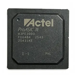
M2GL050T-FG484 - 56340-Cell 1.2V Flash FPGA | Microchip
MPN: M2GL050T-FG484 ✗ اختتامِ زندگیM2GL050T-FG484 جائزہ
An FPGA is a programmable semiconductor whose logic, routing, and I/O resources can be configured after manufacture. The M2GL050 belongs to the IGLOO2 hierarchy of flash FPGAs, a device family positioned between simple programmable logic and larger programmable SoC products. Its flash configuration architecture retains the programmed design in non-volatile memory, allowing the circuit to begin operation without loading a separate configuration file into volatile memory at every power cycle.
The principal device characteristics include 56,340 logic cells, 267 available I/O in the referenced ordering information, and a 1.2 V operating core voltage. These resources support interfaces, control logic, protocol bridges, and data-format conversion while retaining the operational flexibility associated with reprogrammable hardware. The 484-FBGA package provides a high pin count for systems requiring extensive parallel connectivity.
As an IGLOO2 device, the M2GL050T-FG484 supports general-purpose programmable functions across communications, industrial, medical, defense, and aviation systems. Its non-volatile configuration is especially useful where rapid startup, deterministic system availability, or field reconfiguration is more important than the flexibility of a soft microcontroller core. The high-I/O package also makes the device relevant to complex board-level interconnect and signal-conversion designs.
Typical applications include general-purpose bridging functions, input/output expansion, data-format conversion, system management, secure connectivity, and control-plane logic. The same device family is also used in communications equipment, industrial controllers, medical systems, and defense or aviation platforms where programmable post-deployment updates and compact logic integration are valuable.
The principal design consideration is package and I/O verification. Because the device uses a 484-ball FBGA with 267 listed I/O, the board layout must follow the manufacturer's ball map, power, configuration, and decoupling guidance. A design should also confirm that its clocking, supported I/O standards, voltage requirements, and programming method satisfy the selected IGLOO2 device before schematic or PCB release.
This page consolidates device-family positioning, verified ordering information, practical application guidance, drop-in alternatives, and engineering-focused comparisons. It helps designers separate logic-capacity, package, speed-grade, and temperature-grade differences before committing a 484-ball programmable-logic design to production.
کے لیے ڈراپ اِن متبادل M2GL050T-FG484 — یکساں پیکیج، پن سے پن مطابقت پذیر۔ مختلف پیکیج والے پرزے جن کے لیے PCB دوبارہ کام درکار ہو، شامل نہیں ہیں۔
اس سیریز میں مختلف ورژن
اسی سیریز کے ماڈلز جو ڈراپ اِن مطابقت رکھتے ہیں M2GL050T-FG484 (یکساں فارم فیکٹر اور فٹ پرنٹ).
M2GL050T-1FG484M
✅ ڈراپ-اِن📋 حوالہ جاتی متبادل (کیٹلاگ میں نہیں)
M2GL050T-1FG484
✅ ڈراپ-اِن📋 حوالہ جاتی متبادل (کیٹلاگ میں نہیں)
M2GL050T-FGG484
✅ ڈراپ-اِن📋 حوالہ جاتی متبادل (کیٹلاگ میں نہیں)
M2GL050T-FG484I
✅ ڈراپ-اِن📋 حوالہ جاتی متبادل (کیٹلاگ میں نہیں)
M2GL050T-1FGG484I
✅ ڈراپ-اِن📋 حوالہ جاتی متبادل (کیٹلاگ میں نہیں)
M2GL050T-FG484 زیادہ سے زیادہ ریٹنگز اور برقی خصوصیات
| Product Type | Flash-based field-programmable gate array (FPGA) |
| FPGA Family | IGLOO2 |
| Logic Cells | 56,340 cells |
| User I/O | 267 I/O |
| Core Supply Voltage | 1.2 V |
| Package Type | 484-FBGA |
| Ball Count | 484 balls |
| Package Pitch | 1.0 mm |
| Package Dimension | 2.44 mm |
| Configuration Memory | Embedded non-volatile flash |
| Programmability | User-programmable logic and I/O |
M2GL050T-FG484 2.44 mm پن کنفیگریشن گائیڈ
M2GL050T-FG484 (2.44 mm پیکیج) کے لیے پن کنفیگریشن۔ اس ڈیجیٹل IC میں GPIO، کمیونیکیشن انٹرفیس (UART، SPI، I2C) اور پاور پنز شامل ہیں۔ متبادل پن فنکشنز اور کنفیگریشن آپشنز کے لیے مینوفیکچرر کے ڈیٹا شیٹ سے رجوع کریں۔ ایمبیڈڈ سسٹم ڈیزائن اور PCB لے آؤٹ کے لیے ضروری۔

کے لیے تفصیلی پن آؤٹ ڈیٹا دستیاب نہیں M2GL050T-FG484.
رجوع کریں ڈیٹا شیٹ مکمل پن کنفیگریشن کے لیے۔
عام استعمالات
M2GL050T-FG484 کے لیے موزوں ہے 6 ایپلیکیشنs: General-Purpose Protocol Bridging, Industrial I/O Expansion, Data Format Conversion, Secure Connectivity Control, Medical System Management, Aerospace and Defense Control Logic.
General-Purpose Protocol Bridging
The M2GL050T-FG484 fits protocol-bridging designs that need substantial parallel connectivity and flexible post-deployment logic changes. Its 56,340 logic cells provide capacity for endpoint translation, buffering, arbitration, status translation, and control logic, while 267 I/O supports parallel interfaces across multiple voltage domains. The 1.2 V core operation and embedded flash configuration suit equipment where predictable startup and retained configuration are important. Designers should partition interfaces according to the IGLOO2 banking rules, confirm supported I/O standards for every external device, and validate timing with the same clock conditions used in production. The 484-FBGA package also demands careful escape routing and power-plane planning.
تجویز کردہ
Industrial I/O Expansion
M2GL050T-FG484 is suitable for industrial I/O expansion when a controller must add many discrete inputs, outputs, counters, or interlocks without implementing them as fixed logic. The FPGA's 56,340 logic cells can support state machines, debouncing, diagnostics, data registers, and communication formatting, while its 267 I/O provide a large interface budget. Embedded flash allows the configuration to remain available across power cycles, which supports deterministic recovery after resets. For industrial deployment, verify the exact temperature grade, isolation boundaries, input thresholds, output drive limits, and supported I/O standards. The design should also use the manufacturer's bank and pin-description guide to prevent incompatible voltage combinations or signal-integrity problems.
تجویز کردہ
Data Format Conversion
The M2GL050T-FG484 can implement compact data-format conversion engines by combining parallel I/O with programmable pipelines, lookup logic, and buffering. Its 56,340 logic cells are suitable for transformations such as byte ordering, packing and unpacking, parallel-to-serial formatting, frame synchronization, and status-code generation. The 1.2 V core and flash-based configuration help designers implement low-latency logic close to external interfaces without a separate configuration loader. Clock-domain requirements must be handled with the appropriate IGLOO2 clocking resources, and every high-speed interface should be verified against supported I/O standards. Placement near the associated connector or memory can reduce routing delay, but the 484-ball package still requires disciplined power and return-path planning.
تجویز کردہ
Secure Connectivity Control
The M2GL050T-FG484 fits secure-connectivity control functions that combine link management, key or session logic, status monitoring, and protocol-specific adaptation in one programmable device. Its 56,340 logic cells and 267 I/O provide enough resources to sit between processors and communication PHYs while retaining the ability to update logic in the field. Non-volatile flash configuration supports rapid system availability, although application-level security still requires suitable authentication, key protection, and tamper-control measures. Engineers should partition sensitive and non-sensitive paths, prevent unneeded interfaces from being routed, and validate all external voltage domains against the package pin data. The 1.2 V core supply must also be generated with low-noise, stable power to avoid logic or I/O margin loss.
تجویز کردہ
Medical System Management
M2GL050T-FG484 is applicable to medical and diagnostic equipment that needs flexible supervisory logic, interface conversion, and persistent control behavior. The device can implement alarm sequencing, sensor-path control, status aggregation, and communication adapters using its 56,340 logic cells and 267 I/O. Embedded flash provides retained configuration, but medical designs must still apply the applicable risk analysis, electrical-safety separation, and environmental qualification for the finished system. Verify the exact temperature range and supported I/O standards rather than assuming that the package name defines medical suitability. Keep patient-connected circuitry isolated from programmable logic where required, and validate reset behavior, brownout response, and configuration integrity as part of system-level verification.
تجویز کردہ
Aerospace and Defense Control Logic
M2GL050T-FG484 can support compact control and interface logic in aerospace, defense, and aviation-related equipment where programmable functions and non-volatile configuration are useful. The 56,340-cell device can combine command decoding, redundant status handling, bus adaptation, and embedded monitoring, while 267 I/O provides extensive connectivity for system-level integration. Qualification for a particular airborne program must be confirmed independently through the exact ordering code and applicable Microchip qualification documentation. The 1.2 V core operating point needs a stable supply with appropriate sequencing and monitoring, while the 484-FBGA layout must follow the manufacturer's escape, decoupling, and thermal guidance. Functional equivalence of a replacement should include environmental, lifecycle, and configuration-retention checks.
تجویز کردہ
تجویز کردہ پروڈکٹس کا خلاصہ
کے لیے انجینئرنگ ریفرنس ڈیٹا M2GL050T-FG484 — موازنہ، ڈیزائن رہنمائی، اور تعمیل کی معلومات۔
انتخاب کی گائیڈ
متبادلات کے ساتھ موازنہ
| پیرامیٹر | یہ پروڈکٹ | M2GL050T-1FG484M | M2GL050T-1FG484 | M2GL050T-FGG484 | M2GL050T-FG484I | M2GL050T-1FGG484I |
|---|---|---|---|---|---|---|
| Brand | Microchip Technology | Microchip Technology | Microchip Technology | Microchip Technology | Microchip Technology | Microchip Technology |
| Package | 484-FBGA | 484-FBGA | 484-FBGA | 484-FBGA | 484-FBGA | 484-FBGA |
| FPGA Family | IGLOO2 | IGLOO2 | IGLOO2 | IGLOO2 | IGLOO2 | IGLOO2 |
| Logic Cells | 56,340 cells | 56,340 cells | 56,340 cells | 56,340 cells | 56,340 cells | 56,340 cells |
| User I/O | 267 I/O | 267 I/O | 267 I/O | 267 I/O | 267 I/O | 267 I/O |
| Core Supply Voltage | 1.2 V | 1.2 V | 1.2 V | 1.2 V | 1.2 V | 1.2 V |
| Configuration Memory | Embedded non-volatile flash | Embedded non-volatile flash | Embedded non-volatile flash | Embedded non-volatile flash | Embedded non-volatile flash | Embedded non-volatile flash |
| Speed-Grade Ordering Difference | Base M2GL050T-FG484 ordering code | -1 speed designation | -1 speed designation | FGG speed designation | No -1 speed designation | -1 speed designation |
| Temperature-Grade Ordering Difference | No trailing I in target ordering code | No trailing I | No trailing I | No trailing I | Trailing I | Trailing I |
اہم امتیازی خصوصیات
- Original ordering-code match for existing 484-ball designs (بمقابلہM2GL050T-FGG484)
- Exact target identity without an industrial temperature suffix (بمقابلہM2GL050T-FG484I)
- High logic and I/O density in the original device specification (بمقابلہM2GL050T-1FG484M)
ڈیزائن نوٹس
Treat the 484-FBGA land pattern as a high-density routing problem. Follow Microchip's IGLOO2 packaging and pin-description guide for ball locations, power pins, configuration pins, and I/O banks; do not derive assignments from a generic 484-BGA drawing. Keep continuous return paths beneath the device, minimize loop area around power and configuration balls, and route clocks away from high-slew-rate outputs. Because the package uses a 1.0 mm pitch, assembly capability, solder mask definition, and paste-volume control should be reviewed with the PCB fabricator before release.
The M2GL050T-FG484 operates from a 1.2 V core supply, so power delivery must account for the core, configuration activity, and the external loads driven by its 267 I/O. Confirm permitted voltage combinations, static and dynamic current limits, supply sequencing, and I/O drive settings from the family documentation before finalizing the regulator. Place local decoupling at the relevant supply balls using the manufacturer-recommended network, and verify power-up behavior across maximum load, temperature, and configuration states. Do not infer the 1.2 V core value as the permitted voltage for every user I/O.
Do not approve a replacement solely because its part number ends in 484. The M2GL050T-1FG484, M2GL050T-FGG484, and I-suffixed variants can change speed or temperature ordering options. For every candidate, compare the complete Microchip ordering table, timing limits, operating-temperature range, configuration interface, and lifecycle state. After substitution, recompile the design, rerun static timing at the production clock, and inspect any new I/O or power warnings. The -1 variants are identified as not recommended for new designs, with M2GL060 named as the recommended successor.
Assign the 267 I/O to clock and data paths according to bank and clock-resource capabilities rather than using pin numbers alone. Keep sensitive or high-speed interfaces away from noisy power-conversion regions, and match trace lengths where source-synchronous timing depends on skew control. For externally clocked interfaces, validate source termination, I/O standard, drive strength, slew rate, and input threshold in the device configuration. PCB signal-integrity simulation should be performed for the highest-rate interfaces because package and board effects can consume timing margin that is not visible in resource-only comparisons.
تعمیل کی معلومات
The retrieved product and distributor information does not explicitly state the compliance status for the exact M2GL050T-FG484 ordering code. Review the Microchip product documentation and current declarations before production release.