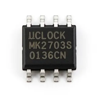
MK2304S-1ILF - 133MHz Zero-Delay Buffer | Renesas
MPN: MK2304S-1ILF ✓ فعالMK2304S-1ILF جائزہ
A zero-delay buffer is a clock-management device that reproduces an input clock at an output with very little added delay. It sits between a clock source and a load when the system needs a clean, repeatable clock distribution point rather than the longer and less deterministic delay of ordinary buffered wiring. In the broader semiconductor hierarchy, this device is a clock buffer, a type of clock and timing IC, and a member of the wider semiconductor and digital signal-conditioning product categories.
The primary identified specifications are a maximum operating frequency of 133 MHz, one buffered output channel, and an 8-SOIC package measuring approximately 3.90 mm in width. The MK2304S-1ILF is identified as a low-skew zero-delay design, making it appropriate for systems that distribute a periodic reference clock to multiple logic or communications circuits. The -1ILF ordering code identifies the specific manufacturer configuration rather than a generic clock-buffer function.
Unlike a crystal oscillator, the MK2304S-1ILF does not create a frequency; it preserves and redistributes an externally generated clock. Its zero-delay architecture can reduce the timing difference between a clock source and a remote receiver while avoiding the substantial clock-to-clock skew commonly encountered with ordinary logic buffers. The manufacturer classification of the part as a low-skew clock buffer distinguishes it from general-purpose buffers and fan-out devices.
Typical uses include processor clock distribution, communications-interface clock conditioning, memory-interface clock routing, FPGA clock distribution, and general digital systems that require a stable periodic reference. The 133 MHz operating point makes it particularly relevant to designs operating below that clock rate while retaining a specified low-skew distribution function.
When implementing the device, preserve the clock topology recommended by the Renesas Electronics datasheet and keep the clock trace away from noisy switching nodes. Account for package and board propagation delay when calculating timing margins. Confirm input slew, output loading, supply requirements, and operating-temperature limits against the manufacturer datasheet before release to production.
This page combines the identified MK2304S-1ILF specifications with package-focused alternatives, comparison data, application guidance, and practical design notes. It is intended to help engineers evaluate clock-distribution requirements and identify the exact documentation needed for an auditable hardware design.
کے لیے ڈراپ اِن متبادل MK2304S-1ILF — یکساں پیکیج، پن سے پن مطابقت پذیر۔ مختلف پیکیج والے پرزے جن کے لیے PCB دوبارہ کام درکار ہو، شامل نہیں ہیں۔
اس سیریز میں مختلف ورژن
اسی سیریز کے ماڈلز جو ڈراپ اِن مطابقت رکھتے ہیں MK2304S-1ILF (یکساں فارم فیکٹر اور فٹ پرنٹ) — میں مختلف Package Type, Package Width.
MK2304S-2ILFTR
✅ ڈراپ-اِن📋 حوالہ جاتی متبادل (کیٹلاگ میں نہیں)
CY2304SC-1
✅ ڈراپ-اِن📋 حوالہ جاتی متبادل (کیٹلاگ میں نہیں)
MK2308S-2LF
✅ ڈراپ-اِنقیمت کے لیے رابطہ کریں
ڈیٹا شیٹ دیکھیں →MK2304S-1ILF تفصیلات
| Product Type | Zero-delay buffer |
| Device Function | Single-channel clock buffer |
| Maximum Operating Frequency | 133 MHz |
| Number of Buffered Outputs | 1 output |
| Output Skew Classification | Low-skew |
| Package Type | 8-SOIC |
| Package Width | 3.90 mm |
| ماؤنٹنگ ٹائپ | Surface mount |
MK2304S-1ILF 3.90 mm پن کنفیگریشن گائیڈ
MK2304S-1ILF (3.90 mm پیکیج) کے لیے پن کنفیگریشن۔ پن نمبرنگ، فنکشنز اور کنکشن ڈایاگرامز مینوفیکچرر کے ڈیٹا شیٹ میں بیان کیے گئے ہیں۔ درست فٹ پرنٹ اور سولڈرنگ رہنما ہدایات کے لیے اسی سے رجوع کریں۔

کے لیے تفصیلی پن آؤٹ ڈیٹا دستیاب نہیں MK2304S-1ILF.
رجوع کریں ڈیٹا شیٹ مکمل پن کنفیگریشن کے لیے۔
عام استعمالات
MK2304S-1ILF کے لیے موزوں ہے 6 ایپلیکیشنs: FPGA Clock Distribution, Communications Interface Clocking, Processor Reference Clock Branch, Memory Interface Clock Routing, Industrial Control Module, Test and Measurement Instrumentation.
FPGA Clock Distribution
The MK2304S-1ILF fits FPGA clock-distribution points where a periodic signal must be reproduced with low skew and the operating frequency remains at or below 133 MHz. Place the buffer close to the FPGA clock input when source-to-load timing is sensitive, and keep the reference clock away from switching-node return currents. The single-output topology suits a dedicated branch rather than general fan-out. Before layout release, confirm the FPGA input threshold, permitted clock slew, supply level, and maximum operating frequency against the Renesas Electronics manufacturer datasheet. Because the buffer adds a controlled propagation delay rather than creating a new frequency, it should remain in the same clock domain as the upstream source and be validated with board-level timing measurements.
تجویز کردہ
Communications Interface Clocking
The MK2304S-1ILF is suitable for clock distribution within communications equipment when the interface clock is below the 133 MHz limit and low channel-to-channel skew is important. Its zero-delay-buffer function helps isolate the source from load-related timing changes without converting the source into an oscillator. Route the buffer output as a controlled clock branch and maintain a continuous return path beneath or adjacent to the trace. Validate setup and hold timing at the receiving device, including the buffer’s propagation delay and board skew. The Renesas Electronics manufacturer datasheet should define input-slew, capacitive-load, and supply requirements for the exact operating condition.
تجویز کردہ
Processor Reference Clock Branch
The MK2304S-1ILF can provide a local reference-clock branch for processor-based systems that need a short, low-skew path from a central oscillator or PLL. Its 133 MHz maximum rating makes it relevant to the upper portion of many embedded and communications control systems, while its one-output arrangement suits a dedicated branch. Keep the clock trace short, avoid stubs, and confirm that the processor accepts the resulting edge rate and signal level. The Renesas Electronics manufacturer datasheet remains the controlling document for input timing, output drive, loading, and power conditions. Board-level measurement is recommended when the source and receiver are separated by appreciable distance or cross other high-speed data paths.
تجویز کردہ
Memory Interface Clock Routing
The MK2304S-1ILF can support a dedicated clock branch in memory-oriented digital systems when clock routing must remain deterministic below 133 MHz. Because a zero-delay buffer is intended to minimize the skew introduced between a clock source and a receiver, it can be useful where a simple fan-out gate would add more timing uncertainty. Keep the buffer output away from memory data and address nets, provide a short return path, and terminate unused branches according to the clock architecture. Confirm edge rate, supply voltage, output loading, and timing margins using the Renesas Electronics manufacturer datasheet. Validate the final board with edge-to-edge clock measurements at the memory interface, particularly when long data traces cause coupled noise or reflection.
تجویز کردہ
Industrial Control Module
The MK2304S-1ILF is applicable in industrial control modules that distribute a periodic service or communications clock through multiple circuit sections. Its low-skew zero-delay-buffer description makes it more appropriate than a general-purpose buffer when the receiving logic depends on predictable clock arrival. The 8-SOIC package supports conventional surface-mount assembly, but robustness still depends on supply regulation, grounding, and separation from high-energy switching paths. Review the operating-temperature range in the Renesas Electronics manufacturer datasheet and validate timing across voltage and temperature. For new industrial designs, use the device only when the clock remains within the specified 133 MHz maximum and the downstream device tolerates the buffer’s output slew and loading behavior.
تجویز کردہ
Test and Measurement Instrumentation
The MK2304S-1ILF can be used as a low-skew distribution element in test and measurement instruments that feed several clocked subsystems from one source. The 133 MHz operating point is suitable for many control, acquisition, and interface blocks, provided the clock topology does not require more than the available single output. Keep sensitive clock traces away from power-converter switches and high-slew digital outputs, and use a continuous reference plane to limit coupling. The Renesas Electronics manufacturer datasheet should be used to establish allowable loading and timing margins. Confirm the final channel-to-channel skew with a high-bandwidth oscilloscope, because package and PCB delay can influence a budget even when the buffer is specified as low-skew.
تجویز کردہ
تجویز کردہ پروڈکٹس کا خلاصہ
کے لیے انجینئرنگ ریفرنس ڈیٹا MK2304S-1ILF — موازنہ، ڈیزائن رہنمائی، اور تعمیل کی معلومات۔
انتخاب کی گائیڈ
متبادلات کے ساتھ موازنہ
| پیرامیٹر | یہ پروڈکٹ | MK2304S-2ILFTR | CY2304SC-1 | MK2308S-2LF |
|---|---|---|---|---|
| Package | 8-SOIC | 8-SOIC | 8-SOIC | 8-SOIC |
| Brand | Renesas Electronics | Renesas Electronics | Microchip Technology | Renesas Electronics |
| Device Type | Zero-delay buffer | Zero-delay buffer | Zero-delay buffer | Clock buffer |
| Ordering Configuration | MK2304S-1ILF | MK2304S-2ILFTR | CY2304SC-1 | MK2308S-2LF |
اہم امتیازی خصوصیات
- Identified single-output 133 MHz configuration (بمقابلہMK2308S-2LF)
- Established same-manufacturer clock-buffer family (بمقابلہCY2304SC-1)
- Catalog package consistency for footprint reuse (بمقابلہMK2304S-2ILFTR)
ڈیزائن نوٹس
Route the MK2304S-1ILF clock output as a controlled transmission line when its length or load makes trace behavior significant. Avoid long stubs, abrupt width changes, and discontinuities in the reference plane. Confirm the source edge rate, destination input threshold, and allowable capacitive loading in the Renesas Electronics manufacturer datasheet. Measure edge timing at the receiver because package delay and PCB propagation contribute to the final channel-to-channel skew.
Place the clock buffer close to the clock receiver or at the point where branches physically diverge. Keep the input and output paths short and provide a continuous return path beneath the clock trace. Keep the buffer away from switching-regulator outputs, inductors, and high-current edges. The single-output configuration means additional fan-out should use a separate distribution stage rather than unintended PCB stubs.
Do not select a replacement using the zero-delay-buffer description alone. Verify pin functions, supply voltage, maximum frequency, propagation delay, skew, loading, temperature range, and package geometry between the original and candidate datasheets. A same-package device can still require schematic changes if its clock input direction, power pins, or output-enable behavior differs.
تعمیل کی معلومات
Compliance status is not stated in the identified catalog entries. Confirm RoHS, REACH, lead-free, halogen-free, conflict-minerals, and automotive qualification information in the current Renesas Electronics product documentation before release.