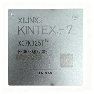
XCKU3P-2FFVA676I - Kintex UltraScale+ FPGA | AMD BGA
MPN: XCKU3P-2FFVA676I ✓ فعالXCKU3P-2FFVA676I جائزہ
A field-programmable gate array is a semiconductor whose digital logic, interfaces, and processing blocks are configured after fabrication. The FPGA product hierarchy extends from programmable logic devices to FPGAs, programmable-logic ICs, and semiconductor devices. Within the Kintex UltraScale+ family, this device provides a high-capacity implementation platform for communications, industrial control, data processing, networking, and embedded systems where hardware parallelism can improve throughput and reduce external component count.
The 355,950-cell configuration offers substantial logic capacity for designs that combine control logic, data pipelines, serial interfaces, and dedicated accelerator functions. The -2 ordering code denotes the device's speed grade, while the final I character identifies the industrial temperature option. Its BGA package provides a large number of electrical contacts compared with leaded packages, enabling extensive power, ground, configuration, and general-purpose I/O connections within a compact board footprint.
Programmable-logic designs are typically created with FPGA development tools, compiled into a configuration bitstream, and loaded into the device through a supported configuration interface. The implementation must account for the BGA's dense ball pitch, power-grid connectivity, decoupling requirements, and high-speed routing constraints. Because configuration and I/O standards are system-dependent, board designers should use the AMD package pinout files and device documentation when assigning every ball and defining power planes.
Typical uses include high-throughput signal processing, industrial automation, network-interface functions, test equipment, embedded control, and accelerator modules. The device is especially appropriate when parallel hardware architecture can outperform a sequential processor for repetitive filtering, protocol handling, or data movement. The -2 speed grade and industrial temperature marking make the part relevant to equipment expected to operate across extended industrial temperature conditions.
A critical design consideration is that the 676-ball BGA cannot be treated as a simple two-row IC footprint. Follow the AMD package pinout files, provide continuous decoupling near the device, maintain the required power and ground ball assignments, and validate escape routing before fabrication. Signal-integrity and thermal performance depend on the completed stack-up, layer count, return paths, and power-delivery network rather than on the IC alone.
This product page organizes the key electrical identity, package details, application guidance, design constraints, comparison information, and same-family migration options into a practical engineering reference. Use the manufacturer documentation for the authoritative pin assignment, complete electrical limits, configuration procedure, and design-support files before releasing a PCB or production design.
کے لیے ڈراپ اِن متبادل XCKU3P-2FFVA676I — یکساں پیکیج، پن سے پن مطابقت پذیر۔ مختلف پیکیج والے پرزے جن کے لیے PCB دوبارہ کام درکار ہو، شامل نہیں ہیں۔
اس سیریز میں مختلف ورژن
اسی سیریز کے ماڈلز جو ڈراپ اِن مطابقت رکھتے ہیں XCKU3P-2FFVA676I (یکساں فارم فیکٹر اور فٹ پرنٹ) — میں مختلف Temperature Grade.
XCKU3P-1FFVA676I
✅ ڈراپ-اِن ⚠️ تفصیلات غیر تصدیق شدہ📋 حوالہ جاتی متبادل (کیٹلاگ میں نہیں)
XCKU3P-3FFVA676I
✅ ڈراپ-اِن ⚠️ تفصیلات غیر تصدیق شدہ📋 حوالہ جاتی متبادل (کیٹلاگ میں نہیں)
XCKU3P-2FFVA676E
✅ ڈراپ-اِن ⚠️ تفصیلات غیر تصدیق شدہقیمت کے لیے رابطہ کریں
ڈیٹا شیٹ دیکھیں →XCKU3P-1FFVA676E
✅ ڈراپ-اِن ⚠️ تفصیلات غیر تصدیق شدہقیمت کے لیے رابطہ کریں
ڈیٹا شیٹ دیکھیں →XCKU3P-3FFVA676E
✅ ڈراپ-اِن ⚠️ تفصیلات غیر تصدیق شدہ📋 حوالہ جاتی متبادل (کیٹلاگ میں نہیں)
XCKU3P-2FFVA676I زیادہ سے زیادہ ریٹنگز اور برقی خصوصیات
| Device Type | Kintex UltraScale+ FPGA |
| Programmable Logic Cells | 355,950 cells |
| Logic Block Count | 20,340 CLBs |
| Architecture | Kintex UltraScale+ |
| Speed Grade | -2 |
| Temperature Grade | Industrial |
| Package Type | 676-BBGA, FCBGA |
| Total Terminals | 676 balls |
| Terminal Form | Ball |
| Package Shape | Square |
| ماؤنٹنگ ٹائپ | Surface Mount |
| Programmable Logic | Field-programmable |
| RoHS اسٹیٹس | unknown |
| REACH Status | unknown |
| AEC-Q100 Qualification | not_applicable |
XCKU3P-2FFVA676I square پن کنفیگریشن گائیڈ
XCKU3P-2FFVA676I (square پیکیج) کے لیے پن کنفیگریشن۔ اس ڈیجیٹل IC میں GPIO، کمیونیکیشن انٹرفیس (UART، SPI، I2C) اور پاور پنز شامل ہیں۔ متبادل پن فنکشنز اور کنفیگریشن آپشنز کے لیے مینوفیکچرر کے ڈیٹا شیٹ سے رجوع کریں۔ ایمبیڈڈ سسٹم ڈیزائن اور PCB لے آؤٹ کے لیے ضروری۔

کے لیے تفصیلی پن آؤٹ ڈیٹا دستیاب نہیں XCKU3P-2FFVA676I.
رجوع کریں ڈیٹا شیٹ مکمل پن کنفیگریشن کے لیے۔
عام استعمالات
XCKU3P-2FFVA676I کے لیے موزوں ہے 6 ایپلیکیشنs: Industrial Automation and Control, High-Speed Network Packet Processing, Test and Measurement Instrumentation, Industrial Signal Processing, Communications and Modem Equipment, Aerospace and Defense Control Systems.
Industrial Automation and Control
The XCKU3P-2FFVA676I fits industrial automation systems that combine machine sequencing, sensor conditioning, motion-command logic, and safety-related supervisory functions in one programmable device. Its 355,950 programmable logic cells provide substantial capacity for parallel control paths, while the -2 speed grade supports timing-sensitive logic. The 676-ball FCBGA also offers a high pin count for external interfaces. Engineers should allocate power and ground balls according to the AMD package data, use a multilayer PCB with short decoupling paths, and repeat timing and thermal analysis when the control system is upgraded with additional I/O.
High-Speed Network Packet Processing
The XCKU3P-2FFVA676I is suitable for network appliances that perform packet classification, buffering control, protocol conversion, or traffic shaping in programmable logic. A large FPGA fabric can execute many parallel operations and reduce the need for repeated processor intervention. Its 355,950-cell capacity allows designers to combine control logic and data-plane functions in one device. For a production board, the critical engineering work includes matched-length routing for high-speed interfaces, continuous reference-plane return paths, low-noise supply distribution, and careful separation of clock, data, and configuration nets.
Test and Measurement Instrumentation
XCKU3P-2FFVA676I can implement programmable logic for acquisition pipelines, pattern generation, timing control, and real-time analysis in test and measurement equipment. Hardware parallelism allows multiple channels to be processed simultaneously, while the large logic-cell count supports configurable measurement sequences and adaptive filtering. The industrial temperature marking is relevant to instrumentation deployed outside controlled laboratory environments. Designers should reserve clean clocking resources, isolate sensitive analog sections from digital activity, and verify power sequencing so that configuration and I/O rails meet the requirements of the selected AMD speed grade.
Industrial Signal Processing
The XCKU3P-2FFVA676I fits industrial signal-processing systems that perform filtering, modulation, correlation, or sensor-data transformation in parallel hardware. The 355,950-cell Kintex UltraScale+ fabric can replace chains of fixed-function logic and create a reconfigurable processing pipeline. Its -2 speed grade can improve the timing margin of demanding pipelines, although final performance remains design-specific. Engineers should use the manufacturer timing constraints, analyze pipeline latency, and confirm the operating-voltage requirements. A carefully layered PCB with grounded plane divisions and short high-speed routes helps preserve data integrity near the 676-ball device.
Communications and Modem Equipment
XCKU3P-2FFVA676I is applicable to communications equipment requiring configurable digital interfaces, framing logic, buffering, and protocol adaptation. The large BGA package provides numerous connections for high-speed data, clocks, control signals, and multiple power domains. Kintex UltraScale+ devices are commonly evaluated where parallel programmable logic can reduce external component count. The board implementation should include robust clock distribution, correctly terminated interfaces, independent decoupling around supply balls, and a power-delivery network sized for the selected device and operating corner. Signal-integrity simulation is recommended before fabrication.
Aerospace and Defense Control Systems
The XCKU3P-2FFVA676I can support configurable control, monitoring, and data-processing functions in aerospace, defense, and other mission-critical electronic systems. Its programmable architecture allows logic changes to be consolidated into one FPGA rather than multiple fixed devices, while the 355,950-cell capacity supports substantial concurrent processing. Qualification, radiation tolerance, and the applicable temperature range are not established by the basic ordering code and must be checked separately for each program. Engineers should also perform configuration-security, fault-containment, power-integrity, and environmental verification under the relevant system requirements.
کے لیے انجینئرنگ ریفرنس ڈیٹا XCKU3P-2FFVA676I — موازنہ، ڈیزائن رہنمائی، اور تعمیل کی معلومات۔
انتخاب کی گائیڈ
متبادلات کے ساتھ موازنہ
| پیرامیٹر | یہ پروڈکٹ | XCKU3P-1FFVA676I | XCKU3P-3FFVA676I | XCKU3P-2FFVA676E | XCKU3P-1FFVA676E | XCKU3P-3FFVA676E |
|---|---|---|---|---|---|---|
| Brand | AMD | AMD | AMD | AMD | AMD | AMD |
| Package | 676-BBGA, FCBGA | 676-BBGA, FCBGA - same | 676-BBGA, FCBGA - same | 676-BBGA, FCBGA - same | 676-BBGA, FCBGA - same | 676-BBGA, FCBGA - same |
| FPGA Family | Kintex UltraScale+ | Kintex UltraScale+ | Kintex UltraScale+ | Kintex UltraScale+ | Kintex UltraScale+ | Kintex UltraScale+ |
| Speed Grade | -2 | -1 | -3 | -2 | -1 | -3 |
| Temperature Suffix | I - Industrial | I - Industrial | I - Industrial | E - Extended | E - Extended | E - Extended |
| Programmable Logic Cells | 355,950 cells | 355,950 cells | 355,950 cells | 355,950 cells | 355,950 cells | 355,950 cells |
| Logic Block Count | 20,340 CLBs | 20,340 CLBs | 20,340 CLBs | 20,340 CLBs | 20,340 CLBs | 20,340 CLBs |
| Total Terminals | 676 balls | 676 balls | 676 balls | 676 balls | 676 balls | 676 balls |
اہم امتیازی خصوصیات
- Higher speed grade within the same package family (بمقابلہXCKU3P-1FFVA676I)
- Extended-temperature migration option (بمقابلہXCKU3P-2FFVA676E)
- Same-family lower-clock migration path (بمقابلہXCKU3P-3FFVA676I)
ڈیزائن نوٹس
Build the FFVA676 footprint from the AMD UltraScale package pinout files rather than a generic 676-ball BGA. Preserve all power and ground assignments, including any dedicated balls that must not be routed as ordinary signals. Check ball-pad dimensions, solder-mask definition, and assembly requirements against the current package drawing before releasing artwork.
Decouple each supply domain directly at the device balls and provide a low-impedance power-delivery network. Separate high-current and sensitive supply paths where the architecture permits, and validate voltage droop across the -2 operating corner. Power sequencing and configuration behavior must be checked against the AMD device documentation before connecting external circuitry.
Route clocks and high-speed interfaces over continuous reference planes with short vias and symmetric path lengths where source-synchronous timing applies. Keep the 676-ball escape fanout orderly, avoid routing fast signals through noisy power or switching regions, and inspect the complete stack-up with signal-integrity simulation. Configuration pins also require attention because contention or incorrect levels can prevent startup.
تعمیل کی معلومات
No explicit RoHS, REACH, lead-free, halogen-free, or conflict-minerals declarations were identified for this ordering code. AEC-Q100 is not applicable because the XCKU3P-2FFVA676I is an FPGA rather than an automotive-qualified discrete semiconductor.