IC video
Sản phẩm (50)

AD725ARZ-RL - RGB to NTSC/PAL Video Encoder | Analog Devices
The Analog Devices AD725ARZ-RL is a low-cost RGB to NTSC/PAL video encoder IC that converts red, green, and blue color component signals into their corresponding luminance and chrominance signals in accordance with either NTSC or PAL standards, housed in a 16-pin SOIC (7.50 mm width) surface-mount package delivered in tape-and-reel packaging. A video encoder is a mixed-signal device in the data conversion and video interface hierarchy that transforms parallel or analog component video (RGB or YUV) into a single composite baseband video signal, or into separate luminance (Y) and chrominance (C) signals for S-Video. Encoders sit between a graphics processor or video source and a TV monitor, VCR, or video capture input, performing the color-space conversion, subcarrier modulation, and sync generation required by broadcast television standards. Key features of the AD725 include both NTSC and PAL composite video outputs and separate chrominance and luminance (S-Video) outputs from the same device, a luminance trap (YTRAP) port that reduces cross-color artifacts generated by subcarrier-frequency components present in the luminance signal, fully TTL-compatible logic levels that support 3 V CMOS logic requirements, and an integrated luminance delay line. This combination allows a single, very low cost device to serve as the complete analog video output stage for embedded systems. Technically, the AD725 performs RGB-to-YUV matrix conversion, quadrature modulation of the color difference signals onto a subcarrier, and sync insertion, producing standard-amplitude baseband video. For portable or other power-sensitive applications, the device can be powered down to less than 1 uA of current consumption, which is exceptionally low for a video-grade mixed-signal encoder. Typical applications include embedded graphics boards, set-top box video outputs, industrial display interfaces, legacy TV-out ports on microprocessor systems, and video test equipment where NTSC or PAL composite output is required from an RGB source. A key design consideration is proper use of the YTRAP pin: connecting the correct external LC trap circuit suppresses subcarrier leakage into the luminance path and materially reduces cross-color shimmer on fine luma detail. Supply decoupling and standard-accuracy crystal reference for the color subcarrier are also important for color accuracy. This page synthesizes distributor pricing, drop-in alternatives, practical design notes, and application guidance not found in the manufacturer datasheet alone.
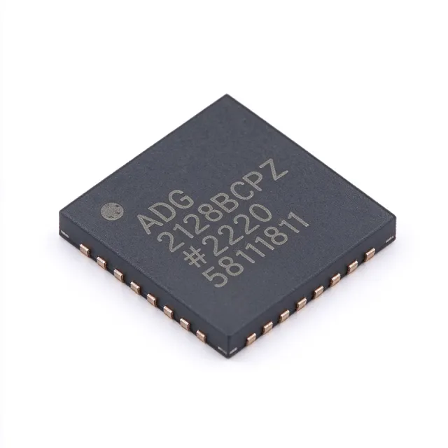
ADG2188BCPZ - 8x8 Analog Crosspoint Switch | Analog Devices
The ADG2188BCPZ is an 8x8 analog crosspoint switch from Analog Devices, designed for routing analog signals in telecommunications, ultrasound, and audio applications. It features 64 bidirectional switch channels arranged in an 8x8 array, with each switch individually addressable via an I2C-compatible interface. The device operates from a single 3.3V or 5V supply and is available in a 32-lead LFCSP-VQ (5x5 mm) package. An analog crosspoint switch is a matrix of switches that connects any input to any output, enabling flexible signal routing without external wiring. It is a key building block in signal routing systems, allowing multiple signals to be directed to different destinations under software control. The ADG2188 belongs to the family of analog switches and multiplexers, which are essential in applications requiring signal distribution and switching. Key features include low on-resistance, low leakage currents, and high bandwidth, ensuring minimal signal distortion. The I2C interface supports standard, full, and fast modes, allowing easy integration with microcontrollers. The device also includes an address pin for multiple device configuration on the same bus, and a reset pin for initialization. Technically, the ADG2188 uses CMOS technology to achieve low power consumption and high switching speed. The switch array is bidirectional, meaning rows and columns can be configured as inputs or outputs, providing flexibility in signal routing. The device also features break-before-make switching to prevent momentary short circuits during channel changes. Typical applications include telecommunications switching, ultrasound imaging, audio routing, and automatic test equipment. In telecommunications, it can route multiple channels in a central office; in ultrasound, it can switch transducer elements; in audio, it can route signals in mixing consoles. When designing with the ADG2188, ensure proper decoupling of the power supply and careful layout to minimize crosstalk. The I2C address pins should be set correctly to avoid bus conflicts. The device is RoHS compliant and suitable for surface-mount assembly.

ADG2188BCPZ-RL7 - 8x8 Analog Crosspoint Switch | Analog Devices
The ADG2188BCPZ-RL7 is an I2C CMOS 8x8 unbuffered analog switch array from Analog Devices, designed for routing analog signals in telecommunications, ultrasound, and audio applications. It provides 64 bidirectional switch channels arranged in eight columns by eight rows, with each switch individually addressable via a standard I2C-compatible interface. The device operates from dual or single supplies, supporting a wide analog signal range, and is housed in a compact 32-lead LFCSP-VQ (5x5 mm) package. An analog crosspoint switch is a type of analog switch array that allows any input to be connected to any output, enabling flexible signal routing without mechanical relays. It is a key building block in signal routing and switching systems, sitting between discrete analog switches and full digital crosspoint ICs in the signal chain hierarchy. The ADG2188's 8x8 matrix provides a balance of channel count and package size, making it suitable for dense PCB designs. Key features include a low on-resistance of [DATA_NEEDED: on-resistance] ohms, low leakage currents, and a wide operating voltage range. The I2C interface supports standard and full-speed modes, allowing easy integration with microcontrollers. The device also features a reset pin and address pins for multiple device configuration on the same bus. Its bidirectional architecture simplifies PCB layout by allowing rows and columns to be configured as inputs or outputs. Technically, the ADG2188 uses CMOS technology to achieve low power consumption and high signal integrity. The unbuffered architecture preserves signal fidelity, making it ideal for precision analog applications. The device is specified over the industrial temperature range of -40°C to +125°C, ensuring reliable operation in harsh environments. Typical applications include telecommunications switching, ultrasound imaging systems, audio routing, and automated test equipment. In ultrasound, the ADG2188 routes transducer signals to processing channels, while in audio, it enables flexible mixing and routing. Its low distortion and high bandwidth make it suitable for high-frequency signals. When designing with the ADG2188, ensure proper decoupling on the supply pins and consider the on-resistance flatness for precision applications. The I2C address pins allow up to [DATA_NEEDED: number of addressable devices] devices on a single bus, enabling large switch matrices.

ADV202BBCZ - JPEG2000 Video Codec | Analog Devices
The ADV202BBCZ is a single-chip JPEG2000 video codec from Analog Devices, designed for real-time compression and decompression of standard-definition video streams. It supports 16-bit parallel input/output and operates at a maximum clock frequency of 150 MHz, enabling high-throughput processing for broadcast and professional video applications. The device is housed in a 144-ball CSPBGA package (13x13 mm) and operates from a 1.8V core supply with 3.3V I/O, making it suitable for power-sensitive embedded systems. A video codec is a hardware or software component that encodes (compresses) and decodes (decompresses) digital video. The ADV202 implements the JPEG2000 standard (ISO/IEC 15444-1), which uses wavelet-based compression to achieve high image quality at low bit rates. As a dedicated codec IC, it offloads computationally intensive processing from host processors, enabling real-time video streaming in applications such as broadcast infrastructure, medical imaging, and surveillance systems. Key features include support for both lossy and lossless compression, programmable compression ratios, and a flexible host interface that supports both parallel and serial (SPI) modes. The device also includes an internal DMA controller for efficient data transfer, and its low power consumption (typically 1.5W) makes it ideal for portable and embedded designs. The ADV202BBCZ is part of the ADV202 family, which includes speed grades of 115 MHz and 150 MHz, with the BBCZ suffix indicating the 150 MHz version in a CSPBGA package. Technically, the ADV202 integrates a wavelet transform engine, an entropy coder, and a rate control unit on a single die. It accepts raw video data in various formats, including YCbCr 4:2:2 and 4:4:4, and outputs compressed JPEG2000 streams. The device supports resolutions up to 720x576 (D1) at 30 fps, making it suitable for standard-definition video processing. Its architecture allows for low-latency encoding, which is critical for real-time applications. Typical applications include video surveillance systems, medical imaging devices, broadcast video servers, and digital cinema. The ADV202BBCZ is also used in military and aerospace systems for secure video transmission. Its robust design and long-term availability make it a preferred choice for industrial and professional video equipment. When designing with the ADV202BBCZ, ensure proper decoupling of the 1.8V core supply and 3.3V I/O supply, and follow the recommended PCB layout guidelines in the datasheet to minimize noise and ensure signal integrity. The device requires an external clock source and configuration via its host interface before video processing can begin.
ADV202BBCZ-RL - JPEG2000 Video Codec | Analog Devices
The ADV202BBCZ-RL is a single-chip JPEG2000 video codec from Analog Devices, designed for real-time compression and decompression of video streams. It supports a 16-bit interface and operates at a clock speed of up to 150 MHz, enabling high-throughput processing for broadcast and professional video applications. The device is housed in a 144-ball CSPBGA package (13x13 mm), offering a compact solution for space-constrained designs. A video codec is an integrated circuit that encodes and decodes digital video signals, converting raw video data into compressed formats for efficient storage and transmission. The ADV202BBCZ-RL specifically implements the JPEG2000 standard, which uses wavelet-based compression to deliver superior image quality at high compression ratios. This codec sits within the broader category of multimedia processors, bridging raw video capture and digital transmission systems. Key features of the ADV202BBCZ-RL include support for JPEG2000 Part 1, a 16-bit host interface, and a maximum clock frequency of 150 MHz. The device offers low power consumption, making it suitable for portable and embedded systems. Its 144-ball CSPBGA package provides excellent thermal performance and a small footprint, ideal for dense PCB layouts. Technically, the ADV202BBCZ-RL integrates a wavelet transform engine, entropy coder, and rate control logic on a single die. This architecture enables real-time encoding and decoding of high-definition video without external processing. The device supports multiple resolution levels and quality layers, allowing flexible bitrate control for various applications. Typical applications include broadcast video servers, medical imaging systems, surveillance DVRs, and digital cinema equipment. The codec's high throughput and low latency make it well-suited for real-time video processing where image fidelity is critical. When designing with the ADV202BBCZ-RL, ensure proper decoupling of the power supply pins and follow the recommended layout guidelines in the datasheet to minimize signal integrity issues. The device requires a clean clock source and careful attention to thermal management due to its high-speed operation.

ADV3203ASWZ - 300 MHz 32x16 Buffered Crosspoint | Analog Devices
Analog Devices ADV3203ASWZ is a 300 MHz, 32 x 16 buffered analog crosspoint switch with a 176-lead LQFP exposed-pad package, a gain of +2, and a selectable sync-tip clamp input. The integrated routing matrix provides nonblocking signal paths for high-density analog video applications, while a 2:1 on-screen display insertion multiplexer supports OSD integration at each output. The device accepts single +5 V, dual ±2.5 V, or dual ±3.3 V supply arrangements when operating with the specified gain. An analog crosspoint switch is a matrix of buffered inputs and outputs that can route multiple signals through independently selected connections. In the product hierarchy, the ADV3203ASWZ is an analog crosspoint switch, a specialized interface IC, and ultimately a semiconductor designed for high-density routing. Unlike mechanical or passive matrix devices, it combines programmable routing, active buffering, signal isolation, and OSD insertion in one integrated circuit. Key performance features include 300 MHz operating bandwidth, 0.1 dB gain flatness through 60 MHz, -48 dB crosstalk at 5 MHz, and -80 dB isolation at 5 MHz. These characteristics support routing of wideband composite or component video signals where amplitude consistency and rejection of unwanted paths are important. The buffer also provides high-impedance output disable, allowing multiple devices to be connected for expanded routing capacity with minimal output-loading interaction. The internal architecture provides 32 x 16 nonblocking switching, a +2 video gain stage, and a selectable sync-tip clamp suitable for AC-coupled signal paths. Serial programming controls the switch array, reducing the number of control connections required by a large routing system. A separate 2:1 OSD insertion mux is available per output, allowing graphics or overlay information to be combined with the primary routed video path. Typical applications include professional video routers, broadcast production equipment, audiovisual distribution systems, presentation equipment, surveillance-video switching systems, and industrial monitoring panels. The 176-lead LQFP package with exposed pad supports high-density PCB routing while requiring careful thermal design because it contains many active buffered switching paths. Layout should preserve short analog traces, provide clean supply distribution, and place decoupling close to the supply pins. Because the exposed pad is an electrical and thermal connection, its PCB implementation must follow the package guidance. Signal-integrity checks should include return loss, gain flatness, crosstalk, isolation, and output-disable behavior across the intended video bandwidth. This page combines verified manufacturer information, distributor availability and pricing, same-family alternatives, and application-oriented design guidance. It distinguishes directly related family members from broad cross-reference search tools and identifies unavailable pin-level or qualification data rather than estimating it.

ADV3205JSTZ - 60 MHz Buffered Analog Crosspoint | Analog Devices
Analog Devices ADV3205JSTZ is a fully buffered analog crosspoint switch matrix designed for video signal routing. The device provides a 16 × 16 switch arrangement, a specified signal bandwidth of 60 MHz, and a gain of +2 dB. It operates from ±5 V according to the manufacturer description, making it suitable for systems that need buffered analog routing with controlled impedance and improved signal isolation. The ADV3205JSTZ is identified in distributor data as a one-channel video switch IC in a 100-lead LQFP package measuring 14 mm × 14 mm. An analog crosspoint switch is a semiconductor routing matrix that connects one source signal to one destination while buffering the selected path. Unlike an unbuffered passive matrix, the ADV3205 provides active buffering, which can reduce loading effects and support controlled signal transfer between source and destination stages. In a broader equipment hierarchy, it belongs to the analog switch and signal-routing category, within interface and video-routing applications. Its buffered architecture is particularly relevant when the routed signal must remain useful across multiple video-processing stages. The principal verified performance characteristics are 60 MHz signal bandwidth, +2 dB gain, a 16 × 16 matrix, operation from ±5 V, and channel switching time below 60 ns with 0.1% settling. The switching-time figure indicates how quickly the device changes routing state, while the settling specification describes the time required for the output to reach the specified accuracy. The low settling behavior can be valuable in measurement, broadcast, test-equipment, and video-processing systems where a new source must be selected quickly. The ADV3205 also includes ground and power pins around the inputs and outputs to provide shielding between signal paths. This arrangement is intended to improve isolation for demanding analog-routing applications and can reduce coupling between adjacent channels when the PCB layout and grounding system are implemented carefully. The manufacturer identifies the device as recommended for new designs and markets it for video applications, so it is positioned as an active analog-routing solution rather than a simple discrete switch. Typical uses include professional video routing, camera and monitor signal distribution, laboratory test systems, broadcast equipment, and industrial video control. In these systems, the matrix can route one of multiple source signals to a processing chain or measurement instrument. The active buffering helps maintain signal integrity when routing is combined with downstream amplifiers, converters, or acquisition circuits. Because the verified material does not provide the complete electrical table, exact input impedance, output impedance, channel resistance, power consumption, temperature range, and detailed pin functions cannot be independently confirmed from the supplied sources. Designers should place supply decoupling close to the analog IC and preserve the manufacturer’s recommended grounding and shielding topology around the input and output groups. The 14 mm × 14 mm LQFP package also requires adequate PCB escape routing and thermal consideration for high-frequency signal integrity. The verified distributor pages provide the product identity, package information, headline bandwidth, gain, supply arrangement, and switching behavior; final production design should therefore be validated against the complete Analog Devices datasheet, including absolute maximum ratings, recommended operating conditions, and the complete pinout. This page consolidates the supplied manufacturer and distributor information, practical routing considerations, application guidance, and verified-source links. It distinguishes documented headline specifications from fields that still require confirmation from the full datasheet rather than inferring values that were not provided in the verified data.

ADV3229ACPZ - 750 MHz 8x8 Crosspoint Switch | Analog Devices
Analog Devices ADV3229ACPZ is a high-speed, nonblocking 8 x 8 analog crosspoint switch with a 750 MHz bandwidth, +2 gain output amplifiers, and a 72-lead LFCSP-VQ package measuring 10 x 10 mm. It supports buffered inputs, programmable high-impedance outputs, and drives of 150 ohm loads while operating from positive and negative 5 V supplies. An analog crosspoint switch is a multi-input, multi-output routing matrix that connects any selected input channel to any selected output channel without requiring the inactive channels to terminate. Within the semiconductor hierarchy, the ADV3229ACPZ is an analog switch IC, an interface IC, and a signal-routing device for high-frequency video, telecommunications, broadcast, and test equipment. Its nonblocking architecture allows supported channels to remain active while other crosspoint routes change. Key features include an 8 x 8 switch array, eight buffered inputs, eight programmable high-impedance outputs, and eight output amplifiers configured for a gain of +2. The device is specified for 150 ohm loads and low power consumption of 0.5 W. According to the Analog Devices ADV3228/ADV3229 data sheet, its large-signal bandwidth is 750 MHz and its slew rate is 2500 V/us. Technically, the ADV3229 integrates routing switches, input buffers, output amplifiers, and output-disconnect functions into one high-speed analog matrix. The +2 output gain differentiates it from the otherwise closely related ADV3228, which uses +1 gain. The data sheet also identifies the ADV3229 as pinout- and functionally equivalent to the AD8108 and AD8109, making those legacy devices important references when evaluating board compatibility. Typical uses include professional video routing, broadcast video distribution, telecommunications test systems, high-definition signal routing, and instrumentation requiring repeatable high-bandwidth channel selection. The buffered inputs help isolate upstream sources, while the programmable output high-impedance states allow unused outputs to be isolated from driven channels. Designers should verify control-logic levels, exposed-pad grounding, bypass-capacitor placement, and signal-integrity performance on the target board. The 10 x 10 mm land pattern and high-speed analog routing require short connections, a continuous ground reference, and careful control of supply-return paths. Because the ADV3229 uses dual-rail supplies, both positive and negative rails must be present with appropriate decoupling. This page consolidates manufacturer features, distributor pricing, verified source links, same-family drop-in alternatives, and practical selection guidance. It also distinguishes confirmed pin-compatible options from legacy functionally equivalent devices so engineers can verify every footprint, gain, and control requirement before redesigning an existing PCB.
ADV7171KS - 10-Bit PAL/NTSC Video Encoder | Analog Devices
The Analog Devices ADV7171KS is an integrated digital PAL/NTSC video encoder with a 10-bit DAC and advanced power management, packaged in a 44-lead MQFP. According to the manufacturer product page, it converts Digital CCIR-601 4:2:2 8-bit or 16-bit component video data into a standard analog baseband television signal compatible with worldwide standards. The encoder is designed for DVD playback systems, portable video equipment, digital still cameras, laptop PCs, video games, and PC video or multimedia systems. A digital video encoder is an interface and signal-conversion IC that accepts parallel digital video, applies encoding and color-processing functions, and generates composite or component analog video suitable for display equipment. Its role in the signal chain is between a digital video source and an analog display or broadcast interface. The ADV7171 family supports serial control through a 2-wire I2C-compatible interface and uses two slave addresses, allowing configuration of operating modes and encoder functions from a host controller. The key verified feature set includes Digital CCIR-601 4:2:2 input support in either 8-bit or 16-bit formats, a 10-bit DAC, PAL and NTSC encoding capability, and advanced power management. The Analog Devices family description identifies the device as an integrated digital video encoder rather than a general-purpose processor. Its 44-lead MQFP package provides a defined gull-wing footprint for conventional surface-mount PCB assembly and is available in industrial-temperature component listings. The ADV7171KS is appropriate when a design must preserve a digital video source while producing standard analog baseband output. The serial control interface simplifies integration with source-specific firmware, while the dedicated video encoder reduces the need for external DAC and encoding circuitry. Engineers should still verify clocking, sync polarity, pixel clock relationships, output loading, power sequencing, and analog video quality against the complete manufacturer datasheet before releasing a production layout. Typical applications include DVD playback systems, portable video equipment, digital still cameras, laptop computers, video games, and PC video or multimedia products. In these systems, the encoder can convert decoded digital video into PAL or NTSC-compatible analog signals for downstream display or capture equipment. The dedicated encoder also supports integration into compact consumer products where board area and external component count are important. A key design consideration is that analog baseband video requires careful PCB layout and signal-integrity control. Keep the encoder clock and digital-video traces away from sensitive output paths, provide clean power and ground connections, and follow the manufacturer’s recommended decoupling and output-network details. Because the supplied web data does not expose the complete electrical timing table, pin names, or exact operating limits, those values should not be inferred from generic video-encoder specifications. This page consolidates verified manufacturer and distributor information, including the ADV7171KS application context, package identity, family capabilities, and replacement-search results. It is intended to support component selection and engineering research while clearly separating verified facts from parameters that still require confirmation in the complete ADV7170/ADV7171 datasheet.

ADV7171KSU 10-Bit PAL/NTSC Video Encoder | Analog Devices
Analog Devices ADV7171KSU is an integrated 10-bit digital video encoder that converts ITU-R BT.601/656 YCrCb 4:2:2 component data into standard PAL or NTSC analog baseband video. The device provides four video DAC outputs and is supplied in a surface-mount 44-pin TQFP package measuring 10 mm by 10 mm. Its primary function is to bridge a digital video source and legacy analog composite, S-Video, or component outputs. A video encoder is a signal-conversion semiconductor that accepts digital pixel data and generates an analog waveform accepted by PAL or NTSC display equipment. Within the product hierarchy, the ADV7171 is an interface IC and video encoder rather than a processor or display driver. The corresponding digital-video-to-analog-video conversion stage sits between a video source, such as a DVD controller or multimedia processor, and an analog video connector or display. According to the Analog Devices ADV7171 product page, the encoder supports 8-bit or 16-bit CCIR-601 4:2:2 component video input. Its four 10-bit DACs support PAL and NTSC generation, while its digital video input follows the BT.601/656 format identified in the provided product information. This integration reduces the need for external video DACs when a design requires both S-Video and composite or additional analog video outputs. The ADV7170 and ADV7171 family is positioned for high-performance DVD playback, portable video equipment, digital still cameras, laptop computers, video games, and PC video or multimedia systems. The supplied search data does not provide verified clock frequency, power-supply range, output voltage resolution, operating temperature, timing limits, or package dimensions beyond the 10 mm by 10 mm TQFP description, so those values are not inferred here. The main engineering concern is interface compatibility rather than power conversion. The source must supply correctly timed BT.601/656 YCrCb data, the PCB must route high-speed digital video signals without excessive distortion, and analog outputs must be terminated according to the selected PAL or NTSC standard. The exact clocking, synchronization, control-register, and DAC configuration procedure must be taken from the manufacturer data sheet rather than inferred from the order code. For procurement, ADV7171KSUZ and ADV7171KSUZ-REEL appear in the supplied cross-reference results as the same 44-pin device with compatible terminals and characteristics, but the KSUZ order codes may represent ordering or reel-packaging conventions rather than five distinct functional alternatives. This page therefore distinguishes verified function-level choices from packaging suffixes and does not present reel-code variants as separate engineering options. This page consolidates the supplied manufacturer description, distributor package information, cross-reference findings, application guidance, and unresolved-data warnings. It is intended to support engineering selection and sourcing while directing readers to the manufacturer data sheet for authoritative electrical limits, pin functions, register definitions, and timing specifications.
ADV7171KSZ - PAL/NTSC Video Encoder | Analog Devices
Analog Devices ADV7171KSZ is an integrated digital PAL/NTSC video encoder with a 10-bit SSAF architecture and advanced power management, supplied in a 44-MQFP package measuring 10 x 10 mm. The device accepts digital CCIR-601 4:2:2 component video in either 8-bit or 16-bit form and converts it into a standard analog baseband television signal compatible with worldwide PAL and NTSC systems. An integrated video encoder is a signal-processing IC that bridges a digital video pipeline and an analog composite or component output. In the product hierarchy, the ADV7171 belongs to video codecs and converters, within interface ICs, rather than acting as a general-purpose processor or display driver. Its principal purpose is to preserve useful picture information while translating digital video data into the modulation and level characteristics required by legacy analog television equipment. Three headline characteristics define the ADV7171KSZ: 10-bit SSAF video conversion, digital PAL/NTSC encoding, and operation from a 4.75 V to 5.25 V analog supply. The 4.75 V to 5.25 V supply range supports conventional 5 V equipment designs, while the 44-MQFP package provides 44 externally accessible connections for digital data, control, clocking, power, and analog output functions. The manufacturer describes the family as suitable for high-performance DVD playback, portable video equipment, digital still cameras, laptop PCs, video games, and PC multimedia systems. Advanced power management is a central feature of the device family. According to the Analog Devices ADV7170/ADV7171 datasheet, the encoder can use its SCRESET/RTC pin together with Mode Register 2 bits MR22 and MR21 to lock to an external video source. The real-time control mode automatically alters the subcarrier frequency to compensate for line-length variation. These functions allow an encoder to remain synchronized with an external source when its timing differs from the nominal internal reference. Typical implementations place the ADV7171KSZ between a digital video source and an analog video connector or downstream display. A DVD player can feed decoded video into the encoder for compatibility with a PAL or NTSC television. Portable equipment can use the same conversion function when an analog video output is required, while PC video and multimedia designs use it as a bridge from digital graphics or decoded video to an external analog display. The primary design consideration is that the ADV7171KSZ is a legacy-standard bridge rather than a modern HDMI or display-port transmitter. Designers must confirm signal timing, input word width, output standard, synchronization behavior, and analog output integration before layout release. The Analog Devices product page marks the ADV7171 as not recommended for new designs, so new products should evaluate current encoder options unless legacy equipment requires exact compatibility. This page combines manufacturer capabilities, distributor availability, package information, lifecycle status, and verified replacement candidates. It also identifies where pin-level and pricing information remains unavailable, helping engineers distinguish confirmed device data from details that must be checked against the official datasheet and authorized distribution channels.
ADV7176AKS - 10-Bit 4-DAC PAL/NTSC Video Encoder | Analog Devices
The Analog Devices ADV7176AKS is an integrated 10-bit digital CCIR-601 component-video encoder with four DACs, designed to convert 8-bit or 16-bit 4:2:2 YCrCb data into PAL or NTSC analog baseband video. It is supplied in a 44-pin MQFP package and is intended for professional video equipment, broadcast conversion systems, digital video processors, and other applications requiring deterministic component-video encoding. A video encoder is an interface and signal-conversion device that translates digital component-video data into a legacy analog baseband format accepted by PAL and NTSC equipment. Within the broader product hierarchy, the ADV7176AKS is a video encoder IC, a signal-conversion integrated circuit, and ultimately a semiconductor used within professional video and broadcast equipment. Its CCIR-601 input interface and four analog output DACs consolidate digital-to-analog video conversion into one device. The principal verified feature set includes 10-bit conversion, four DAC outputs, CCIR-601 4:2:2 input, and support for PAL B/D/G/H/I, PAL M, PAL N, and NTSC. Teletext insertion is identified in the verified product listing for the ADV7176AKS. These features make the device relevant where component-video data must be converted into standard analog television signals without relying on a collection of discrete output converters. The 44-pin MQFP package provides 44 electrical connections for digital-video input, clock and control signaling, analog output channels, power, ground, and configuration functions. Exact pin names, voltage ratings, clock requirements, DAC output ranges, and absolute maximum ratings are not included in the supplied source excerpts; engineers should therefore use the Analog Devices ADV7176/ADV7176A manufacturer datasheet for implementation details rather than infer missing values from the family description. Typical uses include PAL/NTSC video recording equipment, professional broadcast and post-production systems, digital-video test equipment, video standards-conversion products, and embedded television interfaces. The part accepts digital data upstream and produces analog baseband outputs downstream, making it suitable for equipment that must bridge modern digital processing with installed analog video infrastructure. The most important design consideration is that this is an obsolete product, so new production designs should account for lifecycle risk, limited supply, and obsolete-product support constraints. Hardware redesign should begin by checking the complete pinout, electrical limits, synchronization requirements, DAC loading, and reference circuitry in the manufacturer datasheet. PCB layout should preserve short analog output paths and controlled digital-clock routing to reduce conversion-quality and timing risks. This page consolidates verified lifecycle information, package details, functional characteristics, source links, and replacement-analysis constraints. It also distinguishes documented functions from unavailable electrical parameters and does not present unverified substitute parts as guaranteed drop-in replacements.

ADV7179BCP - 10-Bit NTSC/PAL Video Encoder | Analog Devices
Analog Devices ADV7179BCP is a 10-bit chip-scale NTSC/PAL analog video encoder with three DAC outputs in a 40-LFCSP-WQ (6x6 mm) exposed-pad package. It accepts digital CCIR-601 4:2:2, 8-bit component-video data and converts it into a standard analog baseband television signal. Its identified operating supply is 3.3 V, with guaranteed timing specifications from 3.0 V to 3.6 V. A video encoder is a signal-conversion integrated circuit that transforms digital video into legacy analog composite or component output. In the product hierarchy, the ADV7179BCP is a video encoder, interface IC, signal-processing semiconductor, and communications-interface component. It bridges a digital video pipeline and displays or capture equipment that still require NTSC or PAL baseband signals. Key features include three 10-bit DACs, support for PAL and NTSC systems, a 40-LFCSP-WQ package with an exposed pad, and a stated operating temperature range of -40°C to +85°C. According to the Analog Devices ADV7174/ADV7179 data sheet, the timing specifications apply with a 3.3 V analog supply, a 1.235 V reference, and a 150 Ω RSET resistor. The encoder also supports WSS and CGMS-A data control generation. The digital input follows the CCIR-601 4:2:2, 8-bit component-video format, while the encoder generates synchronized analog baseband outputs. Output video frames are synchronized with incoming timing reference codes. Optionally, the device accepts or generates HSYNC, VSYNC, and FIELD timing signals, and those pulse widths and positions can be adjusted in master mode. Master and slave timing behavior therefore supports integration with different video timing sources. Typical uses include legacy broadcast and surveillance equipment, industrial inspection systems, video capture cards, camera interfaces, mobile or portable video products, and embedded systems requiring an analog NTSC or PAL output from a CCIR-601 digital-video source. The three DAC outputs support the device's role as a complete integrated encoder rather than a digital-only processing block. Designers should preserve the documented supply range, reference configuration, and external RSET value of 150 Ω. The exposed pad requires careful thermal and layout treatment so heat can leave the encoder package, while analog video outputs require suitable termination and trace-impedance control to avoid signal degradation. This page consolidates manufacturer functionality, verified pricing, lifecycle information, package details, and application-focused design guidance. It also distinguishes documented ADV7179 family alternatives from unrelated cross-package parts so engineers can evaluate replacement options without assuming that similar encoder functions guarantee pin-to-pin compatibility.

ADV7181BCP - Multiformat Video Decoder | Analog Devices
The Analog Devices ADV7181BCP is a multiformat SDTV video decoder that automatically detects and converts NTSC, PAL, and SECAM analog baseband television signals into 8-bit precision 4:2:2 component-video data. The device integrates three 54 MHz, 9-bit ADCs clocked from a single 27 MHz crystal and is supplied in a 64-lead LFCSP-VQ package measuring 9 mm by 9 mm. It is intended for video capture, processing, and display systems that require automatic analog-format recognition. A video decoder is an interface IC within the broader video-processing hierarchy. It receives composite, S-Video, or supported component-video signals, digitizes the analog waveforms, extracts luminance and chrominance information, and presents the decoded result to a digital video pipeline. The ADV7181BCP therefore sits between legacy analog video sources and digital processors, displays, recorders, and transmission equipment. Key features include automatic NTSC, PAL, and SECAM detection, three integrated 9-bit ADCs, and a common 27 MHz crystal reference. The decoder supports the NTSC-M, NTSC-N, and NTSC-4.43 variants identified in the retrieved manufacturer information, along with PAL-B, PAL-D, PAL-G, PAL-H, PAL-I, PAL-M, and PAL-N. Its 8-bit 4:2:2 output provides a practical digital component-video interface for downstream processing. ADI describes the ADV7181 as a new-generation integrated video decoder using Adaptive Digital Line Length Tracking, or ADLLT. This technology is intended to improve digital video capture, processing, and display performance by automatically adapting the decoder to varying analog line lengths. The integrated ADCs reduce the number of separate data converters required in an analog-video front end while centralizing synchronization around one crystal source. Typical uses include SDTV capture equipment, set-top boxes, video recorders, industrial monitoring systems, broadcast processing, and consumer display products. In a composite-video design, the analog input is routed to the decoder and the resulting digital video is passed to a scaler, image processor, display controller, or storage device. Engineers must still verify voltage levels, timing, exposed-pad layout, analog input conditioning, and software-register compatibility against the manufacturer datasheet. A critical design consideration is that this highly integrated decoder does not eliminate the need for careful PCB implementation. Analog inputs should be routed away from digital clocks and switching nodes, while the exposed pad requires the datasheet-recommended thermal and electrical layout. Input filtering, grounding, power sequencing, and crystal-layout guidance should be followed directly rather than inferred from generic video-decoder practice. This page consolidates the verified manufacturer description, distributor availability information, same-family alternatives, comparison parameters, and practical selection guidance. It also distinguishes documented specifications from unresolved supply, electrical, timing, and lifecycle details rather than estimating missing values.

ADV7181BST Multiformat SDTV Video Decoder | Analog Devices
Analog Devices ADV7181BST is a multiformat standard-definition television video decoder IC that automatically detects NTSC, PAL, or SECAM analog baseband signals and converts them into 8-bit precision 4:2:2 component video data. It is supplied in a 64-lead LQFP surface-mount package and is designed for digital video capture, processing, and display systems requiring compatibility with worldwide analog television standards. An analog video decoder is an interface IC that recovers timing and separates luminance and chrominance information from a composite or component baseband video signal. Within the semiconductor hierarchy, the ADV7181BST is a video interface IC, decoder IC, and signal-processing semiconductor. Its decoded output uses the 4:2:2 component format and is compatible with 8-bit and 16-bit CCIR601 or CCIR656 digital video interfaces. The principal feature is automatic detection of NTSC, PAL, and SECAM standards, reducing the need for separate decoders or extensive manual mode configuration. The device accepts standard analog baseband television signals and produces digital component-video data suitable for subsequent scaling, processing, encoding, capture, or display. This combination makes it useful in professional video equipment, television receivers, video capture systems, surveillance equipment, industrial imaging systems, and legacy audiovisual installations. Analog Devices describes the ADV7181 as using ADLLT, or Adaptive Digital Line Length Tracking, technology. According to the manufacturer product information, this technology provides advantages for digital video capture, processing, and display applications. A more recent ADV7181B product page states that its B revision improves performance for noisy or weak signal inputs and improves VCR locking capability. Those revision-level improvements should not automatically be attributed to ADV7181BST without checking the exact ordering code and its datasheet revision. The ADV7181BST operates as a high-volume analog-to-digital video interface function. Designers must provide suitable analog input routing, stable supply rails, compliant clocking, and an appropriate digital output destination. Because this is a multiformat legacy-standard decoder rather than a modern compressed-video processor, it is most appropriate where an equipment block still receives NTSC, PAL, or SECAM baseband video and requires standardized digital component-video output. For implementation, pin assignment, supply voltage, clock requirements, and analog input configuration should be taken directly from the manufacturer documentation for the exact ADV7181BST ordering code. The available web information confirms the decoder function, supported standards, output format, digital-interface compatibility, package family, and ADLLT technology, but it does not provide a complete electrical characteristic table or verified operating limits. Those details should therefore be confirmed before schematic capture, timing design, or production release. This page synthesizes the verified manufacturer description, distributor pricing indication, package information, and drop-in-family comparison data to support engineering selection. It distinguishes confirmed ADV7181BST capabilities from unverified electrical parameters and highlights the limited number of pin-compatible replacements supported by the supplied cross-reference results.
ADV7191KST - 6-Channel 10-Bit Video Encoder | Analog Devices
Analog Devices ADV7191KST is an integrated digital video encoder with six 10-bit DAC outputs and 54 MHz oversampling, packaged for professional analog-video signal conversion. It accepts digital CCIR-601 4:2:2 component video data in 8-bit or 16-bit format and produces standard analog baseband television signals compatible with NTSC, PAL B/D/G/H/I, PAL M, PAL N, and PAL-60 systems. The device combines a digital video encoding core with programmable luminance and chrominance filters plus multiple analog output channels. A video encoder is a signal-conversion integrated circuit that transforms digital component-video data into analog composite, component, or related baseband outputs. Within the broader semiconductor hierarchy, the ADV7191KST belongs to the video encoder and interface IC family, where it bridges digital video processing systems and legacy analog broadcast equipment. Its integrated DACs reduce the number of separate converters required in professional video signal paths. The principal features include six 10-bit DAC outputs, 54 MHz oversampling, support for 8-bit and 16-bit CCIR-601 4:2:2 input, and programmable luminance and chrominance filtering. The manufacturer describes the ADV7190 and ADV7191 as functionally equivalent, with the ADV7190 additionally incorporating the Macrovision Revision 7 anti-copy algorithm. The ADV7191 therefore favors systems that need the encoder architecture without that specific Macrovision feature. The converter is designed for digital-video equipment that must generate multiple analog television outputs while preserving programmable filtering control. Its 10-bit DAC resolution provides 1024 theoretical quantization levels per output, while 54 MHz oversampling supports filtered analog reconstruction. Because the six outputs are integrated, board designers can reduce external DAC count while retaining separate baseband signal paths where the application requires them. Typical uses include broadcast and studio video conversion, professional monitoring, video test and measurement equipment, industrial imaging, video-distribution racks, and legacy analog-video interfaces connected to digital processing. System-level qualification should include checking supported video timing, output bandwidth, synchronization behavior, and external analog-filter requirements against the manufacturer datasheet before releasing a production design. The most important design consideration is preserving the intended analog signal path. DAC output filtering, ground-plane continuity, power-supply decoupling, and clock or synchronization layout can materially affect output quality. Designers should follow the manufacturer’s recommended application circuit and verify their external component values rather than inferring values from this overview. This page consolidates the verified manufacturer description, source links, packaging constraints, drop-in alternatives, application guidance, and engineering trade-offs for engineers evaluating the ADV7191KST. It adds design-oriented context beyond a distributor listing while clearly separating verified facts from data requiring confirmation from the full datasheet.

ADV7194KST - 54 MHz Extended Video Encoder | Analog Devices
Analog Devices ADV7194KST is an integrated professional extended-10 video encoder with 54 MHz oversampling, packaged in an 80-lead LQFP. It converts digital CCIR-601 4:2:2 component-video data at 8-, 10-, 16-, or 20-bit resolution into standard analog baseband television signals compatible with NTSC, PAL B/D/G/H/I, PAL N, and PAL-60. The encoder supports 8-, 10-, 16-, and 20-bit digital input widths and operates as a surface-mount video encoder IC. A video encoder is a signal-conversion semiconductor that transforms digital component-video data into a standardized analog television output. Within the broader signal-chain hierarchy, the ADV7194 belongs to video encoding and decoding ICs, multimedia processors, interface ICs, and ultimately semiconductors. Its digital inputs accept formatted CCIR-601 component-video streams, while its analog outputs recreate luminance and chrominance signals suitable for conventional broadcast, video-production, DVD, PC-video, and multimedia equipment. Key features include 54 MHz oversampling, support for eight input word lengths, and compatibility with multiple analog television systems. The available data identifies the device as a professional extended-10-bit encoder and confirms 80 terminals in an LQFP package. Its commercial temperature grade and square gull-wing package suit established professional video equipment designs. Exact clock frequency, analog output resolution, supply voltage, current consumption, and operating-temperature limits are not stated in the supplied source excerpts and should be confirmed against the manufacturer datasheet. Technically, the ADV7194 combines digital input processing with analog video synthesis. Its 54 MHz oversampling architecture provides additional sampling capability relative to the incoming CCIR-601 video data, while the supported 8-, 10-, 16-, and 20-bit formats permit integration with digital video sources having different word widths. The broad NTSC and PAL compatibility enables one encoder design to address several regional analog video standards without changing the digital source architecture. Typical uses include DVD and PC-video subsystems, professional broadcast equipment, video capture cards, multimedia appliances, digital-to-analog video conversion, and legacy analog-video test systems. It is most appropriate when a design already supplies CCIR-601 4:2:2 data and specifically requires composite or component-style analog television outputs. It is not a general-purpose image scaler, HDMI transmitter, or modern streaming-media codec. Designers should verify the exact pin assignments, synchronization requirements, supply rails, clocking scheme, DAC settling behavior, and output filtering recommendations from the complete manufacturer datasheet before layout release. The 80-pin LQFP also requires careful fanout and a stable ground-plane strategy. Digital video inputs should be routed away from sensitive analog outputs, with separate return paths and appropriately terminated clock and synchronization signals. This page combines verified manufacturer and distributor information with application guidance, comparison criteria, sourcing details, and practical design considerations. It is intended to help engineers evaluate the ADV7194KST quickly while preserving the distinction between confirmed source data and specifications requiring datasheet verification.
ADV7195KSZ - Triple 11-Bit HD Video Encoder | Analog Devices
Analog Devices ADV7195KSZ is a triple high-speed digital-to-analog video encoder with three 11-bit DAC channels in a 52-pin MQFP package. It operates from a 3.3 V analog and digital supply and converts YCrCb High Definition video into analog component HD video compatible with EIA770.1, EIA770.2, and EIA770.3. The device can also accept RGB data in 4:4:4 format and generate RGB outputs compatible with RS170 and RS343A. A video encoder is an interface IC that converts digitally represented video signals into analog component or RGB video suitable for conventional broadcast, studio, and professional video equipment. Within the broader signal-chain hierarchy, this device belongs to the video interface and encoder category, where digital pixel data is translated into legacy analog transmission formats. The ADV7195KSZ provides three synchronized 11-bit DACs, supporting Y, Cr, and Cb signal generation from digital YCrCb input. Its 3.3 V operating supply includes a specified 3.15 V to 3.45 V analog-supply range, while the factory characteristics in the manufacturer datasheet are stated over 0°C to 70°C with a maximum junction temperature of 110°C. The documented reference voltage is 1.235 V, with a typical 2470 ohm RSET resistor and 300 ohm output loading condition. The encoder supports EIA770.1, EIA770.2, and EIA770.3 component-video outputs as well as 4:4:4 RGB input. RS170 and RS343A-compatible RGB outputs broaden compatibility with professional and broadcast equipment. The manufacturer describes the device as a triple high-speed encoder for High Definition video, making digital source equipment, post-production systems, and legacy analog video bridges natural implementation areas. Designers should pay close attention to DAC output loading, reference and RSET component accuracy, digital-interface timing, and analog-output routing. The 52-pin surface-mount package also requires adequate PCB land-pattern fidelity and grounding because simultaneous high-speed digital processing and three analog output channels can introduce coupling if layout guidance is not followed. This page combines verified manufacturer information, distributor availability, pinout availability, application guidance, and strict drop-in replacement analysis to provide practical information beyond the basic datasheet specifications. Pricing reflects the verified distributor listing as of 2026-10-28, while lifecycle, pinout, and compliance details that were not explicitly verified remain clearly identified rather than inferred.
ADV7197KS - Triple 11-Bit HDTV Video DAC | Analog Devices
The Analog Devices ADV7197KS is a triple 11-bit high-speed digital-to-analog converter and HDTV video encoder packaged in a 52-pin PQFP. It accepts 10-bit YCrCb or RGB data, including 4:4:4 and 4:2:2 formats, and generates three analog component-video outputs compatible with EIA770.3. Its three DAC channels support output currents of 4.33 mA and 2.66 mA, while a serial bidirectional I2C control interface supports programmable operating modes. A video DAC is a semiconductor that converts digital pixel or component-video data into analog voltage or current signals for display, broadcast, projection, and video-processing equipment. The ADV7197 belongs to the broader digital-to-analog converter hierarchy, which includes video DACs, audio DACs, interface ICs, and signal-conversion semiconductors. In an HDTV signal chain, it bridges a digital video processor and an analog video output stage. Key features include three 11-bit DAC channels, support for 10-bit 4:4:4 YCrCb or RGB inputs, 10-bit 4:2:2 YCrCb input, programmable output modes, and operation from a +5 V or +3.3 V supply. The converter accepts HDTV data at 74.25 MHz or 74.1758 MHz, and its asynchronous timing mode accommodates other high-definition standards based on SMPTE274M or SMPTE296M. Technically, the ADV7197 integrates three separate high-speed video D/A converters with TTL-compatible inputs. Serial control over the bidirectional I2C port configures modes, while separate analog outputs support standard component-video generation. The architecture is intended for multimedia systems where multiple synchronized analog channels are required from one digital source. Typical applications include HDTV displays, projection systems, digital video equipment, high-resolution color graphics, image-processing systems, and instrumentation. In each case, the device serves as the final digital-to-analog conversion stage after video compression, scaling, or color processing. A key design consideration is signal integrity. The high-speed digital inputs, analog current outputs, clocking, and control bus require careful PCB partitioning and return-path planning. Designers should also preserve the device's specified supply range, input timing, output-current configuration, and external video-network implementation rather than assuming generic DAC pinout conventions. This page combines manufacturer specifications, observed distributor pricing, verified lifecycle information, and engineering selection guidance. It also distinguishes exact package/order variants from broader functional alternatives so obsolete designs can be migrated without conflating compatibility with mere feature similarity.
ADV7311KST - 6-DAC 12-Bit Video Encoder | Analog Devices
The Analog Devices ADV7311KST is a high-speed digital-to-analog video encoder with six 12-bit NSV DACs, a 216 MHz multiformat processing interface, and a 64-LQFP package measuring 14 x 14 mm. It converts digital high-definition and standard-definition video into analog CVBS, S-Video, YPbPr, or RGB outputs. Separate 8-, 10-, 16-, and 20-bit input ports support different source formats, while TTL-compatible inputs provide a direct interface for compatible digital video signals. A video encoder is an interface IC that bridges digital video-processing systems and analog displays or video equipment. In the semiconductor hierarchy, it belongs to interface ICs and performs digital-to-analog conversion as well as timing and signal-format encoding. The ADV7311 is designed for professional video conversion, broadcast equipment, progressive-scan systems, and legacy analog-video connectivity. The main feature set includes six NSV video DAC channels, 12-bit DAC resolution, a stated 216 MHz encoder rate, and support for high-definition and standard-definition formats. Its separate input ports allow a system designer to accommodate different digital word lengths without forcing one common bus width. The device can generate composite, S-Video, component, or RGB analog signals, reducing the need for several discrete conversion paths in a multi-output video system. The ADV7311 architecture combines digital video input, internal encoding and timing functions, and six high-speed NSV DACs on one monolithic chip. According to the Analog Devices ADV7311 product page, external circuitry is used for some standards and output requirements. Consequently, board-level planning must account for external synchronization, filtering, connector routing, grounding, and the selected analog-output topology rather than treating the IC as a standalone video output stage. Typical applications include SDI-to-analog video conversion, professional broadcast monitoring, video test equipment, digital signage with legacy displays, security-video installations, and video switchers supporting composite or component outputs. The broad output-format support is useful where one digital source must feed more than one analog destination. A critical design consideration is signal integrity. Digital data, synchronization signals, analog outputs, reference connections, and power planes should follow the manufacturer datasheet layout guidance. Keep sensitive routes away from switching nodes, use a continuous ground reference, and verify the chosen output network and external components against the required video standard before production. This page consolidates verified product capabilities, package information, sourcing links, and engineering guidance. It also distinguishes documented drop-in replacements from broad functional substitutes, helping engineers assess PCB compatibility before considering a migration.
ADV7341BSTZ - Multi-Format Video Encoder, 6x12-Bit DACs | Analog Devices
The Analog Devices ADV7341BSTZ is a high-speed, multi-format digital-to-analog video encoder integrating six 12-bit Noise Shaped Video (NSV) DACs in a 64-pin LQFP (10x10 mm) package. It encodes SD, ED (480P/576P), and HD (720p/1080i) video from a digital input data path up to 1920x1080 at 60 Hz, supporting composite (CVBS), S-Video (Y/C), and component (YPrPb/RGB) analog outputs. A video encoder is a mixed-signal IC that converts digital pixel data (such as ITU-R BT.656, ITU-R BT.1120, or HDMI-derived streams) into analog waveforms that legacy displays, broadcast modulators, and DVD/Blu-ray recorders can accept. The device sits at the boundary between the digital signal processor and the analog output stage, and its noise and linearity performance directly determine the perceived picture quality of the final output. Key features include six 12-bit NSV DACs running at up to 297 MHz, 74.25 MHz 20-/30-bit high-definition input support, full SMPTE compliance (SMPTE 259M, 274M, 296M, 424M, EA-861 and 170M), an integrated 54 MHz pixel clock PLL, an I2C device-host control port, and a 3.3 V analog/digital core supply with a 1.8 V logic option. The NSV architecture pushes DAC quantization noise above the video band, achieving effective >12-bit linearity with very low out-of-band noise. Typical applications include HDTV encoders, professional studio equipment, DVD and Blu-ray authoring, video capture cards, security DVRs, and industrial video recording systems. The wide format support allows a single encoder to replace several single-standard parts across standard-definition and high-definition product lines. When designing with the ADV7341BSTZ, observe the 64-LQFP power and ground pin layout carefully; provide a continuous ground plane and decouple each supply pin with 100 nF plus 10 uF bulk capacitors placed within 3 mm of the pin. Use controlled-impedance (75 ohm) traces for the analog outputs, and AC-couple the outputs through 220 uF or larger coupling capacitors to the connector.

ADV7391BCPZ - 10-Bit SD/HD Video Encoder | Analog Devices
The ADV7391BCPZ is a low power, chip scale 10-bit SD/HD video encoder from Analog Devices, designed for converting digital video data into analog composite (CVBS), S-Video (Y-C), or component (YPrPb) signals. It integrates three 2.7 V/3.3 V 10-bit video DACs on a single monolithic chip, supporting a wide range of video standards including NTSC, PAL, and 720p/1080i HDTV formats. The device operates from a 1.71 V to 3.63 V supply, draws only 81 mA typical current, and is housed in a compact 32-lead LFCSP-VQ (5x5 mm) package, making it ideal for space-constrained applications. A video encoder is an integrated circuit that converts digital video data into analog video signals for display or transmission. It sits between a digital video source (such as a processor, FPGA, or camera) and an analog display or recording device. The ADV7391 belongs to the video encoder family, which is a subset of interface ICs, and ultimately falls under the broader category of mixed-signal semiconductors. Understanding this hierarchy helps engineers place the component within a system's signal chain. Key features of the ADV7391BCPZ include three 10-bit DACs with a sampling rate of 297 Msps, enabling high-definition video output. It supports both SD and HD formats, with automatic detection of input video standards. The device also includes a programmable filter for image enhancement, and a flexible digital input interface that accepts 8-bit or 16-bit data with separate HSYNC and VSYNC signals. Its low power consumption of 81 mA makes it suitable for battery-powered or thermally constrained designs. Technically, the ADV7391 uses a high-speed digital-to-analog conversion architecture with on-chip interpolation filters to reduce image artifacts. The three DACs can be configured independently, allowing simultaneous CVBS and S-Video outputs, or component YPrPb output. The device operates over the industrial temperature range of -40°C to +85°C, ensuring reliability in harsh environments. The LFCSP package provides excellent thermal performance and a small footprint, with an exposed pad for enhanced heat dissipation. Typical applications include set-top boxes, video players, displays, surveillance systems, and video conferencing equipment. The ADV7391 is particularly well-suited for designs that require both SD and HD analog output from a single chip, such as multi-standard video converters. Its low power and small size also make it attractive for portable video devices. When designing with the ADV7391, ensure proper decoupling of the power supply pins with 0.1 uF capacitors placed close to the device. The digital input timing must match the device's requirements for PCLK, HSYNC, and VSYNC to avoid glitches. Also, note that the ADV7391 is not recommended for new designs (NRND), so consider alternative parts for new projects.
DLPC3479CZEZ - DLP Controller for DLP4710LC | Texas Instruments
The Texas Instruments DLPC3479CZEZ is a DLP display and light controller for the DLP4710LC (0.47-inch 1080p) digital micromirror device (DMD), supplied in a 201-ball NFBGA (ZEZ) package measuring 13 mm x 13 mm. It provides high-speed, precision interface and steering between system electronics and the DMD for video display and light control applications, including 2xDLPC3479 dual-controller configurations. The device operates over the industrial -30C to +85C temperature range and is qualified for display and projection designs requiring pixel-accurate DMD control. A DLP controller (Digital Light Projection controller) is a mixed-signal ASIC that orchestrates illumination timing, micromirror bit-planes, video processing, and host command interface for a DLP digital micromirror device (DMD). DLP controllers sit at the apex of the DLP chipset hierarchy (DLP controller -> DMD driver -> DMD -> optical engine -> display system), and are required to bring up, sequence, and continuously refresh the MEMS micromirror array while maintaining pixel-level color and brightness accuracy across frame rates. Key features include support for the DLP4710LC 0.47-inch 1080p DMD, an integrated ARM Cortex host-side interface, integrated illumination driver interface, and high-speed DMD data path with deterministic latency. The device supports video display and light steering modes commonly used in industrial projection, 3D printing, 3D machine vision, and spectroscopy, while the 201-ball NFBGA provides the routing density required for the parallel DMD data bus at full HD resolution. The DLPC3479 uses a programmable microcontroller subsystem to manage DMD load, micromirror reset sequences, LED/laser light source timing, and host command protocol over I2C or SPI. The 2xDLPC3479 dual-controller topology (referenced in the TI datasheet) supports higher resolution or higher brightness configurations by pairing two controllers with a single DMD, enabling synchronized bit-plane generation for light control applications such as structured light, mask-less lithography, and exposure systems. Typical applications include 1080p portable projectors, industrial inspection cameras, structured-light 3D scanners, 3D printers, head-up displays, and medical imaging systems. The DLP4710LC chipset is also widely used in AR glasses, near-eye displays, and head-mounted displays where the small 0.47-inch panel format and DLP's high fill factor enable compact optical engines. When designing with this device, ensure the PCB layout follows the TI NFBGA-201 escape pattern and that the DMD high-speed data bus is length-matched per the DLPC3479 datasheet guidelines. The DLPC3479 must be paired with the DLP4710LC DMD; it is not a generic DLP controller and cannot be substituted with DLPC34xx controllers intended for other DMDs without re-validating the full chipset configuration and firmware load. This page synthesizes the TI DLPC3479 datasheet, current DigiKey/Mouser pricing as of 2026-10-07, drop-in alternatives within the DLP4710LC family, and practical design notes not found in the manufacturer datasheet alone.

DS90C383MTD - 3.3V 24-Bit LVDS FPD-Link Transmitter | Texas Instruments
The Texas Instruments DS90C383MTD is a 3.3 V programmable LVDS transmitter for 24-bit flat-panel display links, operating to 65 MHz and supplied in a 56-pin TSSOP package. The device is designed for point-to-point FPD-Link transmission between graphics engines and flat-panel display timing controllers, with programmable transmitter output, selectable strobe timing, and a single 3.3 V supply. According to the verified TI product and datasheet results, the DS90C383 family supports 20 MHz to 65 MHz shift-clock operation and is intended for XGA, SXGA, and related digital display interfaces. An LVDS FPD-Link transmitter is a specialized interface IC that converts low-voltage digital pixel data into a differential, low-voltage signaling stream suitable for reliable transfer over a cable or PCB trace. Its role in the display hierarchy is serializer interface: graphics data and synchronization signals enter the device, and differential LVDS outputs leave toward a receiver or display timing controller. This reduces signal count compared with parallel display signaling and helps support longer interconnects with low electromagnetic interference. The verified TI description identifies the DS90C383 as a 3.3 V programmable LVDS transmitter with a 24-bit FPD-Link and a 65 MHz maximum clock. The manufacturer datasheet search result also identifies DS90C383MTD as the 56-pin TSSOP ordering option and references DS90C383SLC as a separate ordering option. The device is associated with a chipset approach that pairs the transmitter with a compatible LVDS receiver. Reported feature material identifies programmable transmitter operation, selectable rising- or falling-edge strobe behavior, single-pixel-per-clock operation, XGA-ready support, and low-power-down consumption, although several detailed electrical limits are not included in the supplied verification text. The primary engineering role of the DS90C383MTD is therefore to serialize a parallel 24-bit display stream onto a small number of differential LVDS lanes while preserving clocking and data arrangement for a remote display receiver. Its 65 MHz capability corresponds to the maximum pixel-clock performance stated by TI and makes it appropriate for established small-panel and industrial display systems rather than current high-resolution high-refresh display links. Typical deployments include XGA-compatible flat-panel monitors, industrial HMI panels, embedded control displays, test equipment, and instrumentation. The transmitter should be paired with a receiver that supports the same FPD-Link data rate, lane count, clock polarity, and synchronization scheme. Designers must also verify connector and cable impedance, AC coupling where required by the link implementation, trace length matching, and the receiver's input capability. The key design consideration is that 65 MHz is the stated upper clock range, not a universal guarantee for every panel timing combination. Pixel-clock rate, blanking intervals, lane count, electrical loading, and receiver tolerance determine whether a particular display timing is supported. This page synthesizes the verified manufacturer and distributor information, identifies the practical replacement constraints, and separates documented facts from parameters that still require confirmation from the full manufacturer datasheet.