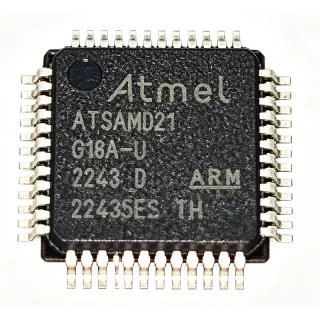
ATSAMD21G18A-AF - 48MHz Cortex-M0+ MCU 256KB Flash | Microchip
MPN: ATSAMD21G18A-AF ✓ Hoạt độngATSAMD21G18A-AF Tóm tắt
What is a Cortex-M0+ microcontroller? A Cortex-M0+ microcontroller is an ARM-based 32-bit processor core designed for energy-efficient embedded computing. It belongs to the Cortex-M family of microcontrollers, which sit within the broader category of microcontrollers and, at the top level, integrated circuits. The Cortex-M0+ uses a 2-stage pipeline with a Thumb/Thumb-2 instruction subset, delivers deterministic interrupt response, and offers significantly higher DMIPS/mW than 8-bit AVR or 8051 alternatives, making it ideal for battery-powered IoT nodes and portable consumer products.
Key features of the ATSAMD21G18A-AF include a full-speed USB 2.0 device with on-the-go (OTG) support, a 12-bit 350 ksps ADC, a 10-bit 350 ksps DAC, up to six SERCOM channels, and up to five 16-bit Timer/Counters. The device also integrates a 12-channel DMA controller, a 12-channel Event System, and two-pin Serial Wire Debug (SWD) for programming and boundary-scan. It supports SleepWalking peripherals, idle and standby sleep modes, and is pin-compatible with the SAM D20 family for simple migration.
The ATSAMD21G18A-AF uses a single 1.62V to 3.63V supply rail and offers multiple low-power modes that drop quiescent current to a few microamps in standby. The integrated full-speed USB PHY eliminates the need for an external transceiver, simplifying USB-enabled designs. The peripheral Event System and DMAC allow data movement without CPU intervention, enabling deterministic response and freeing the core for application logic.
Typical applications include smart-home sensor hubs, IoT edge nodes, industrial HMI panels, low-power wireless sensor platforms, and battery-powered consumer devices such as fitness wearables. The device is also widely used in maker and education platforms, including Arduino-compatible boards that leverage its native USB, capacitive touch, and PWM peripherals.
When designing with the ATSAMD21G18A-AF, ensure the VDD decoupling network includes a 100 nF capacitor close to each supply pin and a bulk 4.7 uF capacitor to handle USB inrush current. Plan the boot loader pin (BOOTPROT) configuration early if field firmware updates are required, and reserve a dedicated SWD header for in-circuit debugging.
This page synthesizes distributor pricing, drop-in alternatives, and practical design notes not found in the manufacturer datasheet alone.
Bộ thay thế dễ dàng lắp đặt cho ATSAMD21G18A-AF — cùng gói, chân-to-chân tương thích. Các bộ phận yêu cầu hàn PCB bị loại trừ.
Các biến thể trong loạt này
Các mẫu cùng loạt có thể lắp đặt dễ dàng tương thích với ATSAMD21G18A-AF (cùng hình factor và footprint) — khác nhau ở ADC, Operating Temperature, Package, USB, RoHS Status.
ATSAMD21G18A-AFT
✅ Drop-InLiên hệ để biết giá
Xem tài liệu →ATSAMD21G18A-AU
✅ Drop-In✗ Hết hàng
$2.78 / Đơn vị
Xem tài liệu →ATSAMD21G18A-AUT
✅ Drop-In📋 Tham chiếu thay thế (không có trong danh mục)
ATSAMD21G17A-AF
✅ Drop-InLiên hệ để biết giá
Xem tài liệu →ATSAMD21G17A-AFT
✅ Drop-InLiên hệ để biết giá
Xem tài liệu →ATSAMD21G18A-MUT
✅ Drop-In ⚠️ Thông số chưa được xác minhLiên hệ để biết giá
Xem tài liệu →ATSAMD21G18A-AF Tỷ lệ tối đa & tính chất điện
| Core | ARM Cortex-M0+ (SAM D21) |
| Core Architecture | 32-bit RISC, Thumb/Thumb-2 instruction set |
| Maximum CPU Clock | 48 MHz |
| Flash Memory | 256 KB |
| SRAM | 32 KB |
| Supply Voltage (VDD) | 1.62 V to 3.63 V |
| Hộp | 48-pin TQFP (7x7 mm) |
| Kiểu lắp đặt | Surface Mount |
| ADC | 12-bit, up to 350 ksps |
| DAC | 10-bit, 350 ksps |
| USB | Full-speed USB 2.0 device with on-the-go (OTG) |
| SERCOM Channels | Up to 6 (configurable as I2C/SPI/UART) |
| Timers | Up to 5 x 16-bit Timer/Counters (TC) |
| DMA Channels | 12-channel DMAC |
| Event System | 12-channel inter-peripheral |
| Debug Interface | Two-pin Serial Wire Debug (SWD) |
| Nhiệt độ hoạt động | -40C to +85C |
| Trạng thái RoHS | Compliant |
Cấu hình chân ATSAMD21G18A-AF
| Chân 1 | PA00 — GPIO / XIN32 (external 32 kHz crystal input) |
| Chân 2 | PA01 — GPIO / XOUT32 (external 32 kHz crystal output) |
| Chân 3 | PA02 — GPIO / AIN0 (ADC input) |
| Chân 4 | PA03 — GPIO / AIN1 (ADC input) / VREFA reference voltage |
| Chân 5 | GND — Ground |
| Chân 6 | VDD — Digital supply voltage 1.62 V to 3.63 V |
| Chân 7 | PA04 — GPIO / AIN2 / VREFB |
| Chân 8 | PA05 — GPIO / AIN3 |
| Chân 9 | PA06 — GPIO / AIN4 |
| Chân 10 | PA07 — GPIO / AIN5 |
| Chân 11 | PA08 — GPIO / AIN6 / SERCOM0 PAD0 / I2S SD0 |
| Chân 12 | PA09 — GPIO / AIN7 / SERCOM0 PAD1 / I2S MCK0 |
| Chân 13 | PA10 — GPIO / AIN8 / SERCOM0 PAD2 / I2S SCK0 |
| Chân 14 | PA11 — GPIO / AIN9 / SERCOM0 PAD3 / I2S FS0 |
| Chân 15 | VDD — Digital supply voltage |
| Chân 16 | GND — Ground |
| Chân 17 | PA12 — GPIO / SERCOM2 PAD0 / USB D- |
| Chân 18 | PA13 — GPIO / SERCOM2 PAD1 / USB D+ |
| Chân 19 | PA14 — GPIO / SERCOM2 PAD2 / XIN (main crystal input) |
| Chân 20 | PA15 — GPIO / SERCOM2 PAD3 / XOUT (main crystal output) |
| Chân 21 | PA16 — GPIO / SERCOM1 PAD0 / I2S SD1 |
| Chân 22 | PA17 — GPIO / SERCOM1 PAD1 / I2S MCK1 |
| Chân 23 | PA18 — GPIO / SERCOM1 PAD2 / I2S SCK1 |
| Chân 24 | PA19 — GPIO / SERCOM1 PAD3 / I2S FS1 |
| Chân 25 | PA20 — GPIO / SERCOM5 PAD2 / TCC0 channel 6 |
| Chân 26 | PA21 — GPIO / SERCOM5 PAD3 / TCC0 channel 7 |
| Chân 27 | PA22 — GPIO / SERCOM3 PAD0 / TCC1 channel 4 |
| Chân 28 | PA23 — GPIO / SERCOM3 PAD1 / TCC1 channel 5 |
| Chân 29 | PA24 — GPIO / SERCOM3 PAD2 / USB ID |
| Chân 30 | PA25 — GPIO / SERCOM3 PAD3 / USB VBUS detect |
| Chân 31 | GND — Ground |
| Chân 32 | VDD — Digital supply voltage |
| Chân 33 | PA26 — GPIO / DAC0 output |
| Chân 34 | PA27 — GPIO / DAC1 output |
| Chân 35 | PA28 — GPIO / RESETN (external reset, active low) |
| Chân 36 | PA29 — GPIO / SWDIO (Serial Wire Debug data) |
| Chân 37 | PA30 — GPIO / SWCLK (Serial Wire Debug clock) |
| Chân 38 | PA31 — GPIO / BOOTPROT / SERCOM5 PAD1 |
| Chân 39 | PB00 — GPIO / SERCOM5 PAD2 |
| Chân 40 | PB01 — GPIO / SERCOM5 PAD3 |
| Chân 41 | PB02 — GPIO / SERCOM5 PAD0 / TCC0 channel 0 |
| Chân 42 | PB03 — GPIO / SERCOM5 PAD1 / TCC0 channel 1 |
| Chân 43 | PB04 — GPIO / SERCOM3 PAD0 |
| Chân 44 | PB05 — GPIO / SERCOM3 PAD1 |
| Chân 45 | PB06 — GPIO / SERCOM3 PAD2 |
| Chân 46 | PB07 — GPIO / SERCOM3 PAD3 |
| Chân 47 | PB08 — GPIO / SERCOM4 PAD0 / TCC1 channel 0 |
| Chân 48 | PB09 — GPIO / SERCOM4 PAD1 / TCC1 channel 1 |
Ứng dụng tiêu biểu
ATSAMD21G18A-AF phù hợp cho 6 Áp dụngs: Smart Home Sensor Hubs, USB HID Devices and Wearables, Industrial Sensor Front-Ends, Low-Power Wireless IoT Nodes, Battery-Powered Metering, Consumer HMI and Maker Platforms.
Smart Home Sensor Hubs
The ATSAMD21G18A-AF's 256 KB Flash holds Zigbee or Thread application stacks plus room for application logic, while its six SERCOM channels let the same MCU drive multiple I2C sensors, an SPI display, and a UART radio concurrently. The 48 MHz Cortex-M0+ runs sensor-fusion loops comfortably and the 12-bit ADC at 350 ksps supports simultaneous temperature, humidity, and light sampling. Dropping into standby between events drops quiescent current to single-digit microamps, suiting coin-cell and energy-harvesting deployments.
Được đề xuất
USB HID Devices and Wearables
Integrated full-speed USB 2.0 with on-the-go support removes the need for an external PHY, making the ATSAMD21G18A-AF ideal for USB HID peripherals such as keyboards, mice, audio interfaces, and MIDI controllers. The 48-pin TQFP gives designers 38 GPIO pins for capacitive touch or rotary encoder matrices, and the 10-bit DAC at 350 ksps can drive simple audio cue tones. SleepWalking peripherals let the device wake on USB activity without CPU intervention, preserving battery life in portable accessories.
Được đề xuất
Industrial Sensor Front-Ends
In industrial 4-20 mA loop-powered transmitters and machine-vibration monitors, the ATSAMD21G18A-AF delivers the deterministic response of a Cortex-M0+ while consuming under 10 uA in standby. The 12-bit ADC and the integrated op-amp support ratiometric RTD and strain-gauge measurement, while the Event System guarantees that timing-critical interrupts are never blocked by DMA transfers. The wide 1.62 V to 3.63 V supply range tolerates noisy 24 V-derived rails after regulation.
Được đề xuất
Low-Power Wireless IoT Nodes
For battery-powered LoRa, BLE, or sub-GHz sensor nodes, the ATSAMD21G18A-AF pairs with modules such as the RN2483 or nRF52832 over UART or SPI. The 256 KB Flash is enough to hold LoRaWAN stacks and user application firmware concurrently, while the 32 KB SRAM buffers radio packet payloads. Standby current around 2-5 uA allows multi-year operation from a pair of AA cells when wake-up duty cycles are kept low.
Được đề xuất
Battery-Powered Metering
Utility meters for water, gas, and electricity benefit from the ATSAMD21G18A-AF's combination of precise 12-bit ADC channels, low standby current, and the integrated RTC plus sleep modes. The Event System can trigger ADC conversions from timer events without waking the CPU, enabling tamper detection and pulse counting at single-digit microamp currents. The 48-pin TQFP leaves enough GPIO to drive e-paper or segmented LCD interfaces through inexpensive external drivers.
Được đề xuất
Consumer HMI and Maker Platforms
Arduino-compatible boards such as the Adafruit Feather M0 and the Arduino Zero use the ATSAMD21G18A-AF because its native USB, capacitive touch I/O, and PWM peripherals cover the full maker-feature list. The 48 MHz core drives small TFT displays over SPI, the 10-bit DAC generates simple audio cues, and the SWD interface lets students debug firmware using free MPLAB X tools. The 256 KB Flash comfortably hosts CircuitPython and Arduino libraries.
Được đề xuất
Tóm tắt các sản phẩm được đề xuất
Dữ liệu tham khảo kỹ thuật cho ATSAMD21G18A-AF — so sánh, hướng dẫn thiết kế và thông tin tuân thủ.
Hướng dẫn chọn lựa
So sánh với các sản phẩm thay thế
| Tham số | Sản phẩm này | ATSAMD21G18A-AFT | ATSAMD21G18A-AU | ATSAMD21G18A-AUT | ATSAMD21G17A-AF | ATSAMD21G17A-AFT | ATSAMD21G18A-MUT |
|---|---|---|---|---|---|---|---|
| Brand | Microchip Technology | Microchip Technology | Microchip Technology | Microchip Technology | Microchip Technology | Microchip Technology | Microchip Technology |
| Package | 48-pin TQFP (7x7 mm) | 48-pin TQFP (7x7 mm) | 48-pin TQFP (7x7 mm) | 48-pin TQFP (7x7 mm) | 48-pin TQFP (7x7 mm) | 48-pin TQFP (7x7 mm) | 48-pin QFN (7x7 mm) |
| Core | ARM Cortex-M0+ | ARM Cortex-M0+ | ARM Cortex-M0+ | ARM Cortex-M0+ | ARM Cortex-M0+ | ARM Cortex-M0+ | ARM Cortex-M0+ |
| Max CPU Clock | 48 MHz | 48 MHz | 48 MHz | 48 MHz | 48 MHz | 48 MHz | 48 MHz |
| Flash Memory | 256 KB | 256 KB | 256 KB | 256 KB | 128 KB | 128 KB | 256 KB |
| SRAM | 32 KB | 32 KB | 32 KB | 32 KB | 32 KB | 32 KB | 32 KB |
| USB Support | USB 2.0 FS with OTG | USB 2.0 FS with OTG | USB 2.0 FS with OTG | USB 2.0 FS with OTG | USB 2.0 FS with OTG | USB 2.0 FS with OTG | USB 2.0 FS with OTG |
| Operating Temperature | -40C to +85C | -40C to +85C | -40C to +85C | -40C to +85C | -40C to +85C | -40C to +85C | -40C to +85C |
Bảo phân biệt quan trọng
- Native full-speed USB 2.0 with OTG integrated (vsATSAMD20G18A-AU)
- Larger Flash in the same TQFP-48 package (vsATSAMD21G17A-AF)
- TQFP-48 footprint eases hand soldering vs QFN (vsATSAMD21G18A-MUT)
Ghi chú thiết kế
Place a 100 nF decoupling capacitor within 3 mm of every VDD pin (pins 6, 15, 32) and a bulk 4.7 uF capacitor near the regulator output to handle USB inrush current. The SAM D21 internal regulator derives the USB 3.3 V from VDDIN, so VDDIN must be at least 3.0 V whenever the USB transceiver is enabled.
Route the two SWD pins (SWDIO on PA29, SWCLK on PA30) away from switching signals and provide a dedicated 2x5 or 1x6 header for in-circuit programming. If using the external main crystal on PA14/PA15, keep the traces short, symmetrical, and guarded by a ground plane; failure to do so can corrupt the high-speed USB reference clock.
Do not leave the BOOTPROT pin (PA31) floating in production firmware; tie it through a 10 kOhm resistor to VDD or GND per the bootloader configuration to avoid accidental bootloader entry. The 32 kHz crystal pins (PA00/PA01) must use a crystal with load capacitance matched to the on-chip load configuration, or RTC accuracy will suffer.
When using the integrated USB peripheral, the D-/D+ pair (PA12/PA13) must be routed as a 90 ohm differential pair on the top layer with no splits and an uninterrupted ground reference beneath. Place the USB connector's shield-decoupling capacitor within 10 mm of the connector shell to ensure EMI compliance.
Thông tin tuân thủ
RoHS and REACH compliance stated on the Microchip product page. Not AEC-Q100 qualified; consider ATSAMx automotive variants for automotive deployments.