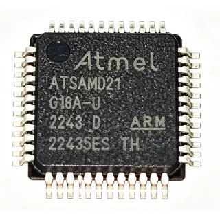
DSPIC33FJ06GS001-I/P - 16-bit 40 MIPS DSC 6KB | Microchip
MPN: DSPIC33FJ06GS001-I/P ✓ Hoạt độngDSPIC33FJ06GS001-I/P Tóm tắt
A digital signal controller combines the computational capability of a DSP core with the peripherals and ease of use of a microcontroller. Within the power-management hierarchy, a DSC sits between a general-purpose MCU and a dedicated DSP: it executes fast multiply-accumulate instructions for control loops while retaining GPIO, timers, and serial interfaces. The dsPIC33F family from Microchip is a widely adopted 16-bit DSC platform for embedded digital power and motor control.
Key features of this GS-series part include a high-speed PWM module purpose-built for switched-mode power supplies (SMPS), analog comparators, a 10-bit ADC with simultaneous multi-channel sampling support, and connectivity via I2C, SPI, UART/USART, IrDA, and LIN. Peripherals such as brown-out detect/reset and power-on reset improve system robustness.
Architecturally, the dsPIC33F core uses a 24-bit instruction word with a modified Harvard bus, achieving single-cycle MAC execution that sustains deterministic control-loop timing at 40 MIPS. Multiple PGECx/PGEDx pin pairs support In-Circuit Serial Programming (ICSP) and debugging with standard Microchip tools.
Typical applications include digital power supplies, interleaved power factor correction (PFC) converters, battery chargers, LED drivers, and lighting ballasts, where the high-resolution PWM directly drives half-bridge or flyback power stages.
For design, decouple both VDD pins with 0.1 uF ceramics close to the package, use any matched PGEC/PGED pair consistently for ICSP, and budget flash carefully since 6 KB suits compact control firmware only.
This page synthesizes distributor pricing, drop-in alternatives, pinout data, and practical design notes not found in the manufacturer datasheet, as of 2026-09-26.
Bộ thay thế dễ dàng lắp đặt cho DSPIC33FJ06GS001-I/P — cùng gói, chân-to-chân tương thích. Các bộ phận yêu cầu hàn PCB bị loại trừ.
Các biến thể trong loạt này
Các mẫu cùng loạt có thể lắp đặt dễ dàng tương thích với DSPIC33FJ06GS001-I/P (cùng hình factor và footprint) — khác nhau ở Operating Temperature, PWM Module, Supply Voltage, Package, ADC.
DSPIC33FJ06GS001-E/P
✅ Drop-InLiên hệ để biết giá
Xem tài liệu →DSPIC33FJ06GS101A-I/P
✅ Drop-In ⚠️ Thông số chưa được xác minhLiên hệ để biết giá
Xem tài liệu →DSPIC33FJ06GS001-I/P Tỷ lệ tối đa & tính chất điện
| Core | dsPIC33F 16-bit |
| Max Speed | 40 MIPS |
| Program Memory (Flash) | 6 KB (2K x 24) |
| RAM | 256 bytes |
| Điện áp cung cấp | 3.3 V |
| Hộp | 18-PDIP (0.300 in, 7.62 mm) |
| Nhiệt độ hoạt động | -40C to +85C |
| Connectivity | I2C, SPI, UART/USART, IrDA, LIN |
| Peripherals | Brown-out Detect/Reset, POR, High-Speed PWM, Comparators, ADC |
| PWM Module | High-Speed PWM for SMPS |
| Timers | 4 |
| External Interrupts | 3 |
| Instruction Word Width | 24-bit |
| Programming Interface | ICSP via PGECx/PGEDx pairs |
| Kiểu lắp đặt | Through Hole |
| Packaging | Tube |
| Product Status | In Production (per Microchip product page) |
Cấu hình chân DSPIC33FJ06GS001-I/P
| Chân 1 | MCLR — Master clear reset / programming voltage input |
| Chân 2 | AN0 — Analog input 0 / comparator input / GPIO |
| Chân 3 | AN1 — Analog input 1 / comparator input / GPIO |
| Chân 4 | AN2 — Analog input 2 / comparator input / GPIO |
| Chân 5 | AN3 — Analog input 3 / GPIO |
| Chân 6 | PGED1 — ICSP data pin pair 1 / GPIO |
| Chân 7 | PGEC1 — ICSP clock pin pair 1 / GPIO |
| Chân 8 | PWM1L — High-speed PWM channel 1 low output |
| Chân 9 | PWM1H — High-speed PWM channel 1 high output |
| Chân 10 | VSS — Ground reference |
| Chân 11 | VDD — Positive supply, 3.3 V |
| Chân 12 | PWM2L — High-speed PWM channel 2 low output |
| Chân 13 | PWM2H — High-speed PWM channel 2 high output |
| Chân 14 | PGED2 — ICSP data pin pair 2 / GPIO |
| Chân 15 | PGEC2 — ICSP clock pin pair 2 / GPIO |
| Chân 16 | RP1 — Remappable peripheral pin 1 (UART/SPI/I2C etc.) |
| Chân 17 | RP2 — Remappable peripheral pin 2 (UART/SPI/I2C etc.) |
| Chân 18 | RP3 — Remappable peripheral pin 3 (UART/SPI/I2C etc.) |
Ứng dụng tiêu biểu
DSPIC33FJ06GS001-I/P phù hợp cho 6 Áp dụngs: Digital Power Supplies (SMPS), Power Factor Correction (PFC), Battery Chargers, LED Drivers and Lighting Ballasts, Embedded Industrial Control, Prototyping and Education.
Digital Power Supplies (SMPS)
The DSPIC33FJ06GS001-I/P is purpose-built for switched-mode power supply control: its high-speed PWM module generates complementary outputs with hardware dead-time insertion, while onboard comparators provide cycle-by-cycle overcurrent protection with nanosecond-class response. The 40 MIPS dsPIC33F core closes voltage and current loops using single-cycle MAC instructions, sustaining deterministic control at switching frequencies typical of flyback and forward converters. Programmed with 6 KB of flash and running from a 3.3V rail, it replaces analog control ICs while adding programmability, digital compensation, and telemetry via UART or I2C. Place it on the secondary or primary controller site with ADC inputs on the feedback dividers; the trade-off versus a pure analog PWM controller is firmware complexity, in exchange for adaptive, tunable loop behavior.
Được đề xuất
Power Factor Correction (PFC)
Microchip's interleaved PFC reference design for SMPS dsPIC controllers demonstrates this family driving universal-input PFC stages producing a single high-voltage DC output up to 350 W. The DSPIC33FJ06GS001-I/P executes average-current-mode PFC control: the ADC samples input voltage, inductor current, and bus voltage, while the high-speed PWM updates duty cycle every switching cycle at 40 MIPS without software jitter. On-chip comparators back up the digital loop with hardware current limiting. The 3.3V controller supervises the boost stage, manages soft-start and brown-out behavior using its POR and brown-out reset peripherals, and reports status over UART or LIN. Digital PFC enables adaptive gain scheduling across the universal input range - impossible with fixed analog compensation networks.
Được đề xuất
Battery Chargers
For smart battery chargers, the DSPIC33FJ06GS001-I/P combines the control elements a charging algorithm needs in one 18-pin through-hole device: high-resolution PWM drives the buck or flyback power stage, the 10-bit ADC measures battery voltage and current for CC/CV profiling, and comparators implement fast hardware overcurrent trips independent of firmware latency. The 40 MIPS core runs temperature-compensated charge curves, termination detection, and fault state machines within the 6 KB flash budget. Its I2C interface reads battery-pack smart fuel-gauge ICs, while UART supports host reporting. Operating from -40C to +85C in industrial-grade silicon, the -I/P suits charger enclosures without forced airflow, and its through-hole PDIP package simplifies prototyping and low-volume production.
Được đề xuất
LED Drivers and Lighting Ballasts
Digital LED drivers benefit from the DSPIC33FJ06GS001-I/P's precise PWM granularity and dimming control. The high-speed PWM module produces phase-shifted or complementary outputs with programmable dead time, enabling buck, boost, or SEPIC LED drivers with accurate current regulation. The ADC samples the LED current sense resistor each cycle, and the 40 MIPS loop maintains constant current despite forward-voltage variation and temperature drift. Onboard comparators provide instantaneous short-circuit protection for the LED string. Dimming curves (triac-phase, 0-10V via ADC, or PWM input) are implemented in firmware, and I2C or UART links the driver to lighting network controllers. The 3.3V, 6 KB flash controller fits cost-sensitive luminaire electronics with industrial temperature margins.
Được đề xuất
Embedded Industrial Control
Beyond power conversion, the DSPIC33FJ06GS001-I/P serves as a compact 16-bit embedded controller where deterministic execution matters: sensor signal conditioning, relay and actuator sequencing, and small motion loops. Its four timers, three external interrupt sources, and remappable I/O pins accommodate mixed signal-timing tasks, while I2C, SPI, and UART cover inter-chip communication with displays, memory, and supervisory PLCs. LIN and IrDA support extend connectivity into automotive-adjacent and legacy serial systems. The through-hole 18-pin PDIP package is a practical advantage for industrial maintenance boards, retrofit controllers, and educational platforms where hand soldering and socketed replacement are valued. Brown-out reset and power-on reset peripherals guarantee predictable startup across noisy factory power environments.
Được đề xuất
Prototyping and Education
The PDIP through-hole package of the DSPIC33FJ06GS001-I/P makes it an excellent vehicle for learning 16-bit embedded DSP programming and digital power electronics. It inserts directly into breadboards and perforated boards, and programs via ICSP using any PGECx/PGEDx pair with common tools such as PICkit or NSDSP programmers, all supported in MPLAB X with free compiler options. Students can implement SMPS loops, ADC sampling, and UART communication on a genuinely industrial-grade part rather than a stripped-down evaluation MCU. XAIPART pricing as of 2026-09-26 starts around $4.62 at quantity 1, keeping lab budgets low, and tube packaging suits university stockrooms. The same silicon scales into the wider dsPIC33F family for coursework progression.
Được đề xuất
Tóm tắt các sản phẩm được đề xuất
Dữ liệu tham khảo kỹ thuật cho DSPIC33FJ06GS001-I/P — so sánh, hướng dẫn thiết kế và thông tin tuân thủ.
Hướng dẫn chọn lựa
So sánh với các sản phẩm thay thế
| Tham số | Sản phẩm này | DSPIC33FJ06GS001-E/P | DSPIC33FJ06GS101A-I/P |
|---|---|---|---|
| Package | 18-PDIP (0.300 in, 7.62 mm) | 18-PDIP (0.300 in) - same | 18-PDIP (0.300 in) - same |
| Brand | Microchip Technology | Microchip Technology | Microchip Technology |
| Max Speed | 40 MIPS | 40 MIPS | 40 MIPS |
| Operating Temperature | -40C to +85C | -40C to +125C | -40C to +85C |
| Supply Voltage | 3.3 V | 3.3 V | 3.3 V |
| High-Speed SMPS PWM | Yes | Yes | Yes |
Bảo phân biệt quan trọng
- Standard industrial temperature range at lower cost (vsDSPIC33FJ06GS001-E/P)
- Mature first-revision silicon for firmware continuity (vsDSPIC33FJ06GS101A-I/P)
- Honest limitation: minimal memory margin (vsDSPIC33FJ06GS001-E/P)
Ghi chú thiết kế
Decouple VDD with a 0.1 uF ceramic capacitor placed within 5 mm of the VDD pin, plus a 4.7-10 uF bulk capacitor near the controller. In SMPS layouts, keep the DSC's analog ground reference separate from the power-stage gate-drive return until a single-point star connection; switching-node ringing on ANx inputs corrupts ADC readings. Connect all VSS pins solidly to the ground plane.
ICSP requires a matched PGECx/PGEDx pair: if ICSPCLK uses PGEC2, ICSPDAT must use PGED2 - mixing pairs from different pairs prevents programming. Do not load PGECx/PGEDx pins with LEDs or pull-downs above Microchip's recommended limits, or programming reliability suffers. Budget flash carefully: 6 KB (2K instructions) fits a compact SMPS control loop but leaves little room for protocol stacks.
Estimated: at 40 MIPS typical active current in the tens-of-mA class on a 3.3V rail, dissipation is on the order of 0.1 W - negligible for the 18-PDIP package even in sealed enclosures up to +85C ambient. Verify against the datasheet current-consumption tables for your exact clock configuration (FRC vs crystal, PLL settings) if enclosure thermal margins are tight.
Thông tin tuân thủ
Compliance details were not present in the provided web data; verify on the Microchip product page before export documentation.