LPC11U68JBD48K - 50MHz Cortex-M0+ MCU | NXP | USB
MPN: LPC11U68JBD48K ✓ Hoạt độngLPC11U68JBD48K Tóm tắt
A microcontroller is a programmable semiconductor that integrates a processor core, memory, and peripherals into one component. The LPC11U68 belongs to NXP's LPC11Uxx family, a low-cost family based on Arm Cortex-M0+ and Cortex-M0 cores. This MCU family targets control and embedded applications that need 32-bit processing, compact code size, low power consumption, and deterministic peripheral operation without the cost and complexity of a higher-performance processor.
The LPC11U68JBD48K combines a 50 MHz Cortex-M0+ core with 256 KB of on-chip flash and 36 KB of SRAM. Its 4 KB EEPROM provides nonvolatile storage for parameters, calibration values, or configuration data. USB support makes the device suitable for USB-connected peripherals, while the 12-bit ADC supports analog measurement from sensors, potentiometers, and resistive divider networks. The extended -40 °C to +105 °C temperature range also permits operation across industrial temperature environments.
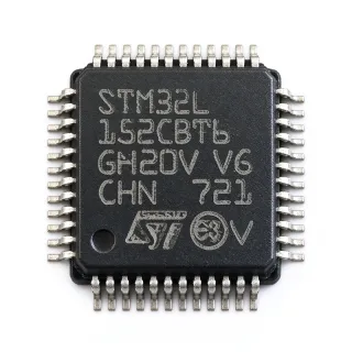
The 48-LQFP package provides a practical option for through-hole assembly and prototype development because its leads are inspectable and accessible on a conventional PCB. Its 7 mm by 7 mm body is larger than the smallest microcontroller packages, but it simplifies hand soldering, signal probing, and rework. Board planners must preserve the manufacturer's land pattern and observe the specified pin, clearance, and soldering requirements.
Typical uses include industrial control modules, USB-to-serial or USB-connected data-acquisition equipment, compact sensor interfaces, building-control nodes, and low-cost embedded products. In an analog measurement design, the 12-bit ADC can acquire sensor signals while the Cortex-M0+ core performs filtering, calibration, and data packaging. In a USB peripheral, the integrated USB interface can reduce external connectivity requirements while the MCU manages the application protocol.
Design consideration: verify the operating voltage, peripheral pin multiplexing, USB electrical requirements, clock configuration, and programming interface against the manufacturer datasheet before finalizing the PCB. Use the specified decoupling and programming-interface layout, and account for every alternate-function pin used by the application.
This page consolidates the manufacturer specifications, commercial inquiry workflow, package information, application guidance, and cross-reference status for LPC11U68JBD48K into one engineering-focused reference.
Bộ thay thế dễ dàng lắp đặt cho LPC11U68JBD48K — cùng gói, chân-to-chân tương thích. Các bộ phận yêu cầu hàn PCB bị loại trừ.
Các biến thể trong loạt này
Các mẫu cùng loạt có thể lắp đặt dễ dàng tương thích với LPC11U68JBD48K (cùng hình factor và footprint) — khác nhau ở Package, Product Type.
Không có bộ thay thế dễ dàng lắp đặt sẵn có cho sản phẩm này.
Yêu cầu các bộ thay thếLPC11U68JBD48K Tỷ lệ tối đa & tính chất điện
| Product Type | 32-bit microcontroller IC |
| Processor Core | Arm Cortex-M0+ |
| Maximum CPU Frequency | 50 MHz |
| Flash Memory | 256 KB |
| Flash Organization | 256K x 8 bits |
| SRAM | 36 KB |
| EEPROM | 4 KB |
| ADC Resolution | 12 bits |
| USB Connectivity | USB |
| Operating Voltage | 3.3 V |
| Minimum Operating Temperature | -40 °C |
| Maximum Operating Temperature | +105 °C |
| Hộp | 48-pin LQFP, 7 mm x 7 mm |
| Kiểu lắp đặt | Surface mount |
| Architecture | 32-bit RISC |
Hướng dẫn cấu hình chân LPC11U68JBD48K 48-pin lqfp, 7 mm x 7 mm
Cấu hình chân cho LPC11U68JBD48K (48-pin lqfp, 7 mm x 7 mm gói). IC số này bao gồm chân GPIO, giao diện truyền thông (UART, SPI, I2C) và chân nguồn. Tham khảo tài liệu thông số kỹ thuật của nhà sản xuất để biết các chức năng chân thay thế và tùy chọn cấu hình. Cực kỳ quan trọng cho thiết kế hệ thống tích hợp và lập trình PCB.

Không có dữ liệu chân cụ thể sẵn có cho LPC11U68JBD48K.
Tham khảo: tài liệu kỹ thuật cho cấu hình chân đầy đủ.
Ứng dụng tiêu biểu
LPC11U68JBD48K phù hợp cho 6 Áp dụngs: USB Connected Sensor Interface, Industrial Control Module, USB Data Acquisition Unit, Building Control Node, Programmable Logic Controller, Portable Measurement Instrument.
USB Connected Sensor Interface
The LPC11U68JBD48K fits a USB-connected sensing node because its 50 MHz Arm Cortex-M0+ core can acquire and process data while USB provides a direct host interface. The 12-bit ADC can serve resistive dividers, thermistors, potentiometers, and other analog sensors whose signals fall within the device's input limits. The 256 KB of flash stores firmware and calibration tables, while 36 KB of SRAM supports buffering, filtering, and protocol handling. Designers should verify the ADC acquisition characteristics, USB transceiver requirements, clock setup, and regulator sequencing in the manufacturer datasheet.
Industrial Control Module
The LPC11U68JBD48K is suitable for compact industrial control modules that combine digital I/O, analog measurement, and a communications link. Its 50 MHz Cortex-M0+ core provides more processing capability than a basic 8-bit controller, while 256 KB of flash and 36 KB of SRAM allow the firmware to combine control logic, diagnostics, and communication buffers. The -40 °C to +105 °C rating supports extended ambient conditions. Industrial implementations still need appropriate input protection, isolation where required, grounding, and safety testing at the complete-system level.
USB Data Acquisition Unit
For a compact USB data-acquisition unit, the LPC11U68JBD48K can use its 12-bit ADC for analog measurements and its 50 MHz Cortex-M0+ core for filtering, scaling, timestamping, and packet preparation. USB connectivity avoids requiring a separate communications controller for a basic peripheral design, while 4 KB of EEPROM can retain calibration constants or device settings. The 48-LQFP package is also convenient for hand assembly and probing. Confirm input impedance, sample-and-hold behavior, ADC noise, USB clocking, and data-packet timing against the manufacturer documentation.
Building Control Node
The LPC11U68JBD48K can serve as the central controller in a low-cost building-control node that monitors sensors and operates actuators through digital and analog interfaces. Its 256 KB flash accommodates application firmware and configuration logic, while the 4 KB EEPROM can preserve node settings across power cycles. The -40 °C to +105 °C operating range suits many indoor and industrial enclosure environments. A production design must add appropriate transient protection for connected field wiring and validate communication reliability under electrically noisy conditions.
Programmable Logic Controller
The LPC11U68JBD48K can be used in a small programmable logic controller when designers need more timing precision and code capacity than a basic 8-bit MCU provides. The 50 MHz Cortex-M0+ core supports deterministic task execution, while the configurable peripheral family can reduce the need for external logic. Its 48-LQFP format makes the device practical for boards assembled with conventional leaded-package tooling. Before selecting it, map every required PLC signal to the available port pins and confirm timer, serial, ADC, and interrupt resources in the pin table.
Portable Measurement Instrument
The LPC11U68JBD48K supports portable measurement instruments that combine analog sensing, local processing, and USB connectivity. The 12-bit ADC provides a practical measurement resolution for many non-precision applications, while the Cortex-M0+ core can apply calibration and filtering without offloading all processing to a host. With 36 KB of SRAM, the MCU can buffer samples, and with 256 KB of flash it can store firmware, configuration, and calibration tables. The -40 °C to +105 °C range aids product design across demanding ambient environments, subject to battery and display requirements.
Dữ liệu tham khảo kỹ thuật cho LPC11U68JBD48K — so sánh, hướng dẫn thiết kế và thông tin tuân thủ.
Hướng dẫn chọn lựa
An STM32F103 variant should be considered only as a redesign candidate because pin assignment, USB implementation, peripheral resources, and board layout may differ. PIC24 and ATtiny alternatives can serve simpler control tasks, but they do not match the target's combination of CPU performance, memory, USB, and ADC resolution. A no-software-change substitution is not established, so verify the complete pin table, electrical limits, peripheral mapping, and programming process before changing the released MPN.
So sánh với các sản phẩm thay thế
| Tham số | Sản phẩm này |
|---|---|
| Brand | NXP Semiconductors |
| Package | 48-pin LQFP, 7 mm x 7 mm |
| Processor Core | Arm Cortex-M0+ |
| Maximum CPU Frequency | 50 MHz |
| Flash Memory | 256 KB |
| SRAM | 36 KB |
| EEPROM | 4 KB |
| ADC Resolution | 12 bits |
| Connectivity | USB |
| Operating Voltage | 3.3 V |
| Operating Temperature | -40 °C to +105 °C |
Bảo phân biệt quan trọng
- Integrated memory and persistent configuration (vsSTM32F103C8T6)
- USB-enabled compact controller (vsPIC24F16KL402-E/MQ)
- Extended temperature operation (vsATtiny88-AUR)
Ghi chú thiết kế
Use the NXP manufacturer land pattern for the 48-LQFP, 7 mm by 7 mm package and preserve its pin numbering orientation. Place decoupling capacitors beside the relevant supply pins with short ground returns, and avoid routing high-speed or high-current USB signals across the ADC input area. Confirm courtyard clearance against adjacent components and provide access to the programming interface. Because alternate functions are multiplexed, complete the pin assignment before finalizing routing and component placement.
Route USB D+ and D- as a controlled-impedance, tightly coupled pair with a continuous reference plane and minimal stubs. Keep the pair away from ADC inputs, switching-regulator inductors, crystal circuitry, and long parallel runs that can increase coupling. Follow the device's USB clock, capacitor, and series-resistor recommendations in the manufacturer datasheet. If the board exceeds a simple direct connection, evaluate ESD protection, common-mode choke, or series-impedance choices that do not compromise signal integrity.
Do not assume that a 12-bit ADC automatically provides accurate measurements. Establish the sensor's full-scale range, select the correct input channel, configure the acquisition time, and allow analog settling before sampling. Use the ADC reference and supply arrangement specified by NXP, and treat digital activity near analog inputs as a potential error source. Firmware should also apply calibration, filtering, saturation detection, and fault reporting rather than forwarding unprocessed conversion results.
Design the 3.3 V supply with the startup, sequencing, current, and decoupling requirements specified in the manufacturer datasheet. Verify the voltage tolerance at every power pin under maximum CPU activity, USB load, and peripheral usage. If a system rail is generated by a switching converter, reserve filtering and test points for sensitive analog measurements. Do not use nominal rail voltage as a substitute for checking minimum and maximum operating conditions across temperature.
Thông tin tuân thủ
No specific RoHS, REACH, AEC-Q100, lead-free, halogen-free, or conflict-minerals declaration was identified for the exact ordering code.