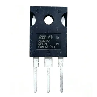
STW30N60M2 - 600V 30A N-Channel Power MOSFET | STMicroelectronics
MPN: STW30N60M2 ✓ Hoạt độngSTW30N60M2 Tóm tắt
A power MOSFET is a type of field-effect transistor designed to handle significant power levels in switching and amplification circuits. It operates by controlling the flow of current through a semiconductor channel using an electric field, offering high switching speeds and low conduction losses. Power MOSFETs are fundamental building blocks in power electronics, forming the basis of switch-mode power supplies, motor drives, and inverters. They are part of the broader category of discrete semiconductors, which also includes diodes, thyristors, and IGBTs.
Key features of the STW30N60M2 include a low gate charge (Qg) of 60 nC (typical), which reduces switching losses and enables high-frequency operation. The device also offers a wide safe operating area (SOA) and is avalanche-rated, ensuring robustness in harsh environments. The TO-247 package has a thermal resistance of 0.5°C/W (junction-to-case), allowing efficient heat dissipation when mounted on a suitable heatsink.
The STW30N60M2 utilizes STMicroelectronics' MDmesh M2 technology, which combines a vertical structure with a deep trench gate to achieve low on-resistance and reduced capacitance. This results in improved figure of merit (FOM) compared to previous generations, making it suitable for high-efficiency designs. The device also features a fast intrinsic body diode with low reverse recovery charge, which is critical for bridge topologies where diode recovery losses can dominate.
Typical applications include switch-mode power supplies (SMPS), power factor correction (PFC) circuits, solar inverters, and motor drives. In an SMPS, the STW30N60M2 can be used as the main switching element in a flyback or forward converter, where its low RDS(on) minimizes conduction losses and its fast switching reduces transition losses. For PFC, the device's high voltage rating and low gate charge enable efficient boost converters operating at high frequencies.
When designing with the STW30N60M2, ensure proper gate drive voltage (typically 10V to 15V) to fully enhance the channel and minimize on-resistance. The device is not internally protected against overcurrent, so an external current-sense resistor or fuse is recommended. Additionally, a gate resistor (e.g., 10 ohm) may be used to dampen ringing caused by parasitic inductance and capacitance.
Bộ thay thế dễ dàng lắp đặt cho STW30N60M2 — cùng gói, chân-to-chân tương thích. Các bộ phận yêu cầu hàn PCB bị loại trừ.
STW30N60M2-EP
✅ Drop-In ⚠️ Thông số chưa được xác minh📋 Tham chiếu thay thế (không có trong danh mục)
STW30N60DM2
✅ Drop-In ⚠️ Thông số chưa được xác minh📋 Tham chiếu thay thế (không có trong danh mục)
STW30N60M6
✅ Drop-In ⚠️ Thông số chưa được xác minh📋 Tham chiếu thay thế (không có trong danh mục)
IPW60R099C6
✅ Drop-In ⚠️ Thông số chưa được xác minh📋 Tham chiếu thay thế (không có trong danh mục)
FCH30N60
✅ Drop-In ⚠️ Thông số chưa được xác minh📋 Tham chiếu thay thế (không có trong danh mục)
STW30N60M2 Tỷ lệ tối đa & tính chất điện
| Polarity | N-Channel |
| Drain-Source Voltage (VDS) | 600 V |
| Continuous Drain Current (ID) at 25°C | 30 A |
| Continuous Drain Current (ID) at 100°C | 19 A |
| Pulsed Drain Current (IDM) | 120 A |
| Gate-Source Voltage (VGS) | ±25 V |
| On-Resistance (RDS(on)) typical | 0.098 ohm |
| On-Resistance (RDS(on)) max | 0.118 ohm |
| Total Gate Charge (Qg) | 60 nC (typical) |
| Input Capacitance (Ciss) | 1900 pF (typical) |
| Output Capacitance (Coss) | 120 pF (typical) |
| Reverse Transfer Capacitance (Crss) | 5 pF (typical) |
| Power Dissipation (PD) | 250 W |
| Khoảng nhiệt độ hoạt động | -55°C to +150°C |
| Hộp | TO-247 |
| Kiểu lắp đặt | Through Hole |
| Trạng thái RoHS | Compliant |
Cấu hình chân STW30N60M2
| Chân 1 | Gate — Gate terminal for controlling the MOSFET |
| Chân 2 | Drain — Drain terminal, connected to the heatsink tab |
| Chân 3 | Source — Source terminal |
Khu vực hoạt động an toàn (DC)
Ứng dụng tiêu biểu
STW30N60M2 phù hợp cho 6 Áp dụngs: Switch-Mode Power Supplies (SMPS), Power Factor Correction (PFC), Solar Inverters, Motor Drives, Uninterruptible Power Supplies (UPS), Welding Equipment.
Switch-Mode Power Supplies (SMPS)
The STW30N60M2 is ideal for SMPS topologies such as flyback and forward converters. Its 600V breakdown voltage allows operation from rectified 380V AC mains, while the low on-resistance (0.098 ohm) minimizes conduction losses. The fast switching speed, enabled by a low gate charge of 60 nC, reduces transition losses, improving overall efficiency. In a typical flyback converter, the MOSFET switches at frequencies up to 100 kHz, and the device's avalanche ruggedness ensures reliability during voltage spikes. The TO-247 package facilitates heatsinking, allowing continuous operation at high power levels. Designers should ensure proper gate drive voltage (10-15V) and use a snubber circuit to limit voltage ringing.
Được đề xuất
Power Factor Correction (PFC)
In boost PFC circuits, the STW30N60M2 operates as the main switch, shaping the input current to be sinusoidal and in phase with the voltage. Its high voltage rating (600V) handles the boosted output voltage (typically 400V DC), and the low gate charge enables high-frequency operation (up to 200 kHz) to reduce inductor size. The device's low on-resistance minimizes conduction losses, which is critical for meeting efficiency standards like 80 PLUS. The fast body diode with low reverse recovery charge reduces switching losses during the diode's reverse recovery. For optimal performance, use a dedicated PFC controller such as the L6562A and ensure the MOSFET is mounted on a heatsink to dissipate heat from continuous operation.
Được đề xuất
Solar Inverters
The STW30N60M2 is well-suited for solar inverter applications, particularly in DC-DC boost converters and inverter stages. Its 600V rating is adequate for the high DC bus voltages in photovoltaic systems (typically up to 500V). The low on-resistance reduces conduction losses, improving the overall efficiency of the inverter, which is crucial for maximizing energy harvest. The device's ruggedness against avalanche events ensures reliability in harsh outdoor environments. In a typical string inverter, the MOSFETs are used in a full-bridge topology to convert DC to AC. The fast switching speed allows for high-frequency PWM, reducing the size of output filters. Proper thermal management is essential, as the device may dissipate significant power during operation.
Được đề xuất
Motor Drives
In motor drive applications, the STW30N60M2 is used in the inverter stage to drive AC or DC motors. Its high voltage rating (600V) is suitable for industrial motor drives operating from 380V AC mains. The low on-resistance minimizes conduction losses, while the fast switching speed reduces switching losses, enabling efficient operation at PWM frequencies up to 20 kHz. The device's ruggedness against voltage transients is essential for handling inductive loads. In a typical variable frequency drive (VFD), six MOSFETs are used in a three-phase bridge. The TO-247 package allows for easy mounting on a heatsink, which is necessary to dissipate heat from continuous operation. Gate drive circuits should provide sufficient current to charge the gate quickly.
Được đề xuất
Uninterruptible Power Supplies (UPS)
The STW30N60M2 is used in UPS systems for battery charging and inverter stages. Its 600V rating allows it to handle the high DC bus voltage in online UPS systems. The low on-resistance reduces losses, improving efficiency and extending battery life. The device's fast switching capability enables high-frequency operation, reducing the size of magnetic components. In a typical UPS, the MOSFET is used in a boost converter to charge the battery and in an inverter to convert DC to AC. The device's avalanche ruggedness ensures reliability during load transients. Proper heatsinking is required to manage heat dissipation, especially during battery charging at high currents.
Được đề xuất
Welding Equipment
In welding machines, the STW30N60M2 is used in the inverter stage to convert DC to high-frequency AC for the welding arc. Its high voltage rating (600V) and current capability (30A) make it suitable for the demanding conditions of welding. The low on-resistance reduces conduction losses, while the fast switching speed enables high-frequency operation, reducing the size and weight of the transformer. The device's ruggedness against voltage spikes is critical in welding applications where inductive loads are common. In a typical inverter welder, the MOSFETs are used in a full-bridge topology. The TO-247 package allows for efficient heatsinking, which is essential for continuous operation. Gate drive circuits must provide robust drive to handle high di/dt.
Được đề xuất
Tóm tắt các sản phẩm được đề xuất
Dữ liệu tham khảo kỹ thuật cho STW30N60M2 — so sánh, hướng dẫn thiết kế và thông tin tuân thủ.
Hướng dẫn chọn lựa
So sánh với các sản phẩm thay thế
| Tham số | Sản phẩm này | STW30N60M2-EP | STW30N60DM2 | IPW60R099C6 | FCH30N60 |
|---|---|---|---|---|---|
| Package | TO-247 | TO-247 | TO-247 | TO-247 | TO-247 |
| Brand | STMicroelectronics | STMicroelectronics | STMicroelectronics | Infineon | onsemi |
| Drain-Source Voltage (VDS) | 600 V | 600 V | 600 V | 600 V | 600 V |
| Continuous Drain Current (ID) at 25°C | 30 A | 30 A | 30 A | 30 A | 30 A |
| On-Resistance (RDS(on)) typical | 0.098 ohm | 0.098 ohm | 0.085 ohm | 0.099 ohm | 0.105 ohm |
| Total Gate Charge (Qg) | 60 nC | 60 nC | 55 nC | 63 nC | 70 nC |
| Power Dissipation (PD) | 250 W | 250 W | 250 W | 255 W | 250 W |
| Operating Temperature Range | -55°C to +150°C | -55°C to +150°C | -55°C to +150°C | -55°C to +150°C | -55°C to +150°C |
Bảo phân biệt quan trọng
- Low on-resistance of 0.098 ohm typical (vsFCH30N60)
- Low gate charge of 60 nC (vsFCH30N60)
- Enhanced avalanche ruggedness in -EP variant (vsSTW30N60M2)
Ghi chú thiết kế
The STW30N60M2 has a maximum power dissipation of 250W at 25°C case temperature. To achieve this, a heatsink with a thermal resistance of less than 0.5°C/W is required. For example, at 100W dissipation, the junction temperature rise is 50°C (0.5°C/W * 100W), so with a 25°C ambient, the junction temperature would be 75°C, well within the 150°C limit. Always use thermal interface material (TIM) between the device and heatsink to minimize contact resistance.
For the TO-247 package, ensure the drain tab is properly soldered to a large copper area for heat spreading. The gate trace should be kept short and have a low inductance to avoid ringing. Place a gate resistor (typically 10 ohm) close to the gate pin to dampen oscillations. The source connection should be made with a low-inductance path to the gate driver return to minimize common-source inductance.
Do not exceed the maximum gate-source voltage of ±25V, as this can damage the oxide layer. Ensure the gate drive voltage is between 10V and 15V to fully enhance the channel. When switching inductive loads, use a snubber circuit or a clamping diode to prevent voltage spikes that could exceed the 600V rating. Also, be aware of the body diode's reverse recovery characteristics; in bridge topologies, dead time should be adjusted to prevent shoot-through.
Thông tin tuân thủ
RoHS compliant per STMicroelectronics product page. Not AEC-Q100 qualified (not applicable for this product type).