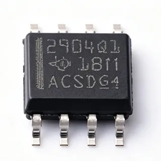
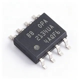
TLV2772CD - Dual 5.1MHz RRIO Amplifier | Texas Instruments
MPN: TLV2772CD ✓ Hoạt độngTLV2772CD Tóm tắt
An operational amplifier is a voltage-gain building block used to amplify small sensor and control signals, buffer imperfect sources, implement active filters, and drive analog-to-digital converter inputs. The TLV2772 belongs to the CMOS operational amplifier hierarchy, combining low power consumption with the bandwidth and slew rate needed for higher-speed signal chains. Its rail-to-rail output allows the output voltage to approach the supply rails more closely than a conventional fixed-output amplifier.
Key features include a 5.1 MHz unity-gain bandwidth, 10.5 V/µs slew rate, and 1 mA supply current per channel. The dual configuration provides two amplifiers in one package, reducing board area for paired signal paths. Shutdown support can reduce supply demand when the amplifiers are not needed, although operating behavior during shutdown requires verification against the manufacturer datasheet. The 8-pin SOIC package is also compatible with conventional surface-mount assembly methods.
The TLV2772 family combines high bandwidth, high output drive, rail-to-rail output swing, and good DC precision. Its 10.5 V/µs slew rate gives it substantially more dynamic range than slower general-purpose CMOS amplifiers, making it useful for pulse, waveform, and feedback-control applications. The 5.1 MHz bandwidth supports closed-loop operation at frequencies suitable for audio, communications, industrial measurement, and embedded analog interfaces.
Typical uses include portable sensor conditioning, low-voltage data-acquisition channels, active audio filters, motor and actuator feedback networks, and general-purpose buffering. The device is especially relevant where a designer needs faster edge rates than conventional low-power amplifiers while retaining roughly 1 mA of supply current per active channel. Rail-to-rail output operation also expands usable output range in systems operated close to the positive supply limit.
Designers should verify input common-mode limits, output-current capability, noise, offset voltage, and shutdown timing before finalizing a circuit. Keep feedback-loop compensation appropriate for the selected closed-loop gain, provide stable reference and feedback paths, and use short, low-impedance routing where high-frequency behavior matters. Decoupling capacitors should be placed close to the supply pins to minimize supply noise and local impedance.
This product page combines manufacturer specifications, practical application guidance, lifecycle information, and pin-level design references. It also identifies the technical distinctions that matter when evaluating this amplifier against same-package alternatives, including bandwidth, supply current, shutdown behavior, precision, and qualification requirements.
Bộ thay thế dễ dàng lắp đặt cho TLV2772CD — cùng gói, chân-to-chân tương thích. Các bộ phận yêu cầu hàn PCB bị loại trừ.
TLV2772AID
✅ Drop-In📋 Tham chiếu thay thế (không có trong danh mục)
TLV2772CD Tỷ lệ tối đa & tính chất điện
| Number of Amplifier Channels | 2 channels |
| Maximum Supply Voltage | 5.5 V |
| Minimum Operating Supply Voltage | 2.7 V |
| Unity-Gain Bandwidth | 5.1 MHz |
| Slew Rate | 10.5 V/µs |
| Supply Current per Channel | 1 mA |
| Output Topology | Rail-to-rail output |
| Process Technology | CMOS |
| Shutdown Function | Yes |
| Số lượng chân | 8 pins |
| Hộp | SOIC-8 (D) |
| Kiểu lắp đặt | Surface mount |
Cấu hình chân TLV2772CD
| Chân 1 | OUTA — Channel A output |
| Chân 2 | IN A- — Channel A inverting input |
| Chân 3 | IN A+ — Channel A non-inverting input |
| Chân 4 | SHUTDOWN — Device shutdown control |
| Chân 5 | IN B+ — Channel B non-inverting input |
| Chân 6 | IN B- — Channel B inverting input |
| Chân 7 | OUTB — Channel B output |
| Chân 8 | V+ — Positive supply connection |
Ứng dụng tiêu biểu
TLV2772CD phù hợp cho 6 Áp dụngs: Portable Sensor Signal Conditioning, Active Audio Filtering, Industrial Process Measurement, Data Acquisition Buffering, Motor Feedback Control, Communication Signal Conditioning.
Portable Sensor Signal Conditioning
The TLV2772CD suits portable sensor interfaces because each channel combines approximately 1 mA of supply current with 5.1 MHz bandwidth and 10.5 V/µs slew rate. It can amplify or buffer outputs from low-level sensors before conversion by an ADC, while its 2.7 V to 5.5 V operating range supports compact battery-powered electronics. Rail-to-rail output operation provides more usable signal range than a fixed-output amplifier when the supply rail is only slightly above the target level. The two channels can process complementary or differential signals, although input common-mode range, offset, and noise must be checked against the sensor output before final circuit closure.
Được đề xuất
Active Audio Filtering
The TLV2772CD can implement active audio filters because its 10.5 V/µs slew rate preserves large-signal response while its 5.1 MHz unity-gain bandwidth exceeds the bandwidth of many audio-band filter stages. The rail-to-rail output is useful in single-supply systems where conventional output limits would reduce signal symmetry. Both amplifier channels may form a second-order filter, a multiple-feedback stage, or a buffered tone-control network. Component selection must account for closed-loop stability, gain-bandwidth margin, distortion, noise, and the output load so that the selected filter topology does not approach the amplifier's stability or drive limits.
Được đề xuất
Industrial Process Measurement
The TLV2772CD is appropriate for industrial process-measurement front ends that need more bandwidth than a basic micropower amplifier while operating from a compact low-voltage supply. Its 5.1 MHz bandwidth handles faster sensor transients, and the 10.5 V/µs slew rate supports responsive feedback-control or waveform reconstruction stages. The dual package allows one channel to amplify the sensor signal and the other to provide an active filter or reference buffer. Field-isolated equipment should account for surge, ESD, noise, and common-mode transients through external protection, while the amplifier's input range and output drive are verified against the selected sensor and ADC interface.
Được đề xuất
Data Acquisition Buffering
The TLV2772CD can serve as a high-speed input buffer between a sensor or transducer and an ADC in a compact data-acquisition design. Its 5.1 MHz unity-gain bandwidth provides more closed-loop bandwidth than conventional low-power amplifiers, and its high slew rate drives the changing input levels more effectively into the ADC's sampling network. Rail-to-rail output operation helps maximize the available signal range in low-voltage systems. In practice, the source impedance, ADC acquisition time, capacitive loading, settling behavior, and output-current requirements must be checked together. Feedback and compensation components should be placed close to the amplifier to minimize parasitic effects during high-frequency operation.
Được đề xuất
Motor Feedback Control
The TLV2772CD can be used in current-feedback and voltage-feedback loops where fast amplifier dynamics improve responsiveness. Its 10.5 V/µs slew rate reduces the delay associated with large control-signal transitions, while 5.1 MHz unity-gain bandwidth supports higher loop bandwidth than a slow general-purpose amplifier. The dual package can place one channel in the control loop and the other in a supervisory or feed-forward path. Motor environments introduce wide-band switching noise and ground bounce, so filtering, grounding, output-current capability, and common-mode limits require careful review. Stable compensation is essential to prevent the high AC performance from producing ringing or instability in the completed loop.
Được đề xuất
Communication Signal Conditioning
The TLV2772CD is useful in low-voltage communication modules for amplifying, filtering, or reshaping burst signals before digitization. Its 5.1 MHz bandwidth and 10.5 V/µs slew rate provide adequate dynamic range for many baseband signal-conditioning tasks, while approximately 1 mA per channel helps constrain system power in portable equipment. The shutdown function can support power-saving strategies when a receiver or transmitter section is inactive. Designers should compare the amplifier's noise and distortion against the signal budget, place decoupling close to the power pins, and maintain a controlled return path because high-frequency switching edges can couple between the communication channel and adjacent circuitry.
Được đề xuất
Tóm tắt các sản phẩm được đề xuất
Dữ liệu tham khảo kỹ thuật cho TLV2772CD — so sánh, hướng dẫn thiết kế và thông tin tuân thủ.
Hướng dẫn chọn lựa
So sánh với các sản phẩm thay thế
| Tham số | Sản phẩm này | TLV2772AID |
|---|---|---|
| Package | SOIC-8 (D) | SOIC-8 (D) |
| Brand | Texas Instruments | Texas Instruments |
| Amplifier Channels | 2 channels | 2 channels |
| Maximum Supply Voltage | 5.5 V | 5.5 V |
| Minimum Operating Supply Voltage | 2.7 V | 2.7 V |
| Unity-Gain Bandwidth | 5.1 MHz | 5.1 MHz |
| Slew Rate | 10.5 V/µs | 10.5 V/µs |
| Supply Current per Channel | 1 mA | 1 mA |
| Output Topology | Rail-to-rail output | Rail-to-rail output |
| Shutdown Function | Yes | Yes |
Bảo phân biệt quan trọng
- Combines low channel current with high-speed dynamic performance (vsTLV2772AID)
- Dual-channel integration reduces board-space requirements (vsTLV2772AID)
- Rail-to-rail output supports low-voltage signal range (vsTLV2772AID)
Ghi chú thiết kế
Place the supply bypass capacitor as close as practical to the V+ connection and route it using a short, low-impedance path. Because the TLV2772 family combines 5.1 MHz bandwidth with 10.5 V/µs slew rate, long supply traces can introduce parasitic inductance and destabilize high-frequency operation. Keep the feedback components and non-inverting input connections compact, and maintain a continuous return path beneath the circuit to reduce susceptibility to switching and motor-drive noise.
Do not treat every member of the TLV277x family as an automatic replacement. The TLV2772 includes shutdown functionality, while related family members can differ in shutdown-pin behavior or omit shutdown entirely. A substitute must preserve the SOIC-8 footprint, pin functions, supply range, bandwidth, output drive, and stability behavior. Recheck the feedback network and shutdown logic after any device change instead of assuming that a matching package guarantees electrical compatibility.
Account for the full 5.1 MHz bandwidth when designing the signal chain rather than evaluating only midband gain. High-speed edges can excite capacitive inputs and long PCB traces, so keep sensitive nodes short and provide local return paths. For ADC interfaces, verify source impedance, ADC acquisition time, output settling, and capacitive load. For active filters, evaluate gain-bandwidth and phase-margin margins at the highest intended frequency and component tolerance.
Estimated: with a 5.5 V supply and 1 mA supply current per channel, the nominal device supply consumption is approximately 2 mA for both channels before output-current and shutdown-state effects. Use 5.5 V as the maximum supply value in worst-case rail analysis, and account separately for bias current and output load. Confirm shutdown-state current from the manufacturer datasheet before using the shutdown function for a strict power-saving budget.
Thông tin tuân thủ
The manufacturer product page confirms RoHS and REACH lead finish options, but no explicit compliance result was identified for the TLV2772CD orderable MPN. AEC-Q100 qualification is not indicated for this standard industrial device.