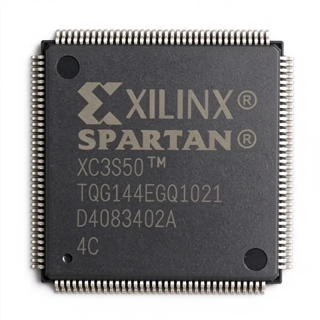
The XC3S50-4TQ144C is an AMD Spartan-3 field-programmable gate array with 50,000 system gates, 1,728 logic cells, 192 logic array blocks, 97 user I/Os and 73,728 RAM bits in a 144-LQFP square gull-wing package. It runs from a 1.2 V core supply, uses 90 nm process technology, carries the -4 speed designation and the commercial (C) temperature grade, and lists a 630 MHz maximum clock frequency. XAIPART stocks 12,000 units with MOQ 1, priced from $45.9375/unit at 1,000 pieces as of 2026-11-02. Buy the XC3S50-4TQ144C product page listing for live stock and quote options. This guide covers verified specifications, design-in practices, comparison against same-family candidates such as the XC3S50A-4TQ144C and XC3S50-5TQG144C, and sourcing risk notes engineers need before committing a layout.
What Is the XC3S50-4TQ144C and Which Specifications Are Verified?
The XC3S50-4TQ144C is the smallest density member of the Spartan-3 FPGA family from AMD, packaged in a 144-terminal LQFP with a square gull-wing form. An FPGA is a semiconductor whose logic, interconnects and dedicated resources are configured after manufacture, so one device can implement parallel control logic, state machines, protocol interfaces and data-processing pipelines without a fixed-function mask set. Unlike an ASIC, you can revise the logic by reprogramming the part.
The verified specification set is:
| Parameter | XC3S50-4TQ144C (verified) |
|---|---|
| Device Type | Field Programmable Gate Array (FPGA) |
| FPGA Family | Spartan-3 |
| System Gates | 50,000 gates |
| Logic Cells | 1,728 |
| Logic Array Blocks / CLBs | 192 |
| RAM Bits | 73,728 bits |
| User I/O | 97 |
| Core Supply Voltage | 1.2 V |
| Package | 144-LQFP, square gull-wing TQFP |
| Terminal Count | 144 terminals |
| Process Technology | 90 nm |
| Speed Grade | -4 |
| Temperature Grade | Commercial (C) |
| Maximum Clock Frequency | 630 MHz (listed; confirm against datasheet conditions before design use) |
| RoHS / REACH Status | unknown in verified database |
Two specification fields are not exposed in the verified data: the exact operating temperature range and the supported I/O standards. Confirm both against the manufacturer datasheet PDF before design release. Do not infer bank voltages, timing parameters or pin-level electrical ratings from the summary table above.
Takeaway: treat the table above as the contract. If a design decision needs a number that is not in it, pull it from the datasheet, never from memory or third-party summaries.
How Do You Design In the XC3S50-4TQ144C?
Design-in starts with three verified anchors: the 1.2 V core supply, the 97 available user I/Os and the 73,728-bit internal RAM budget. Everything else in your board and firmware plan must fit inside those limits.
Power architecture. The 1.2 V core rail is the primary supply requirement. The verified listing notes that pairing it with appropriate I/O voltage selection can simplify power architecture, but bank-specific voltage and decoupling guidance must follow the manufacturer datasheet. The verified data does not state the supported I/O standards or bank voltage options, so derive each I/O bank rail from the datasheet rather than assuming 3.3 V or 2.5 V operation. Design your regulator budget around worst-case core current at your actual clock activity, which requires datasheet power tables, not the headline clock figure.
Resource budgeting. With 1,728 logic cells across 192 logic array blocks, the device supports concurrent datapaths and moderate control complexity. Map your design early: state machines, bus interfaces and small fixed-point pipelines fit comfortably; anything requiring large FIFOs or wide multipliers will exhaust the 73,728 RAM bits quickly. At 73,728 bits total, a single 9K-bit dual-port block pattern means only a handful of independent buffers exist, so plan buffering hierarchies before writing HDL.
I/O planning. Ninety-seven user I/Os of the 144 terminals are available to logic. Reserve margin for configuration, clocking and dedicated functions, because the final pin count available to a design varies with configuration and dedicated-function requirements. The full numbered pin map is not exposed in the verified database, so the complete pin table on the product page and the datasheet pinout chapter are mandatory references before pin assignment.
Timing closure. The 630 MHz maximum clock frequency appears in a comparison listing, and the verified record itself flags that this value requires confirmation against the relevant datasheet condition before design use. The -4 speed grade constrains achievable fabric clocks well below that figure in practice; establish clock, setup, hold and I/O timing from the manufacturer family documentation and your routed design, not from the nominal listing.
Assembly. The 144-LQFP square gull-wing footprint suits conventional multilayer PCB assembly and rework. Its fine pitch requires controlled soldering and inspection per your assembly process qualification.
Configuration and unused pins. The verified data does not expose the configuration interface details or unused-pin requirements. Follow the datasheet's configuration and unused-pin chapters exactly; floating unused I/O on a legacy FPGA is a common field-failure cause.
Takeaway: lock three numbers first — 1.2 V core, 97 user I/Os, 73,728 RAM bits — then pull bank voltages, configuration and timing directly from the datasheet PDF before releasing layout.
What Are the Alternatives to the XC3S50-4TQ144C and How Do They Compare?
No verified drop-in replacement can be declared from the supplied cross-reference data. Two same-family candidates appear in the verified record, and both require firmware-, timing- and pin-level review before substitution. The verified comparison data shows:
| Parameter | XC3S50-4TQ144C | XC3S50A-4TQ144C (Spartan-3A) | XC3S50-5TQG144C |
|---|---|---|---|
| Family | Spartan-3 | Spartan-3A | Spartan-3 |
| Package | 144-LQFP | 144-LQFP | 144-TQFP |
| Logic Cells | 1,728 | 1,584 | [not stated in verified data] |
| RAM Bits | 73,728 | 55,296 | [not stated in verified data] |
| Speed Grade | -4 | -4 | -5 |
| Core Supply | 1.2 V | [not stated in verified data] | [not stated in verified data] |
XC3S50A-4TQ144C. It shares the 144-LQFP format but belongs to the Spartan-3A family with a different architecture: 1,584 logic cells and 55,296 RAM bits versus 1,728 logic cells and 73,728 RAM bits on the Spartan-3 part. Different family, different resource count — treat it as a redesign candidate, not a drop-in.
XC3S50-5TQG144C. Same package format and family, but the -5 speed grade changes timing. Additionally, the verified data does not define the C versus G order-code meanings, so temperature grade and supply specification must be confirmed against AMD ordering information before treating the suffix change as drop-in.
Cross-brand candidates. No cross-brand drop-in alternative is verified. Programming files, configuration startup, I/O behavior, voltage classes and timing margins are FPGA-specific; an equal package name alone establishes nothing. Any cross-brand candidate must be backed by explicit pin mapping, resource equivalence and timing verification.
Takeaway: if you must second-source, run the full pin map, timing report and bitstream regeneration against whichever candidate you pick — the verified data supports no plug-compatible swap.
What Is the Market Position, Lifecycle Status and Supply Situation?
The verified database contains two lifecycle statements that conflict, and both are stated here explicitly rather than averaged:
- The product record's lifecycle field lists the XC3S50-4TQ144C as active.
- The verified FAQ conclusion states it should be treated as obsolete for new production planning, based on the age of the Spartan-3 family and the absence of a current AMD lifecycle statement — not on a quoted manufacturer status.
Resolution for purchasing: the verified search set provides no current AMD lifecycle statement, so the active flag reflects database status rather than confirmed manufacturer endorsement. The prudent reading is that supply exists today but carries end-of-life risk for any new design.
Supply situation from verified XAIPART data as of 2026-11-02: 12,000 units in stock, MOQ 1. Pricing tiers: $78.75 at qty 1, $56.875 at qty 10, $50.3125 at qty 100, $48.125 at qty 500, and $45.9375 at qty 1,000. The verified FAQ also notes that a DigiKey search snippet said the product could ship the same day, but that snapshot carried no dated quantity, so third-party availability should be confirmed in writing before scheduling production. Because this is legacy programmable logic, the FAQ warns inventory may be limited or counterfeit-prone; request lead time with the exact MPN, quantity, date code and lot traceability.
RoHS and REACH status are unknown in the verified database — a compliance gap that matters for EU-bound builds and must be closed with the supplier or manufacturer before orders.
Takeaway: XAIPART's 12,000-unit stock makes immediate production viable, but the conflicting lifecycle evidence means any new design should carry a migration plan, and every order should demand date-code and lot traceability.
What Trends Should Buyers and Engineers Watch?
1. Legacy-toolchain dependency. The Spartan-3 family is a mature 90 nm generation. Verified applications guidance flags obsolete-family tooling and supply continuity as the main risks for long-lifecycle equipment such as test instrumentation. Verify that your current software toolchain still supports the device before committing multi-year programs, and archive tooling versions now.
2. Pricing spread signals allocation risk. The spread from $78.75 (qty 1) to $45.9375 (qty 1,000) as of 2026-11-02 is roughly 42% between single-unit and volume pricing — typical of constrained legacy stock where broker supply dominates the margin. Lock volume pricing early if you need more than a few hundred units per year, and expect price movement as the 12,000-unit pool depletes.
3. Design-fit discipline matters more than headline speed. The 630 MHz maximum clock listing requires confirmation against datasheet conditions, and verified applications guidance repeatedly directs engineers to derive throughput from actual routing and timing rather than the nominal figure. For new precision or data-acquisition designs, the verified guidance is to validate converter compatibility, grounding and analog isolation explicitly.
4. Compliance verification is outstanding. Unknown RoHS and REACH status plus an unconfirmed operating temperature range are open items. Close both before any order that touches regulated markets or wide-temperature environments.
5. New designs should default to supported silicon. The verified FAQ is direct: for new high-volume or long-lifecycle designs, a currently supported FPGA with more I/O, faster interfaces, larger memory and modern tooling is generally preferable. Reserve the XC3S50-4TQ144C for continuity of existing Spartan-3 designs where a verified 144-LQFP layout and qualified supply make continuity more valuable than modern-device benefits.
Takeaway: buy from the verified stock listing with traceability, archive your toolchain, and start any genuinely new design on current-generation silicon. For broader component research, browse the XAIPART component catalog or read the XAIPART blog; related deep dives include the ADC0804LCJ ADC guide and the 9FGL0851CKILF clock generator guide.
留言
成為第一個留言的人。
🔐 請 登入 即可送出留言。
還沒有帳戶嗎? 註冊