STM32G031C8T7
STM32G031C8T7 - 64MHz Cortex-M0+ MCU | STMicroelectronics
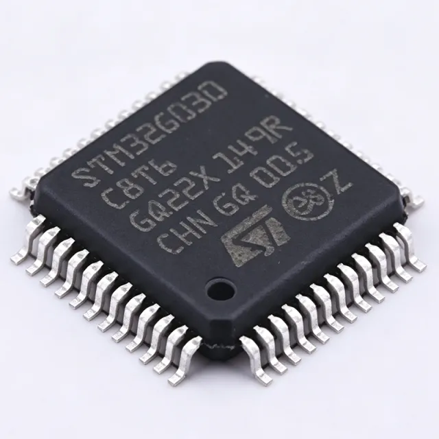
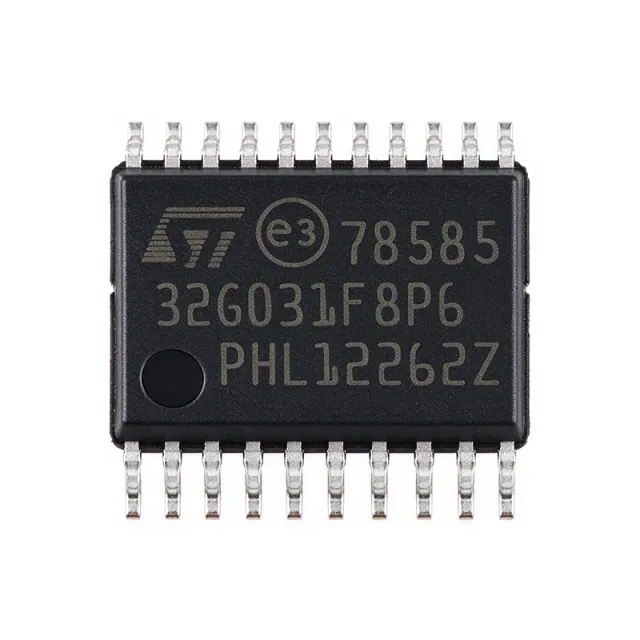
The STMicroelectronics STM32G031C8T7 is a 32-bit Arm Cortex-M0+ microcontroller operating at up to 64 MHz, with 64 KB of Flash memory and 8 KB of SRAM, housed in a 48-pin LQFP 7 x 7 mm package. The device is positioned for compact embedded-control systems that require efficient real-time processing, mixed-signal measurement, timer-driven control, and serial connectivity without the complexity of a higher-performance Cortex-M core.
A microcontroller is a programmable semiconductor that integrates a processor core, memory, analog and digital peripherals, and communication interfaces onto one device. The STM32G0 family belongs to the broader embedded-controller hierarchy: Arm Cortex-M0+ core, 32-bit microcontroller, embedded processor, and system-on-chip. Its compact architecture is intended for cost-sensitive products in which deterministic control, low component count, and flexible peripheral integration matter more than high-end graphics or large memory capacity.
The STM32G031C8T7 combines a 64 MHz Arm Cortex-M0+ processor with 64 KB of Flash and 8 KB of SRAM. The listed connectivity capabilities include I2C, SPI, UART, IrDA, LIN bus, and Smart Card interfaces. Forty-four I/O pins provide connections for sensors, actuators, displays, communications, and control signals. Operation from 2.5 V and 3.3 V supply rails also supports both conventional embedded-system voltages found in industrial, consumer, and instrumentation equipment.
The STM32G031x4, STM32G031x6, and STM32G031x8 devices share the Arm Cortex-M0+ platform, while their memory capacities and peripheral resources differ by density grade. The x8 designation in STM32G031C8 corresponds to the 64 KB Flash variant shown in the product listing. The C package code identifies the 48-pin configuration, while the T7 ordering code identifies the specified temperature and package arrangement associated with this ordering code.
Typical applications include low-cost sensor nodes, compact motor and timer-control boards, industrial monitoring instruments, communication modules, and mixed-signal control products. Designers can use the analog-to-digital conversion, timer, PWM, and serial interface resources to consolidate functions that otherwise require separate analog, timing, and communication components. The 48-pin LQFP also provides more I/O access than smaller packages while remaining inspectable and repairable by conventional leaded-assembly methods.
Layout planning should prioritize short, continuous supply and ground paths around the microcontroller, especially around analog inputs and external interfaces. Decoupling capacitors should be placed directly beside their associated power pins, while oscillator and high-speed signal routes should avoid crossing noisy switching paths. Firmware changes between MCU families should be reviewed against peripheral availability, interrupt behavior, memory layout, and pin multiplexing before production use.
This product record combines manufacturer device information, distributor specifications, package characteristics, replacement guidance, and practical design notes. It is intended to help engineers determine whether the STM32G031C8T7 matches the required core performance, memory capacity, I/O count, interface set, package, and operating environment before committing a design to production.
詢價
聯絡我們