產品(39,000+)

AM26LS31CN - Quad RS-422 Differential Driver | Texas Instruments
AM26LS31CN

AM26LS31CN - Quad RS-422 Differential Driver | Texas Instruments

The Texas Instruments AM26LS31CN is a quadruple complementary-output differential line driver with four independent driver channels, designed for ANSI TIA/EIA-422B and ITU V.11 balanced digital transmission. It is supplied in a 16-pin dual in-line package, and the verified distributor listing identifies it as an RS-422/RS-485 interface driver. Each channel provides differential outputs for driving balanced digital lines while helping reject common-mode noise present in industrial and telecommunications environments. A differential line driver is an interface IC that converts a single-ended logic signal into two complementary signals. The receiver at the far end interprets the voltage difference between those signals as the transmitted bit. This approach improves noise immunity compared with a single-ended link and allows reliable communication over longer cable runs when the driver, receiver, termination, and cable characteristics are correctly matched. The AM26LS31 belongs to the broader line-driver and digital-interface hierarchy. The AM26LS31CN family provides four channels in one package, reducing component count and simplifying point-to-point or multidrop RS-422 interface designs. Its complementary outputs are intended for balanced line operation, while the driver-side logic interface connects to a digital controller, transmitter, or test system. Because the verified results identify the device as a quadruple line driver but do not provide complete electrical tables, values such as output voltage, propagation delay, supply current, and temperature limits are retained as data-needed items rather than estimated. Typical uses include industrial control links, instrumentation, communications equipment, test systems, and embedded data transmission where balanced signaling is preferred. Four channels allow the same package to support multi-wire links or several independent point-to-point connections. In practice, the receiving device should provide the complementary differential inputs, and the physical layer should follow the applicable cable and termination requirements. A critical design consideration is confirming that the receiver, cable, and termination scheme are appropriate for the intended RS-422 application. Keep the line-driver outputs routed as a matched differential pair, minimize unnecessary stubs, and provide a suitable ground/reference strategy. The 16-pin through-hole package is also mechanically different from modern surface-mount options, so a replacement is only drop-in when both the footprint and pinout are identical. This page combines the verified manufacturer and distributor links, package and interface information, practical application guidance, and a strict comparison of only same-footprint drop-in candidates. It does not infer electrical specifications or lifecycle claims that were not present in the supplied data.

詢價 聯絡我們
AM26LV32IDR - 32MHz 3.3V Quad RS-422 Receiver | TI
AM26LV32IDR

AM26LV32IDR - 32MHz 3.3V Quad RS-422 Receiver | TI

The Texas Instruments AM26LV32IDR is a low-voltage, high-speed quadruple differential line receiver with four independent receivers, 3-state outputs, and a 16-pin SOIC package. It operates from a single 3.0 V to 3.6 V supply, supports switching rates up to 32 MHz, and is designed for balanced bus transmission similar to TIA/EIA-422-B and ITU Recommendation V.11 receivers. A differential line receiver is an interface circuit that converts a balanced differential signal into a single-ended logic signal while rejecting common-mode noise. In the interface hierarchy, it belongs to the receiver class of RS-422 interface ICs, which sit between a physical communication bus and digital logic. The AM26LV32IDR is optimized for low-voltage, high-speed point-to-point or multidrop communication where four channels must be received in one package. Key features include four differential receivers, a common enable control for all outputs, and 3-state output capability for bus isolation. The BiCMOS architecture combines low power dissipation with high switching performance. The device is specified for a 3.3 V supply, making it suitable for systems whose digital core operates from the same voltage rail. Its 32 MHz maximum switching rate supports substantially faster signaling than conventional low-speed RS-422 receivers. The AM26LV32 family is intended for balanced differential buses and point-to-point data links. Its reduced common-mode voltage range is a consequence of the low supply voltage, so the complete bus voltage and grounding plan must remain within the device's specified operating limits. The common enable function allows the receiver outputs to enter a high-impedance state when the host needs to isolate the interface. Typical uses include industrial automation equipment, test and measurement instruments, computer peripherals, data acquisition systems, and multi-channel communication links. Because each channel is independent, the IC can also serve monitoring, redundant sensing, or distributed input systems where four differential signals share a common supply. When laying out a board, keep the differential traces short, matched, and continuous over a common ground reference. Place receiver bypass capacitors close to the supply pins and follow the manufacturer's recommended termination and protection practices. Verify that the driver, cable, connector, and receiver common-mode limits remain compatible across temperature and supply tolerance. This page combines the verified manufacturer, distributor, and cross-reference data with practical interface selection guidance, package information, and design notes that are not presented as a simple replacement for the complete TI datasheet.

詢價 聯絡我們
AM3352BZCZ100 - ARM Cortex-A8 1GHz Sitara MPU | TI
AM3352BZCZ100

AM3352BZCZ100 - ARM Cortex-A8 1GHz Sitara MPU | TI

The Texas Instruments AM3352BZCZ100 is a Sitara ARM Cortex-A8 microprocessor (MPU) running at 1.0 GHz in a 324-ball NFBGA (ZCZ, 15x15 mm) package, rated for 0C to 90C operation, with integrated 1Gb Ethernet, display controller, and CAN peripherals for embedded industrial designs. A microprocessor (MPU) is a single-chip central processing unit that executes operating-system-level software from external memory. Within the semiconductor hierarchy, the AM3352 belongs to the Sitara MPU family, then ARM application processors, then embedded processors, then semiconductors. MPUs like the AM3352 bridge the gap between microcontrollers and high-end application processors by pairing an ARM Cortex-A8 core with microcontroller-class peripherals, enabling Linux-class software with industrial I/O on one chip. Key features include the 1.0 GHz 32-bit ARM Cortex-A8 RISC core with NEON SIMD coprocessing and 256 KB L2 cache, a 1Gb Ethernet MAC for high-speed networking, LCD display support for human-machine interfaces, and CAN for industrial fieldbus communication. The device supports high-level operating systems such as Linux and Android, with I/O operating at 1.8V/3.3V and an integrated MMU for virtual memory management. Technically, the AM335x platform integrates multiple UART, SPI, I2C, PWM, timer modules, and a 12-bit ADC around the core. The 324-ball NFBGA package provides strong thermal and electrical performance for 1 GHz-class operation, and TI supplies a complete Linux SDK with long-term support, reducing software development risk for industrial designs. Typical applications include factory automation controllers, HMI touchscreen panels, industrial networking gateways leveraging the 1Gb Ethernet and CAN interfaces, and portable test or medical equipment where low power meets embedded Linux requirements. When designing with the AM3352, follow TI power-sequencing and decoupling guidance in the AM335x datasheet; multi-rail power-up order and careful BGA fanout are essential for signal integrity at 1 GHz. This page synthesizes distributor pricing, drop-in alternative analysis, and practical design notes not found in the manufacturer datasheet.

詢價 聯絡我們
AM3354BZCZ80 - Sitara ARM Cortex-A8 MPU 800MHz | TI 324-NFBGA
AM3354BZCZ80

AM3354BZCZ80 - Sitara ARM Cortex-A8 MPU 800MHz | TI 324-NFBGA

The Texas Instruments AM3354BZCZ80 is a high-performance ARM Cortex-A8 32-bit microprocessor from the Sitara AM335x family, integrating 3D graphics acceleration, CAN, Ethernet, and dual PRU-ICSS industrial peripherals in a 324-pin NFBGA (ZCZ) 15x15 mm package. It operates at up to 800 MHz with NEON floating-point extension and a 32KB I-cache / 32KB D-cache plus 256KB L2 unified cache. What is a Sitara microprocessor? A Sitara microprocessor (MPU) is a high-integration 32-bit ARM Cortex-A system-on-chip designed by Texas Instruments for industrial, automotive infotainment, and human-machine interface (HMI) applications. Unlike microcontrollers (MCUs) that run firmware from internal flash, MPUs require external DDR memory and execute a rich operating system such as Linux. The Sitara family sits in the hierarchy MPU -> microprocessor -> processor -> integrated circuit, and bridges the gap between low-power MCUs and high-end application processors. Key features of the AM3354BZCZ80 include SGX530 3D graphics engine supporting OpenGL ES 2.0, two programmable real-time units (PRU-ICSS) for deterministic industrial protocols, dual 10/100/1000 Ethernet MACs, two USB 2.0 high-speed PHYs (host + device/host), six UARTs, two CAN controllers, three I2C ports, three SPI ports, and a 12-bit ADC. The integrated LCD controller supports up to 2048x2048 resolution, and the device is qualified for the 0 to 90 C commercial operating range as indicated by the absence of an industrial-grade temperature letter in the part number (the A100 variant covers -40 to 105 C industrial). The architecture combines a single Cortex-A8 core running Linux/WinCE/Android, the SGX530 GPU for graphics, and two 32-bit PRU cores that operate independently of the ARM core for real-time deterministic I/O - critical for industrial protocols such as EtherCAT, Profibus, and Sercos. External 16-bit DDR2/DDR3 memory interface supports up to 1 GB of RAM. Typical applications include industrial programmable logic controllers (PLC), human-machine interfaces (HMI), point-of-sale terminals, barcode scanners, smart grid concentrators, portable data terminals, and automotive infotainment head units. The integrated CAN and dual PRU make it especially attractive for industrial fieldbus gateways. When designing with this MPU, ensure the PCB uses a 4-layer stackup with a continuous ground plane beneath the NFBGA, a matched-length DDR2/DDR3 interface, and proper power-rail sequencing. The BGA requires X-ray inspection and reflow with peak temperature not exceeding 260 C per JEDEC J-STD-020. This page synthesizes distributor pricing, pin-compatible same-package alternatives, and practical design notes not found in the manufacturer datasheet alone.

詢價 聯絡我們
AM3357BZCZA80 - Sitara ARM Cortex-A8 800MHz MPU | TI
AM3357BZCZA80

AM3357BZCZA80 - Sitara ARM Cortex-A8 800MHz MPU | TI

The Texas Instruments AM3357BZCZA80 is a Sitara ARM Cortex-A8 microprocessor unit (MPU) operating at up to 800 MHz, integrating a single 32-bit core with NEON SIMD engine and a 324-pin NFBGA (15x15 mm) package. Per TI's AM335x datasheet, this silicon is part of the AM335x family that scales features across the Sitara line while retaining a pin-compatible BGA footprint on the 0.8 mm pitch 324-ball array, enabling PCB reuse across the family. The 'A80' speed grade and industrial temperature support make this specific part suited to harsh-environment industrial designs. An ARM Cortex-A8 MPU is a system-on-chip class microprocessor that integrates CPU core, memory controller, graphics, and a wide peripheral set into one BGA. In the taxonomy of computing devices it sits below an application processor SoC and above a microcontroller: an MPU lacks internal flash (relies on external DDR/NOR/NAND) but offers full MMU, OS support (Linux, Android, RTOS), and rich connectivity peripherals (Ethernet, USB, CAN, PRU-ICSS). The AM335x family is widely used as a Linux-capable industrial MPU for HMI, PLC, and gateway products. Key features of the AM3357 include a 32-bit ARM Cortex-A8 core with NEON, 200 MHz of MIPS-class performance headroom, two 32-bit DDR2/DDR3/DDR3L memory controllers with ECC, dual-port 1 Gbps Ethernet switch with IEEE 1588v2 support, two USB 2.0 high-speed ports (one OTG), and on-chip cryptography acceleration (AES, SHA, RNG). Graphics are handled by a programmable 24-bit LCD controller (up to 2048x2048) with touchscreen, and a separate 2D/3D graphics accelerator (SGX530) supports OpenGL ES 2.0. Technical depth: the AM3357 implements the Programmable Real-time Unit Subsystem (PRU-ICSS) with dual 32-bit RISC cores operating at 200 MHz, deterministic I/O latency, and direct access to peripheral pins - enabling industrial protocols such as EtherCAT, Profibus, and PROFINET entirely in firmware. The device is manufactured in a 65 nm process and supports separate 1.8 V / 3.3 V supply rails with on-die LDO/power-management ICs. Typical applications include industrial HMI panels, PLCs, motor drives, barcode scanners, portable data terminals, building automation gateways, and Linux-based IoT edge devices. The wide peripheral mix eliminates external companion chips for most designs. When designing with the AM3357, ensure the PCB stack-up supports 0.8 mm BGA escape routing, provision an external DDR2/DDR3 memory with matched-length traces, and follow TI's Power-Sequencing recommendations for the dual-voltage supply. This page synthesizes distributor pricing, drop-in cross-family alternatives, and PRU-ICSS design notes not found in the manufacturer datasheet.

詢價 聯絡我們
AM3357BZCZD60 - Sitara ARM Cortex-A8 MPU 600MHz | Texas Instruments
AM3357BZCZD60

AM3357BZCZD60 - Sitara ARM Cortex-A8 MPU 600MHz | Texas Instruments

The Texas Instruments AM3357BZCZD60 is a Sitara ARM Cortex-A8 32-bit microprocessor with integrated EtherCAT, PROFIBUS, PRU-ICSS and CAN support, operating at up to 600MHz and housed in a 324-ball NFBGA (15x15 mm) ZCZ package. As a member of TI's AM335x family, the AM3357BZCZD60 combines a single Cortex-A8 core running at 600MHz with two Programmable Real-time Units (PRU-ICSS), industrial protocol acceleration, and a rich peripheral set including two USB 2.0 ports, two Gigabit Ethernet MACs (one industrial-grade with two-port switch), and a 3D graphics engine. The device is qualified for an industrial -40C to +90C operating range and is targeted at deterministic real-time industrial communication. A microprocessor (MPU) is an integrated processing device that integrates a CPU core, memory controller, peripheral controllers and I/O into a single chip, distinguishing it from a microcontroller (MCU) which typically emphasizes on-chip Flash and simpler peripherals. Within the system hierarchy, an MPU sits above basic MCUs and below application processors in computational capability, providing the horsepower to run high-level operating systems such as Linux while maintaining the deterministic I/O needed for industrial control. The Sitara family specifically targets applications requiring a balance of high-level OS support and real-time industrial protocols on a single die. Key features include the Cortex-A8 core with NEON SIMD and VFPv3 floating-point hardware, 32KB L1 instruction and data caches, a 256KB L2 cache, a 32-bit LPDDR1/DDR2/DDR3/mDDR memory controller, two 12-bit ADCs, two USB 2.0 high-speed ports (with one capable of PHY interface), two industrial-grade CAN controllers, two PRU subsystems for deterministic I/O, a real-time clock, an SGX530 3D graphics accelerator, and a LCD controller with WXGA resolution support. The integrated EtherCAT slave controller and PROFIBUS support eliminate the need for an external ASIC, reducing BOM cost for industrial automation designs. The architecture is built on TI's 65nm CMOS process, supports ARMv7-A instruction set, and provides boot sources including SPI, MMC/SD, UART and NAND/NOR Flash. Power management is handled through multiple core voltage domains enabling dynamic frequency scaling and deep sleep modes with RTC retention. A typical 1.1V core supply and 3.3V I/O supply are required, with the integrated LDOs and PMIC companion devices managing the sequencing. Security features include a hardware crypto accelerator (AES, SHA, RNG) and secure boot support through the AM335x ROM bootloader. Typical applications include industrial programmable logic controllers (PLC), human-machine interfaces (HMI), point-of-sale (POS) terminals, industrial gateways, motor control drives with EtherCAT, machine vision systems, portable medical devices, and networked sensors with fieldbus connectivity. The dual-PRU subsystem is especially useful for custom industrial I/O protocols requiring sub-microsecond deterministic response without burdening the Cortex-A8 core. When designing with this device, pay close attention to the DDR3 memory trace impedance and length matching - the DDR3 interface requires careful signal integrity work. The PRU firmware should be developed using TI's PRU-RemoteProc and CCS toolchain. For EtherCAT or PROFIBUS applications, use TI's certified protocol stacks rather than reimplementing from scratch. Refer to TI's AM335x Hardware User Guide and the PRU-ICSS Reference Guide for detailed peripheral programming examples and reference schematics. This page synthesizes distributor pricing, drop-in alternatives, and practical design notes not found in the manufacturer datasheet alone.

詢價 聯絡我們
AM3358BZCE60 - Sitara ARM Cortex-A8 MPU 600MHz | TI
AM3358BZCE60

AM3358BZCE60 - Sitara ARM Cortex-A8 MPU 600MHz | TI

The Texas Instruments AM3358BZCE60 is a Sitara ARM Cortex-A8 microprocessor IC integrating a single 32-bit core running at 600 MHz, a POWERVR SGX530 graphics accelerator, dual PRU-ICSS (Programmable Real-Time Unit and Industrial Communication Sub-System) cores, and a rich industrial peripheral set, packaged in a 298-ball NFBGA (ZCE) measuring 13x13 mm. A microprocessor is an integrated circuit that contains one or more CPU cores along with caches, memory controllers, and on-chip peripherals, forming a complete system-on-chip (SoC) for embedded computing. The Sitara family occupies the mid-tier of TI's industrial-grade ARM processors, sitting above the Cortex-M based TM4C and below the Cortex-A9/A15 based OMAP and Jacinto families in terms of performance and integration. AM335x devices are differentiated from Cortex-M microcontrollers by their ability to run high-level operating systems such as Linux and Android. Key features of the AM3358BZCE60 include the ARM Cortex-A8 core with NEON SIMD engine, 32KB L1 instruction cache, 32KB L1 data cache, and 256KB L2 cache; an integrated 3D graphics accelerator supporting OpenGL ES 1.1/2.0; dual 32-bit PRU cores delivering deterministic real-time I/O; on-chip DDR3/LPDDR/LPDDR2/DDR2 memory controller; two industrial Gigabit Ethernet MACs (one with 2-port switch); USB 2.0 with PHY; CAN, SPI, I2C, UART, McASP, and eCAP peripherals. The device targets industrial communication protocols including EtherCAT, PROFIBUS, and PROFINET. Architecturally, the AM3358 pairs a single-issue, in-order Cortex-A8 with hardware graphics and a programmable real-time subsystem. The PRU-ICSS provides cycle-accurate I/O handling independent of the ARM core, enabling industrial protocol stack offload and low-latency fieldbus operation without burdening the HLOS. The ZCE NFBGA package is the lowest-cost AM3358 variant. Typical applications include industrial programmable logic controllers (PLL/PLC), human-machine interfaces (HMI), industrial gateways, barcode scanners, portable data terminals, automated test equipment, and consumer/educational embedded platforms such as the BeagleBone Black. The wide peripheral set also supports point-of-sale terminals and medical patient-monitoring equipment. When designing with this device, follow TI's PowerVR SGX530 driver support, ensure proper DDR3 PCB layout with controlled-impedance routing, and verify industrial protocol firmware availability for the target protocol. The ZCE package has a thermal pad that requires adequate PCB copper for heat dissipation.

詢價 聯絡我們
AM3874CCYE80 - Sitara ARM Cortex-A8 800MHz MPU | Texas Instruments
AM3874CCYE80

AM3874CCYE80 - Sitara ARM Cortex-A8 800MHz MPU | Texas Instruments

The Texas Instruments AM3874CCYE80 is a high-performance Sitara ARM Cortex-A8 microprocessor built on a 45 nm process, integrating one 32-bit core running up to 800 MHz along with NEON SIMD multimedia extensions and a SGX530 graphics accelerator. Housed in a 684-ball FCBGA (CYE) at 23x23 mm, this processor combines CPU, 3D graphics, an HDVPSS video subsystem, and HDMI output on a single die, replacing what traditionally took a CPU plus a discrete video processor. Industrial-grade temperature range is 0C to 90C. A microprocessor (MPU) is an integrated circuit that contains the arithmetic logic unit, control unit, and registers needed to execute software, typically paired with external DRAM, non-volatile storage, and peripherals. The AM3874 sits in the Sitara family of application processors — application processors are MPU subcategory with multimedia, graphics, and high-speed peripherals targeting HMI, industrial vision, and single-board computing workloads. Within TI's processor portfolio, AM3874 belongs to the Cortex-A8 generation that bridges ARM9 and Cortex-A9 performance classes. Key features include one ARM Cortex-A8 core at 800 MHz, ARMv7-A architecture with NEON SIMD coprocessor, a programmable SGX530 graphics core supporting OpenGL ES 1.1/2.0, integrated HDMI transmitter, dual DDR2/DDR3 memory controller up to DDR2-1066, a 10/100/1000 Mbps Gigabit Ethernet MAC, SATA 3 Gbps interface, two USB 2.0 ports (host + on-the-go), and HDVPSS for video encode/decode. Hardware-accelerated cryptography and a dual-core PRU-ICSS programmable real-time unit subsystem are integrated on-die. The AM3874's heterogeneous compute architecture lets the ARM Cortex-A8 host high-level operating systems like Linux while the PRU-ICSS offloads deterministic real-time I/O at sub-microsecond latency. The HDVPSS paired with HDMI 1.3a transmitter delivers 1080p60 display output without an external video encoder, and the SATA interface enables direct attachment of hard-disk or optical-storage subsystems in embedded computing platforms. Typical applications include industrial human-machine interface (HMI) panels, single-board computers, point-of-sale terminals, digital signage media players, medical imaging displays, and machine-vision controllers. The integrated HDMI and graphics pipeline makes it especially well suited for products that previously required a separate system-on-module plus a dedicated video co-processor. When designing with this part, allocate board area for the 684-ball FCBGA and follow TI's escape-routing guidelines for the BGA; the part demands a multi-layer PCB with continuous reference planes for the DDR2/DDR3 interface. Ensure proper thermal management — although the industrial temperature rating goes up to 90C ambient, sustained video workloads benefit from a heatsink or thermal interface material. This page synthesizes distributor pricing, drop-in alternatives, and practical design notes not found in the manufacturer datasheet, giving engineers a single, citable reference for selection.

詢價 聯絡我們
AM5728BABCXA - Dual Cortex-A15 1.5GHz Sitara MPU | Texas Instruments
AM5728BABCXA

AM5728BABCXA - Dual Cortex-A15 1.5GHz Sitara MPU | Texas Instruments

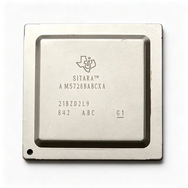
The Texas Instruments AM5728BABCXA is a Sitara microprocessor (MPU/SoC) integrating dual ARM Cortex-A15 cores at up to 1.5 GHz, dual C66x floating-point DSP cores, and a PowerVR SGX544 3D graphics accelerator, housed in a 760-ball FCBGA (ABC) package measuring 23x23 mm and rated from -40C to +105C for industrial environments. A microprocessor is a CPU integrated on a single chip that executes instructions and manages data flow in embedded computing systems. The AM5728 is a system-on-chip (SoC) that combines multiple heterogeneous processing cores (ARM and DSP) with memory controllers, peripheral interfaces, and graphics acceleration, forming the computational heart of an embedded system. It sits within the hierarchy: SoC -> microprocessor -> embedded processor -> integrated circuit. Key features include dual 1.5 GHz ARM Cortex-A15 cores for general-purpose OS workloads, dual C66x DSP cores for math-intensive signal processing, a dual-core PRU-ICSS for deterministic real-time industrial Ethernet protocols, DDR3/DDR3L memory support, HDMI and LCD display interfaces, and Gigabit Ethernet, USB 3.0, PCIe, and SATA connectivity. An integrated video acceleration engine handles H.264 encode/decode for multimedia pipelines. Architecturally, the AM5728 uses a heterogeneous multicore design supporting asymmetric (AMP) or symmetric (SMP) multiprocessing. ARM cores run Linux or RTOS workloads while DSP cores offload computationally heavy tasks; the PRU-ICSS provides deterministic low-latency I/O, optimizing performance per watt across diverse workloads. The 760-FCBGA (23x23) 0.8 mm-pitch ball grid array supports high gate density with strong signal integrity for high-speed DDR and SerDes interfaces. Typical applications include industrial PLCs, medical ultrasound systems, human-machine interfaces (HMI), smart grid gateways, and non-safety automotive infotainment - anywhere edge computing requires local processing plus rich connectivity. When designing with this device, ensure adequate multi-rail power delivery and thermal management, following the TI datasheet power-sequencing and decoupling recommendations for reliable operation across the full -40C to +105C industrial range. This page synthesizes distributor availability, drop-in alternatives from the AM57x family, and practical design notes not found in the manufacturer datasheet.

USD $42.50 聯絡我們
AM6528 Sitara MPU Dual Cortex-A53 + R5F 1.1GHz | TI
AM6528

AM6528 Sitara MPU Dual Cortex-A53 + R5F 1.1GHz | TI

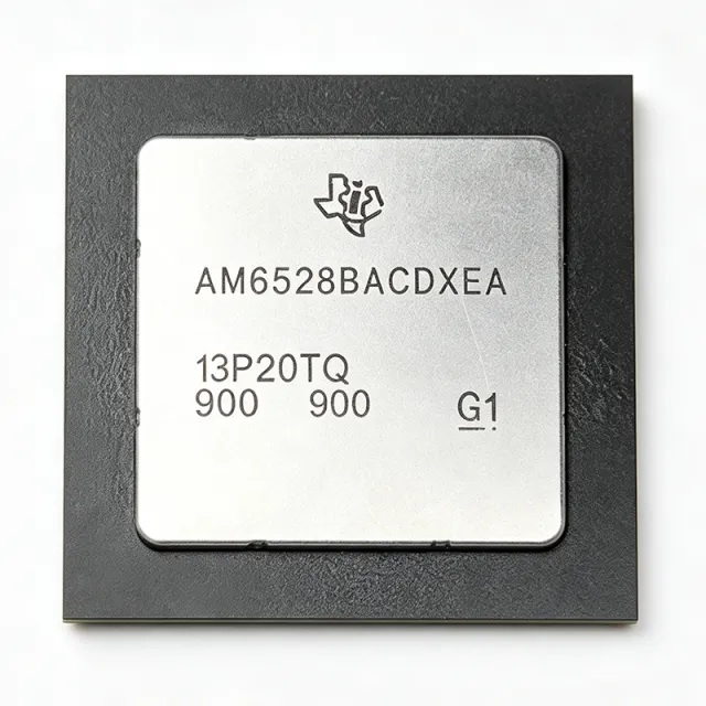
The Texas Instruments AM6528 is a Sitara applications processor featuring dual Arm Cortex-A53 cores running up to 1.1 GHz, dual lockstep-capable Arm Cortex-R5F cores at 400 MHz, a Gigabit PRU-ICSS for industrial Ethernet protocols, and integrated 3D graphics acceleration (SGX544). The AM6528BACDXEA variant ships in a 784-ball FCBGA package measuring 23x23 mm. An applications processor (MPU) is a high-performance system-on-chip designed to run a full operating system such as Linux, in contrast to microcontrollers (MCUs) that execute bare-metal or RTOS code. Within the embedded hierarchy, the AM6528 sits at: MPU -> applications processor -> embedded processor -> semiconductor, and occupies the mid-tier of TI's Sitara AM65x family between single-A53 parts and the quad-core AM6548. Key differentiating features include the heterogeneous dual Cortex-A53 + dual Cortex-R5F architecture, which lets Linux handle HMI, networking and connectivity while the R5F cores manage deterministic real-time control. The Gigabit PRU-ICSS offloads industrial protocols such as EtherCAT, PROFINET and EtherNet/IP from the main Arm cores, and the integrated 3D GPU enables graphics-rich HMI panels without an external display processor. The AM65x platform is built to meet the complex processing needs of Industry 4.0 embedded products, per TI's AM654x/AM652x datasheet (SPRSP52C, revised September 2023). Silicon revision 2.1 devices are currently shipping. TI's compare tool positions the AM6528 against the AM6548 and AM6442, with industrial communication software stacks and up to 5 Gigabit Ethernet ports available across the family. Typical applications include industrial HMI panels, PLCs, edge gateways, and motor-drive control systems where real-time determinism and Linux-level connectivity must coexist on a single silicon platform. Design consideration: the 784-FCBGA package demands careful PCB stackup planning; use TI reference designs such as the AM65x GP EVM for power sequencing, DDR4 routing and BGA escape routing guidance. This page synthesizes verified distributor pricing, drop-in family alternatives, and practical design notes not found in the manufacturer datasheet.

詢價 聯絡我們
AM6528BACDXEA - Dual Cortex-A53 1.1GHz Sitara MPU | TI
AM6528BACDXEA

AM6528BACDXEA - Dual Cortex-A53 1.1GHz Sitara MPU | TI

The Texas Instruments AM6528BACDXEA is a Sitara microprocessor (MPU) integrating dual Arm Cortex-A53 cores running at 1.1 GHz, a dual Arm Cortex-R5F MCU subsystem at 400 MHz, and Gigabit-class PRU-ICSS industrial communication subsystems, housed in a 784-pin FCCSP (ACD) package measuring 23x23 mm and rated for -40C to +105C operation. A microprocessor unit (MPU) is the central computation engine of an embedded system, sitting above microcontrollers (MCU) in the processing hierarchy but below application processors in complexity. Modern industrial MPUs like the AM6528 combine an applications-class Arm Cortex-A53 cluster for Linux-based software with a real-time Cortex-R5F lockstep-capable MCU subsystem, enabling a single chip to run both a high-level OS and deterministic real-time control tasks - a partitioning that previously required two separate devices. Key differentiating features include the PRU-ICSSG (Programmable Real-time Unit Industrial Communication Subsystem) with three Gigabit instances, supporting industrial Ethernet protocols such as EtherCAT, PROFINET, and EtherNet/IP in hardware with deterministic latency. A 3D graphics acceleration engine (SGX544 class) enables HMI and visualization workloads. The Cortex-R5F subsystem includes features intended to support functional-safety goals per the TI datasheet for the AM654x/AM652x family (Silicon Revision 2.1 documentation). Architecturally, the AM6528 belongs to the Sitara AM65x generation, built on TI's proven Cortex-A53/R5F heterogeneous multicore approach. The A53 cluster executes Linux or RTOS software, while the R5F cores handle time-critical control loops and safety monitoring, communicating through shared on-chip interconnect and memory subsystems. Typical applications include industrial PLCs and motor drive control heads, factory automation gateways with multi-protocol industrial Ethernet, HMI panels with 3D graphics, and building/energy automation controllers where -40C to +105C operation is required. When designing with this part, plan power sequencing for the multiple core rails and allocate DDR memory bandwidth carefully between the A53 and R5F subsystems; TI provides reference designs and power estimation tools in the AM65x documentation set. This page synthesizes distributor pricing, same-family drop-in alternatives, and practical design notes not found in the manufacturer datasheet.

USD $13.60 聯絡我們
AMC1300DWVR - ±250mV Reinforced Isolated Amplifier | Texas Instruments
AMC1300DWVR

AMC1300DWVR - ±250mV Reinforced Isolated Amplifier | Texas Instruments

The Texas Instruments AMC1300DWVR is a precision isolated amplifier that outputs a differential signal separated from its input side by a reinforced galvanic isolation barrier, offered in an 8-pin SOIC (DWV) wide-body package. The device accepts a differential input of ±250 mV and delivers a differential analog output with a fixed gain of 8.2, achieving ±0.3% (max) gain error and 1 mV input offset over its full operating range. Its isolation barrier is certified to VDE V 0884-11 and UL1577, providing reinforced isolation up to 5 kV RMS and a working voltage that suits motor drive, solar inverter, and grid-tie current-sensing stages. An isolation amplifier (also called an isolated current-sense amplifier) is a specialized analog component that combines a precision front-end amplifier with an integrated galvanic isolation barrier, allowing high-side shunt-resistor voltages to be measured safely from a low-voltage MCU or ADC domain. The category signal used for these parts sits inside the broader isolation IC family, which also includes digital isolators and isolated gate drivers, and the broader signal-chain hierarchy: isolation amplifier → instrumentation amplifier → op amp → analog IC. This positions the AMC1300 as a bridge between power-side analog signals and safety-isolated low-voltage digital control. Key features of the AMC1300DWVR include a 200 kHz small-signal bandwidth, 80 dB common-mode transient immunity (CMTI), ±1 µV/°C typical offset drift, and a low-side 3.3 V or 5 V single-supply operation. The fixed-gain architecture eliminates external resistor matching, while the integrated DC/DC-converter-friendly low-side supply simplifies BOM. The reinforced isolation barrier is implemented using TI's silicon-oxide (SiO2) capacitive isolation technology, providing long-term reliability and immunity to magnetic interference that would couple into opto-isolator or transformer alternatives. Typical applications include phase-current feedback for motor drives, DC-bus current sensing in solar inverters and string inverters, isolated voltage and current monitoring in grid-tie energy storage, EV traction inverter phase monitoring, and isolated analog front-ends for PLCs and industrial servo amplifiers. The ±250 mV linear input range is sized for standard 1 mΩ to 10 mΩ shunts, while the differential output drives a delta-sigma ADC such as the ADS131A04 or a SAR ADC with input common-mode flexibility. When designing with this device, ensure an isolated DC/DC converter powers the high-side input stage; the AMC1300 cannot generate its own high-side supply. Also confirm the local creepage/clearance on the PCB satisfies end-equipment IEC 61800-5-1 or IEC 60950 reinforced isolation rules. (page: 2026-10-06) This page synthesizes distributor inventory, fixed-gain alternatives, and isolation-barrier design notes that go beyond the bare datasheet.

詢價 聯絡我們
AMC1306M25 - ±250mV Reinforced Isolated Modulator | Texas Instruments
AMC1306M25DWVR

AMC1306M25 - ±250mV Reinforced Isolated Modulator | Texas Instruments

The Texas Instruments AMC1306M25 is a precision delta-sigma (ΔΣ) modulator optimized for shunt-resistor-based current sensing in high-voltage applications. It features a ±250-mV differential input range and a CMOS bitstream interface, with output separated from input circuitry by a capacitive double isolation barrier certified for reinforced isolation up to 7000 VPEAK per DIN EN IEC 60747-17 (VDE 0884-17) and UL1577. The device is packaged in an 8-pin wide-body SOIC (DWV) and operates from -40C to +125C. An isolated delta-sigma modulator is a type of analog-to-digital converter that oversamples the input signal and transmits a digital bitstream across an isolation barrier, where a digital sinc filter (typically in an MCU, DSP, or FPGA such as the TMS320F2800x C2000 family) reconstructs the measured current. In the power-management hierarchy it forms the front end of an isolated current-measurement chain: shunt resistor, isolated modulator, digital filter, current feedback for control loops. Key features include excellent DC accuracy: offset error of ±50 uV (max), offset drift of 1 uV/C (max), gain error of ±0.2% (max), and gain drift of ±40 ppm/C (max). The device delivers a 16-bit data stream at 78 kSPS (with a 10 MHz input clock) and provides 100 kV/us typical common-mode transient immunity (CMTI), making it robust in electrically noisy inverter environments. The AMC1306 family is pin-compatible across ±50-mV and ±250-mV input ranges and Manchester-coded or uncoded output options. The AMC1306M25 is ideal for motor control phase-current sensing, solar inverters, traction inverters, and industrial automation where accurate, galvanically isolated current measurement drives safety and efficiency. The capacitive isolation barrier resists magnetic interference, unlike transformer-based isolation. Design tip: place the shunt resistor close to the input pins with Kelvin connections to minimize parasitic inductance, and power the high-voltage side from a clean isolated 5V supply such as the UCC14240 iso-bias converter.

詢價 聯絡我們
AMC1336DWVR - ±1V Reinforced Isolated Delta-Sigma Modulator | TI
AMC1336DWVR

AMC1336DWVR - ±1V Reinforced Isolated Delta-Sigma Modulator | TI

The Texas Instruments AMC1336DWVR is a precision, reinforced-isolated delta-sigma (ΔΣ) modulator with a ±1-V differential input range and a capacitive double isolation barrier rated up to 8000 VPEAK, housed in an 8-pin wide-body SOIC (DWV) package. An isolated delta-sigma modulator is a type of analog-to-digital converter front end that oversamples an input signal and transmits a high-rate bitstream across a galvanic isolation barrier. Within the data-conversion hierarchy (isolated modulator -> ADC front end -> data acquisition IC -> signal chain), these devices allow voltage or shunt measurements to be made at high common-mode potentials while the digital controller remains on the safe side of the barrier. The AMC1336 belongs to TI's family of reinforced isolated amplifiers and modulators used across industrial, motor-drive, and energy infrastructure. Key features include the ±1-V input range optimized for direct resistor-divider voltage sensing, a capacitive isolation barrier highly resistant to magnetic interference, and certification for reinforced isolation up to 8000 VPEAK per DIN VDE V 0884-11 and UL1577. The 16-bit resolution at 82 kSPS output data rate suits feedback loops in power conversion. Technically, the device uses a second-order ΔΣ modulator on the high-voltage side and transmits the bitstream across the capacitive barrier, which rejects magnetic fields better than transformer-based isolation - important in inverter and motor-drive environments with high dV/dt and dI/dt. Typical applications include DC bus voltage sensing in solar inverters and motor drives, grid-tied energy-storage monitoring, and isolated voltage feedback in AC/DC power supplies. A key design consideration: the modulator bitstream must be decimated by an external digital sinc filter or on-chip filter of an MCU such as the SDFM peripheral - budget processing or peripheral resources accordingly. This page synthesizes distributor pricing context, drop-in alternatives, and practical design notes not found in the manufacturer datasheet.

詢價 聯絡我們
AMC3330DWER - ±1V Reinforced Isolated Amplifier | Texas Instruments
AMC3330DWER

AMC3330DWER - ±1V Reinforced Isolated Amplifier | Texas Instruments

The Texas Instruments AMC3330DWER is a precision, ±1-V input, reinforced isolated amplifier with an integrated isolated DC/DC converter, packaged in a 16-pin SOIC (DWE) wide-body package with 5 kV RMS reinforced isolation per IEC 60747-17. The device combines a differential input front-end optimized for high-impedance voltage sensing with a 2nd-order sigma-delta modulator followed by a digital isolation barrier and a single-ended analog output, providing a fixed differential gain of 2.0. An isolated amplifier (also called an isolation amp or iso-amp) is a specialized analog IC that uses an internal galvanic isolation barrier - typically based on capacitive or transformer coupling - to transmit an analog signal across a high-voltage domain while rejecting common-mode transients. Within the broader power-management signal-chain hierarchy, isolated amplifiers sit between the high-voltage sensing node (shunt resistor, resistor divider, or transducer) and the low-voltage controller (MCU, ADC, DSP), making them a subcategory of special-purpose amplifiers that bridges signal conditioning and functional safety. The AMC3330 belongs to TI's AMC33xx family of reinforced isolated amplifiers and is targeted at high-voltage system monitoring. Key features include ±1 V differential input range with 1.2 MΩ input impedance optimized for direct connection to high-impedance resistor dividers, ±0.2% maximum gain error, ±45 ppm/°C maximum gain drift, 86 dB minimum DC common-mode rejection ratio (CMRR), and a low-side single 3.3 V or 5 V supply thanks to the on-chip isolated DC/DC converter. A diagnostic output and fault-detection pin simplify system-level design, while the wide-body SOIC-16 (DWE) package provides >8 mm creepage/clearance for reinforced insulation. Architecturally, the AMC3330 integrates a 2nd-order sigma-delta modulator clocked internally, a digital isolation channel based on TI's capacitive SiO2 barrier technology, and an integrated flyback-style DC/DC converter that powers the high-side input circuitry from the low-side 3.3 V/5 V supply. The output is a differential analog voltage proportional to the differential input times the fixed gain of 2.0, with bandwidth and noise performance optimized for voltage (rather than current) sensing. Typical applications include high-voltage bus voltage monitoring in solar inverters, EV traction-inverter DC-link sensing, industrial motor-drive DC-bus measurement, UPS and battery-management system (BMS) voltage monitoring, and any precision non-ground-referenced voltage measurement where reinforced isolation is mandated by safety standards. The high input impedance eliminates the need for a high-side buffer op-amp, simplifying BOM. When designing with this device, place the sense resistor divider close to the INP/INN pins and keep the layout of both connections symmetrical to preserve CMRR. Decoupling capacitors must be placed as close as possible to the supply pins, and the low-side ground reference must be solid to avoid ground-loop noise coupling into the analog output. Because the device operates from a single low-side supply, no isolated bias supply is needed - this is a major BOM-saving advantage over discrete isolated-amplifier designs. This page synthesizes distributor pricing, drop-in same-brand and cross-brand pin-compatible alternatives, application guidance, and practical design notes not found in the manufacturer datasheet alone.

詢價 聯絡我們
APA075-FG144 - 75K Gate Flash FPGA, 180 MHz | Microchip Technology
APA075-FG144

APA075-FG144 - 75K Gate Flash FPGA, 180 MHz | Microchip Technology

The Microchip Technology APA075-FG144 is a ProASICPLUS flash-based field-programmable gate array with 75,000 system gates, a 180 MHz internal frequency, and 100 user I/Os in a 144-LBGA package. It combines CMOS programmable logic with on-chip flash configuration memory, allowing the device to retain its logic configuration without a separate configuration PROM. A field-programmable gate array, or FPGA, is a programmable-logic semiconductor whose interconnects and processing blocks can be configured after manufacture. Within the product hierarchy, an FPGA belongs to programmable logic, alongside CPLDs, while its physical construction uses CMOS logic fabric, flash memory, user I/O, and clocking resources. ProASICPLUS devices occupy the low-density programmable-logic segment and support reprogrammability combined with nonvolatile configuration retention. The APA075 part family provides 75,000 system gates, 180 MHz internal operation, and 3,072 cells according to the device comparison data. Its flash-based configuration architecture removes the need for external configuration memory and permits the design to be reprogrammed in the field. The APA075-FG144 exposes 100 user I/Os and uses a 1 mm pitch FBGA-144 package intended for compact surface-mount designs. The device is identified as a 144-pin CMOS FPGA in a 144-LBGA package. A second listing describes the same device as a 144-LBGA package with 100 I/Os, while the family documentation identifies the APA075 series as a ProASICPLUS Flash FPGA using a 0.22 µm CMOS process. These figures place the part in the low-density programmable-logic category rather than the high-performance FPGA class. Typical uses include protocol bridging, glue-logic consolidation, embedded control logic, legacy system upgrades, and industrial or communications equipment where a compact nonvolatile FPGA is preferable to a mask-programmed ASIC. Because the configuration is stored in flash, the design also remains functional after power cycling without an external loader sequence. The principal design consideration is that the FBGA-144 footprint requires a multilayer PCB, careful escape-routing, and thermal planning for the 0 to 70 C rated variant. Signal-integrity work should account for the 1 mm package pitch and clock distribution, while unused I/Os should be terminated according to the family guidance. Pin assignments and differential or clock-specific constraints must be taken from the package pinout tables before layout is released. This page combines the verified device specifications with practical migration guidance, package-aware alternatives, application fit, and PCB-oriented design notes. It is intended to help engineers qualify the APA075-FG144 quickly while distinguishing package, grade, and temperature-suffix differences that can affect drop-in replacement decisions.

詢價 聯絡我們
APA075-PQ208 - 75K Gate Flash FPGA | Microchip Technology
APA075-PQ208

APA075-PQ208 - 75K Gate Flash FPGA | Microchip Technology

The Microchip Technology APA075-PQ208 is a ProASICPLUS flash field-programmable gate array with 75,000 system gates, 3,072 logic cells, 158 user I/Os, and a maximum operating frequency of 180 MHz, packaged in a 208-lead BFQFP. The device combines reprogrammability and nonvolatile configuration with an ASIC-oriented development flow. A field-programmable gate array is a programmable-logic semiconductor in which configurable logic blocks and interconnect resources implement digital functions after the device has been manufactured. In the application hierarchy, an FPGA belongs to programmable logic, CPLDs and FPGAs, digital integrated circuits, and semiconductors. The APA075 family is positioned as a low-density, flash-based alternative to mask-programmed ASIC development for prototypes, embedded control, interface logic, and general-purpose digital subsystems. The ProASICPLUS architecture provides 75,000 system gates across 3,072 cells and 158 I/Os. Its nonvolatile flash configuration allows the programmed design to be retained when power is removed and supports live operation at power-up. A stated maximum frequency of 180 MHz provides a useful reference point for clocked designs, although actual operating frequency depends on the selected logic resources, routing paths, timing constraints, I/O standards, and system implementation. This device uses a 208-lead quad flat package identified as 208-BFQFP in distributor records. The large pin count provides substantial board-level connectivity for parallel data buses, control interfaces, memory interfaces, and multi-clock digital subsystems. Its 158 user I/Os make it more suitable for parallel interface consolidation than low-pin-count FPGA or CPLD options, while the nonvolatile configuration supports repeatable field updates without separate configuration memories. Typical uses include industrial control logic, data-acquisition systems, communications equipment, embedded instrumentation, and general-purpose interface bridging. In each case, the design can be programmed and revised during development, then deployed without changing the physical FPGA package or relying on an external volatile configuration device. The 180 MHz performance target also makes it appropriate for moderately timed control, status, and data-processing logic when timing closure is completed in the appropriate design tools. PCB implementation should preserve the 208-BFQFP land pattern, power and ground distribution, clock integrity, and I/O signal routing specified by the manufacturer. Because this package has many leads, assembly and inspection require adequate solder-mask definition, pad geometry, and thermal management. The main design trade-off is the high pin count: it enables extensive I/O connectivity but requires a larger PCB footprint and more careful routing than compact low-pin-count programmable-logic packages. This page combines the device identity, package, programming characteristics, verified alternatives, comparison rows, and practical integration considerations into a procurement-oriented engineering reference. It also highlights the principal selection issue: APA075-PQ208 should be chosen for flash-based, nonvolatile FPGA operation with a large 208-lead package, while any substitute must preserve both the land pattern and the timing, logic, and I/O requirements of the original design.

詢價 聯絡我們
APA075-TQ100 - 75K-Gate, 180MHz Flash FPGA | Microchip
APA075-TQ100

APA075-TQ100 - 75K-Gate, 180MHz Flash FPGA | Microchip

The Microchip Technology APA075-TQ100 is a 75,000-gate ProASICPLUS field-programmable gate array operating up to 180 MHz, with 3,072 logic cells, 66 user I/O, and a 100-pin TQFP package. The device combines programmable logic with nonvolatile flash technology, allowing the configuration to remain stored when power is removed and enabling operation without external configuration memory. An FPGA is a programmable digital integrated circuit in which the interconnect and logic resources can be configured after manufacture. The APA075 belongs to the ProASICPLUS family, which combines ASIC-style fixed-function integration with the field programmability of an FPGA. This makes it useful when a design needs substantial parallel logic, flexible timing, and product updates without changing the PCB or replacing the device. Key features include 75,000 gates, 3,072 configurable logic cells, 66 I/O, a maximum stated operating frequency of 180 MHz, and reprogrammable nonvolatile flash configuration. The TQFP-100 package supports conventional board-level assembly and provides enough I/O for multi-bit datapaths, control interfaces, and external memory connections. Unlike SRAM-based FPGAs that require continuous configuration loading, the flash-based ProASICPLUS device is live at power-up. The architecture is appropriate for embedded signal processing, protocol translation, data acquisition, control logic, and fixed-function replacement of a traditional gate-array ASIC. Its nonvolatile configuration can simplify system boot-up because no separate configuration PROM is required. Design engineers must still account for I/O standard compatibility, clock quality, timing constraints, power consumption, and the fixed resources available in the selected ProASICPLUS device. Typical uses include industrial control, data-capture modules, communications interface logic, test equipment, embedded processing peripherals, and general-purpose digital prototyping. The 66 available I/O are useful for parallel buses, counters, status signals, and external converters. For designs requiring deterministic low-latency operation, the device can implement registered pipelines, clock-domain crossings, and fixed-latency arithmetic using its programmable logic resources. A primary design consideration is that the APA075-TQ100 is a legacy ProASICPLUS device, so engineers should confirm availability and lifecycle status before starting a new production design. Pin assignments, supported I/O standards, voltage limits, and timing constraints should be taken directly from the manufacturer pin-description tables and timing documentation rather than inferred from the package outline. This page consolidates the verified device identity, package information, programming characteristics, pinout availability, comparison candidates, and practical selection guidance. It is intended to help engineers determine whether the APA075-TQ100 fits an existing design and whether a pin-compatible ProASICPLUS alternative can simplify procurement without requiring a PCB change.

詢價 聯絡我們
APA075-TQ144 - 75,000-Gate Flash FPGA | Microchip Tech
APA075-TQ144

APA075-TQ144 - 75,000-Gate Flash FPGA | Microchip Tech

Microchip Technology APA075-TQ144 is a ProASICPLUS flash field-programmable gate array with 75,000 gates, 3,072 cells, 107 I/O, and 27,648 RAM bits in a 144-lead TQFP package. The device operates with a maximum stated frequency of 180 MHz and uses nonvolatile flash configuration memory, allowing the programmed logic to be retained without a separate configuration PROM. A field-programmable gate array, or FPGA, is a reconfigurable semiconductor used to implement digital logic through user-programmed interconnect and logic blocks. An FPGA belongs to the programmable-logic hierarchy, sitting above fixed-function logic ICs and below programmable-system designs. Compared with a mask-programmed ASIC, an FPGA permits design revisions after manufacture; compared with a microcontroller, it can execute multiple logic functions concurrently using dedicated hardware resources. The APA075 family combines flash-based, nonvolatile configuration with up to 75,000 gates and 107 available I/O in the selected package. Its 27,648 RAM bits provide on-chip storage for data, state, and implementation-dependent logic. The 0.5 mm package pitch supports a 144-pin TQFP footprint measuring 20 x 20 mm, while the 180 MHz maximum frequency provides a practical target for clocked datapaths, control logic, and interface bridging. The ProASICPLUS architecture is intended for low-to-medium-density programmable logic. Flash programming makes the configuration nonvolatile, avoiding an external loader in systems that do not require runtime reconfiguration. A design still needs suitable input and output constraints, clocking, power distribution, and a compatible programming implementation before timing closure. Device speed, temperature grade, and ordering suffix must be checked against the production requirements of the assembled system. Typical uses include industrial control logic, instrumentation, communications interface consolidation, embedded protocol bridges, and general-purpose logic replacement. The 107 I/O count is especially useful when a design must retain numerous discrete digital connections while replacing several programmable-logic packages. Its 27,648 RAM bits can also support packet buffers, counters, lookup tables, and state machines without relying on external memory for moderate workloads. The principal design consideration is complete package-specific verification. Confirm the pinout, configuration interface, supported clock sources, I/O standards, and programming hardware against the Microchip product documentation before committing a 144-lead PCB. Avoid treating a similarly named APA075 ordering code as interchangeable without confirming speed grade, temperature range, compliance status, and exact lead assignments. This product view combines the principal APA075-TQ144 specifications, same-package replacement options, application guidance, and an eight-parameter engineering comparison. It is designed to help designers assess logic capacity, I/O availability, package constraints, and replacement risk before integrating the device into a larger embedded control system.

詢價 聯絡我們
APA150-BG456 150K-Gate FPGA, 242 I/O, 456-BBGA | Microsemi
APA150-BG456

APA150-BG456 150K-Gate FPGA, 242 I/O, 456-BBGA | Microsemi

The Microsemi Corporation APA150-BG456 is a ProASICPLUS field-programmable gate array with 150,000 system gates, 242 configurable I/O pins, and a 456-pin plastic BGA package. The device operates from a 2.5 V core supply, is manufactured in 0.22 μm CMOS technology, and is specified for a 180 MHz device performance class. Its 1.27 mm package pitch supports dense board layouts where 456 signal connections must be accommodated. A field-programmable gate array, or FPGA, is a programmable semiconductor containing configurable logic, memory, and I/O blocks. After fabrication, engineers can define the digital function through a configuration bitstream rather than designing a custom ASIC mask set. The APA150-BG456 belongs to the FPGA hierarchy of reconfigurable logic devices, combining high logic density, parallel I/O, and embedded SRAM in one device. The principal resource figures are 150,000 system gates, 6,144 cells, 36,864 bits of SRAM, and 242 configurable I/O pins. These resources support parallel datapaths, protocol interfaces, control logic, and state machines without requiring a separate mask change for every functional revision. The device is listed with 3.3 V, 32-bit PCI capability up to 50 MHz, a 180 MHz performance designation, and a Schmitt-trigger option. The APA150 architecture uses a 0.22 μm CMOS process and supports reusable, reprogrammable logic rather than a fixed application-specific circuit. Configuration storage permits field updates when the implemented design changes. Designers must also account for configuration routing, I/O standards, clocking, power integrity, and programming-tool support when developing the surrounding PCB and system firmware. Typical uses include embedded control, communications equipment, industrial automation, data acquisition, instrumentation, and legacy PCI systems. The 242 available I/O positions are especially useful for parallel buses, counters, status signals, and high-pin-count digital interfaces, while the FPGA architecture permits rapid prototyping and later logic revisions. A 456-pin BGA requires careful PCB layout. Assign power and ground balls according to the package data, provide the specified core and I/O supplies, and follow the manufacturer’s decoupling and thermal guidance. Validate every external interface voltage because mixed 2.5 V and 3.3 V domains require deliberate bank-level planning. This product page organizes the APA150-BG456 specifications, same-footprint alternatives, application guidance, comparison parameters, and design considerations into one engineering-focused reference. It helps developers distinguish temperature and speed-grade options while keeping board migration requirements central to the selection process.

詢價 聯絡我們
APA150-FG144 - 150K System Gates ProASICPLUS FPGA | Microchip
APA150-FG144

APA150-FG144 - 150K System Gates ProASICPLUS FPGA | Microchip

The Microchip Technology APA150-FG144 is a ProASICPLUS field-programmable gate array (FPGA) with 150K system gates, 100 I/O, and 36,864 configuration bits in a 144-LBGA package. It is a nonvolatile, flash-based programmable logic device intended for designs that require deterministic field programmability, retained configuration, and a compact logic implementation in industrial, communications, consumer, and embedded equipment. ProASICPLUS devices belong to the FPGA hierarchy within programmable logic devices and broader semiconductor products. Unlike mask-programmed custom logic, an FPGA can be configured after manufacture and can be reprogrammed during development, production, or field updates. Flash-based configuration retains the programmed logic without requiring a separate configuration memory device after power-up. The APA150-FG144 therefore provides a practical bridge between mask-specific ASIC economics and the flexibility of programmable logic. The principal device identifiers are 150K system gates, 100 I/O, and 36,864 configuration bits. The 144-LBGA package supports dense board-level integration, although designers must follow the manufacturer’s package, ball, and power-connection documentation carefully. The ProASICPLUS family is positioned for low- to medium-density embedded logic where a small gate count, reprogrammability, and nonvolatile configuration are more important than the very large I/O counts and high-speed serial transceivers found in high-end FPGA families. For a new APA150-FG144 design, begin by partitioning the required logic into clocked sequential logic, combinational logic, control, and interface blocks. Confirm that the selected design fits the APA150 resources and that every external signal is assigned to a legal I/O according to the package pinout. Because the verified product listing identifies 100 I/O but does not provide a complete ball map or detailed timing, power, and pin-state tables, use the Microchip APA150 documentation and device-support materials for final implementation decisions. Typical uses include embedded control logic, industrial interface conditioning, communications equipment, instrumentation, consumer electronics, and legacy platform extensions. The part is particularly useful where a design team wants to avoid a full custom ASIC while retaining a nonvolatile, field-updatable configuration. Layout and power planning are critical for an LBGA device. Follow the manufacturer’s recommended power and ground distribution, place bypass capacitors close to the relevant supply pins, and route high-speed or sensitive signals with controlled return paths. Validate the final design with timing analysis and appropriate I/O standards rather than assuming that another programmable-logic device has equivalent pinout, resources, or electrical behavior. This page combines the exact APA150-FG144 identity, verified package and resource information, practical implementation guidance, replacement-selection context, and structured comparison data. It helps engineers distinguish this specific 150K-gate, 100-I/O, 144-LBGA device from other APA150 and ProASICPLUS variants before committing a PCB footprint or production configuration.

詢價 聯絡我們
APA150-FG144I - 150K-Gate Flash FPGA | Microchip | 144-LBGA
APA150-FG144I

APA150-FG144I - 150K-Gate Flash FPGA | Microchip | 144-LBGA

Microchip APA150-FG144I is a ProASICPLUS field-programmable gate array built on nonvolatile flash technology, with 150K system gates, 100 user I/Os, and a 144-LBGA package. It combines programmable logic capacity with live-at-power-up operation, allowing the configured circuit to begin functioning immediately after power is applied. The device is manufactured by Microchip Technology, inheriting the ProASICPLUS platform originally developed by Actel. A field-programmable gate array, or FPGA, is a programmable-logic semiconductor whose internal digital circuits can be configured after fabrication. FPGAs occupy a position between fixed-function ASICs and software-programmable processors. Unlike a mask-programmed ASIC, an FPGA can be reconfigured during development or field updates. Unlike an SRAM FPGA, the APA150 uses embedded nonvolatile flash, so its configuration is retained without continuously rewriting a volatile memory cell. The APA150-FG144I provides 150K system gates and 100 I/Os in a compact 144-ball surface-mount package. Its nonvolatile configuration supports designs requiring persistent logic at power-up without an external configuration PROM. According to Microchip's ProASICPLUS information, reprogrammability, nonvolatility, live-at-power-up behavior, and an ASIC-oriented design flow are central family features. The flash-based architecture also differentiates the device from SRAM FPGA families. Microchip states that ProASICPLUS devices do not produce the power-on current surges and high-current transitions associated with SRAM configuration memories. Their lower dynamic power behavior is useful in battery-operated and power-sensitive equipment, where startup behavior and sustained energy use can determine practical operating time. Typical uses include industrial control and instrumentation, embedded protocol bridging, sensor acquisition, power-management sequencing, communications infrastructure, and compact embedded systems requiring nonvolatile programmable logic. The APA150 family is particularly suitable when designers want the flexibility of field programming while avoiding the recurring configuration-memory overhead of SRAM-based FPGAs. Layout should be planned around the 144-ball grid, power distribution, decoupling, configuration access, and programmed I/O standards. Confirm the exact ball assignments, supported I/O voltage combinations, configuration pins, clock requirements, and programming interface in the manufacturer datasheet before releasing the PCB or production design. This product overview combines the identified 150K-gate, 100-I/O, and 144-LBGA characteristics with practical guidance for FPGA selection, pin-compatible family alternatives, comparison tables, and design considerations that support faster engineering decisions.

詢價 聯絡我們
APA150-FG256 - 150K Gate Flash FPGA | Microchip Technology
APA150-FG256

APA150-FG256 - 150K Gate Flash FPGA | Microchip Technology

The Microchip Technology APA150-FG256 is a ProASICPLUS field-programmable gate array built on nonvolatile flash technology, providing 150,000 system gates, 186 user I/O, and 36,864 total RAM bits in a 256-ball package. The device operates from a 2.3 V to 2.7 V supply and supports operation up to 180 MHz, making it suitable for embedded control, data acquisition, communications, and industrial logic designs. Its 256-FPBGA package measures 17 mm by 17 mm and supports a surface-mount assembly process. An FPGA is a programmable semiconductor whose internal logic blocks, routing, and I/O can be configured after manufacture. In the device hierarchy, the APA150 belongs to the ProASICPLUS family of flash-based FPGAs, a category between fixed-function logic devices and mask-programmed custom ASICs. Flash configuration memory retains the programmed logic image without continuous external support, while programmable I/O and internal RAM allow a single device to implement multiple control functions. The APA150-FG256 combines 150,000 logic gates with 186 user I/O in a single 256-ball package. Its 36,864 RAM bits support on-chip data storage, buffering, and state-machine implementations. The 180 MHz operating capability gives designers substantially more timing headroom than legacy low-density PLD solutions. A 2.3 V to 2.7 V core supply range also simplifies power planning in systems that already operate around 2.5 V. ProASICPLUS devices use flash technology rather than SRAM-only configuration, so the programmed image remains available after power is removed. This characteristic is valuable for control equipment, test systems, and industrial modules where deterministic startup behavior is required. The FG256 ordering code identifies the 256-ball package configuration, while the APA150 prefix identifies the specific ProASICPLUS density and family. Typical implementations include industrial controllers, instrument signal conditioning, communication interfaces, embedded protocol bridges, and general-purpose logic consolidation. The 186 available I/O allow the device to connect directly to multiple digital peripherals without external glue logic. Designers can also time-share the 36,864 RAM bits for packet buffering, FIFO structures, and small local data stores when the application requires more than pure combinational or registered logic. When laying out a board, follow the Microchip package footprint, ball assignment, and recommended land pattern exactly. Confirm the I/O voltage, configuration interface, decoupling requirements, and unused-ball treatment in the ProASICPLUS Flash Family FPGAs datasheet before fabrication. Because device programming and pin multiplexing are design-specific, validate the final bitstream on the intended PCB rather than relying only on simulation. This page organizes the verified device characteristics, package identity, sourcing options, and engineering guidance for designers evaluating the APA150-FG256. It also distinguishes true pin-compatible family options from unrelated parts that merely use similar APA references, helping PCB, procurement, and firmware teams evaluate a migration on a common technical basis.

詢價 聯絡我們
APA150-FG256I - 150K Gate Flash FPGA | Microchip | 256-LBGA
APA150-FG256I

APA150-FG256I - 150K Gate Flash FPGA | Microchip | 256-LBGA

The Microchip Technology APA150-FG256I is a ProASICPLUS field-programmable gate array with 150,000 system gates, 186 user I/O, 36,864 RAM bits, and a 256-ball package. It is manufactured on 0.22 µm flash technology and operates from a 2.5 V supply, providing a maximum stated clock frequency of 180 MHz. The industrial-temperature device is identified as APA150-FG256I and is supplied in a 256-FPBGA package measuring 17 x 17 mm. An FPGA is a reprogrammable semiconductor containing configurable logic blocks, programmable interconnect, and input/output blocks. A ProASICPLUS device belongs to the FPGA and CPLD hierarchy while also providing ASIC-like design flow characteristics. Its embedded nonvolatile flash retains the programmed configuration without a separate configuration PROM and supports live reprogramming through the ProASICPLUS development environment. These characteristics make it useful where a design must be revised after fabrication or field-updated without replacing the device. The principal feature of the APA150-FG256I is its 150,000-system-gate logic capacity combined with 186 I/O in a single 256-LBGA package. The 36,864 RAM bits provide on-chip storage for data-path buffering, control logic, and lookup functions. Its 0.22 µm flash-based implementation also allows the device to operate from its stored configuration at power-up, eliminating the serial configuration sequence required by SRAM-based FPGAs. The ProASICPLUS architecture supports an ASIC-style design flow with synthesis, place-and-route, timing analysis, programming, and verification tools. The APA150 family combines nonvolatile flash configuration, reprogrammability, and deterministic power-up behavior. Designers therefore gain the flexibility of programmable logic while retaining the stability and predictability expected from a fixed-function implementation after the design is finalized. Typical implementations include industrial control and data acquisition, networking and communications equipment, instrumentation, embedded video processing, test and measurement systems, and general-purpose hardware prototyping. The 186 available I/O support high pin-count designs in a compact 17 x 17 mm footprint, while the 180 MHz maximum frequency is suitable for control logic, protocol handling, and moderately parallel data-processing functions. The principal design consideration is that a 256-ball BGA requires careful PCB layout, X-ray inspection, and process-capable assembly. Designers must follow the manufacturer's package, power-supply, decoupling, and programming recommendations. Because this legacy flash FPGA is normally specified by system architecture rather than modern high-speed prototyping needs, confirm timing closure, tool availability, and programming support before committing a new production design.

詢價 聯絡我們