DS90LV027ATM - 600 Mbps Dual LVDS Driver | Texas Instruments
MPN: DS90LV027ATM ✓ 啟用中DS90LV027ATM 概覽
An LVDS driver is a differential interface device that converts a low-voltage complementary input into a balanced low-voltage differential output. The DS90LV027ATM uses a current-mode output architecture, helping maintain low power dissipation at high frequency while limiting short-circuit fault current. The dual-driver configuration provides two independent LVDS channels in one package and reduces board area for systems requiring multiple links.
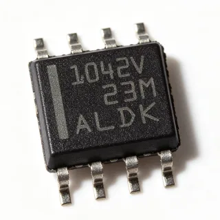
The device is specified for a 3.3 V supply and a -40°C to +85°C operating-temperature range. Its 8-lead SOIC package uses a flow-through pin arrangement intended to simplify PCB layout and signal routing. The LVDS output supports data rates in excess of 600 Mbps, or 300 MHz, making the device suitable for high-speed control links, instrumentation interfaces, backplanes, and embedded communication links.
The current-mode differential output is important for controlling power dissipation and maintaining signal integrity across frequency. The DS90LV027ATM is also designed to minimize short-circuit fault current, which can reduce stress during output faults. Designers should still provide controlled-impedance routing, appropriate return paths, and power-supply decoupling according to the manufacturer’s recommended layout practices.
Typical uses include industrial control systems, high-speed data acquisition, communication equipment, test and measurement instruments, and LVDS links between circuit boards. The dual-driver arrangement is useful when a system needs two high-speed differential outputs but the signal integrity and power requirements favor a dedicated LVDS driver over a general-purpose transceiver.
For PCB implementation, place the device close to the source and destination connectors, keep differential traces paired and symmetric, and use a continuous ground reference beneath the pair. Confirm the receiver’s LVDS input voltage, termination arrangement, cable length, and data-rate requirements before releasing the layout. Request a quote for current availability and lead time through the Request a Quote form on this page.
This page combines manufacturer interface information, drop-in family alternatives, comparison parameters, and practical PCB guidance to support faster component selection and implementation of a reliable LVDS interface.
直接替換替代品,適用於 DS90LV027ATM — 相同封裝,腳位對腳位相容。需重新設計 PCB 的不同封裝零件不列入。
此系列的變體
與下列產品可直接替換的同系列型號: DS90LV027ATM (相同外形與佔位) — 差異在於 Device Type, Operating Temperature Range, Short-Circuit Fault Current.
DS90LV027A
✅ 直接替換📋 參考替代品(不在目錄中)
DS90LV027ATM/NOPB
✅ 直接替換📋 參考替代品(不在目錄中)
DS90LV027ATMX/NOPB
✅ 直接替換📋 參考替代品(不在目錄中)
DS90LV027AQMAX/NOPB
✅ 直接替換📋 參考替代品(不在目錄中)
DS90LV027ATM/NOPB
✅ 直接替換📋 參考替代品(不在目錄中)
DS90LV027ATM 規格
| Device Type | LVDS dual high-speed differential driver |
| Number of Drivers | 2 |
| Technology | CMOS |
| 供應電壓 | 3.3 V |
| Maximum Data Rate | Greater than 600 Mbps |
| Equivalent Clock Rate | 300 MHz |
| Signaling Standard | LVDS |
| Output Architecture | Current-mode differential driver |
| Short-Circuit Fault Current | Minimized |
| 工作溫度範圍 | -40°C to +85°C |
| 封裝 | 8-lead SOIC |
| 安裝類型 | Surface mount |
| PCB Layout | Flow-through pin arrangement |
DS90LV027ATM 8-lead soic 腳位配置指南
DS90LV027ATM(8-lead soic 封裝)的腳位配置。 腳位編號、功能與連接圖定義於製造商資料手冊中。請參閱該手冊以取得確切的封裝尺寸與焊接指引。

無詳細腳位定義資料: DS90LV027ATM.
請參閱 資料表 以查看完整腳位配置。
典型應用
DS90LV027ATM 適用於 6 應用s: Industrial high-speed control links, High-speed instrumentation interfaces, Communication equipment backplanes, High-speed data-acquisition systems, Test and measurement signal distribution, Audio and embedded LVDS interconnects.
Industrial high-speed control links
The DS90LV027ATM fits transmit-only control links between industrial controller boards, remote I/O modules, and data-acquisition equipment. Its dual current-mode LVDS outputs support data rates in excess of 600 Mbps, while the 3.3 V supply and -40°C to +85°C operating range suit embedded industrial environments. The two-channel configuration reduces the number of driver packages when separate differential links are required. Use controlled-impedance routing with a continuous ground reference and terminate each receiver according to its requirements.
推薦
High-speed instrumentation interfaces
DS90LV027ATM can transmit clock, trigger, or control data from an instrumentation system to remote measurement hardware. Supporting more than 600 Mbps, or more than 300 MHz clock rate, provides margin for high-speed sampling and synchronization systems. The current-mode output architecture is designed to limit power dissipation at high frequency, making the device useful where switching noise and thermal load require attention. Keep the differential trace geometry consistent and test the complete cable and receiver path before production.
推薦
Communication equipment backplanes
The DS90LV027ATM is appropriate for point-to-point LVDS links across communication equipment and compact backplanes when two high-speed transmit channels are needed. Its 8-lead SOIC package supports surface-mount assembly, while the flow-through arrangement simplifies signal routing. The 600-Mbps-class capability can carry serialized control, status, or data streams between cards. Designers should verify insertion loss, connector performance, skew, and receiver tolerance across the full operating range.
推薦
High-speed data-acquisition systems
DS90LV027ATM can provide low-power differential transmission for clocks, triggers, and sampled-data control paths in high-speed acquisition equipment. The dual-driver arrangement offers two independent outputs in one 8-SOIC package, while operation above 600 Mbps supports demanding serialized links. The short-circuit fault-current design is beneficial in multi-board systems where output faults must not create excessive stress. Maintain return-path continuity and use receiver-side termination to control reflections.
推薦
Test and measurement signal distribution
The DS90LV027ATM is useful in test and measurement systems that distribute high-speed clocks, triggers, or control commands to remote instrument or DUT connections. Its 3.3 V operation and high data-rate capability allow the same family to support compact, multichannel fixtures. Because the device is a transmitter without an integrated receiver, the destination device must provide compatible LVDS inputs. Validate amplitude, timing margin, cable length, and termination with the complete interconnect rather than relying only on component-level timing.
推薦
Audio and embedded LVDS interconnects
DS90LV027ATM can support high-rate clock distribution and control signaling between embedded audio, control, and processing modules. Two LVDS drivers in an 8-lead SOIC package reduce board-area requirements compared with using two single-channel devices. The current-mode design helps keep dissipation low at elevated data rates, and the 600-Mbps-class capability provides margin for serialized audio control or synchronization paths. Confirm receiver thresholds, termination, and audio-domain timing requirements before integrating the link.
推薦
推薦產品摘要
工程參考資料,適用於 DS90LV027ATM — 比較、設計指引及合規資訊。
選型指南
與替代品比較
| 參數 | 本產品 | DS90LV027A | DS90LV027ATM/NOPB | DS90LV027ATMX/NOPB | DS90LV027AQMAX/NOPB | DS90LV027ATM/NOPB |
|---|---|---|---|---|---|---|
| Package | 8-lead SOIC | 8-lead SOIC | 8-lead SOIC | 8-lead SOIC | 8-lead SOIC | 8-lead SOIC |
| Brand | Texas Instruments | Texas Instruments | Texas Instruments | Texas Instruments | Texas Instruments | Texas Instruments |
| Device Function | Dual LVDS differential driver | Dual LVDS differential driver | Dual LVDS differential driver | Dual LVDS differential driver | Dual LVDS differential driver | Dual LVDS differential driver |
| Number of Drivers | 2 | 2 | 2 | 2 | 2 | 2 |
| Number of Receivers | 0 | 0 | 0 | 0 | 0 | 0 |
| Supply Voltage | 3.3 V | 3.3 V | 3.3 V | 3.3 V | 3.3 V | 3.3 V |
| Data Rate | Greater than 600 Mbps | Greater than 600 Mbps | Greater than 600 Mbps | Greater than 600 Mbps | Greater than 600 Mbps | Greater than 600 Mbps |
| Output Architecture | Current-mode LVDS output | Current-mode LVDS output | Current-mode LVDS output | Current-mode LVDS output | Current-mode LVDS output | Current-mode LVDS output |
主要差異化特點
- Dedicated dual-driver LVDS function (對比DS90LV027A)
- Direct orderable family configuration (對比DS90LV027ATM/NOPB)
- Same-package family sourcing options (對比DS90LV027ATMX/NOPB)
- Qualified family option with same package format (對比DS90LV027AQMAX/NOPB)
設計說明
Route each LVDS differential pair as a tightly coupled, impedance-controlled pair over a continuous ground reference. Keep the driver close to the source connector and receiver, avoid stubs, and maintain symmetric spacing where the board stackup allows. The DS90LV027ATM flow-through arrangement can simplify routing, but connector escape geometry and the receiver location still determine the usable channel length and signal margin.
Use a receiver termination scheme that matches the selected LVDS receiver and system topology. Check input thresholds, differential voltage, and timing margin across the intended temperature and cable conditions. Although the DS90LV027ATM supports data rates in excess of 600 Mbps, the complete link includes the PCB, connector, cable, receiver, and clock source, so each element must be included in the signal-integrity verification.
Place the device power bypass capacitor close to the supply pins and connect the return path directly to the ground plane. The manufacturer describes the current-mode architecture as helping keep power dissipation low at high frequency and minimizing short-circuit fault current. Decouple supply noise locally and review the datasheet power recommendations before adding external filtering that could alter the intended system behavior.
Do not treat DS90LV027A, DS90LV027ATM/NOPB, DS90LV027ATMX/NOPB, and DS90LV027AQMAX/NOPB as identical purchasing codes without checking the orderable suffix, marking, qualification, and production configuration. Also avoid using a generic cross-reference result as proof of drop-in compatibility. Confirm the exact MPN, package, electrical limits, and receiver requirements before approving a substitution.
合規資訊
The manufacturer product page and family product page are the appropriate sources for environmental and qualification documentation; the available product snippets do not state these compliance results.