IP4220CZ6F - Dual USB 2.0 ESD Protection | Nexperia
MPN: IP4220CZ6F ✗ 停產IP4220CZ6F 概覽
The IP4220CZ6 belongs to the ESD-protection and TVS-diode category, where protection components are placed between sensitive connector or interface pins and external cables. Such devices divert transient energy away from downstream circuitry while presenting very low capacitance to high-speed signals. This combination is important because excessive parasitic capacitance can degrade edge rates, reduce signal margin, and impair USB or other high-speed communication links.
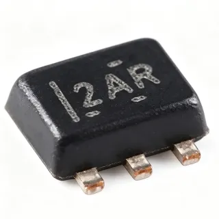
The verified product information identifies four pairs of ultra-low-capacitance protection diodes plus a Zener diode. The Nexperia product page describes the device as suitable for I/O lines sensitive to capacitive load, including USB 2.0, Ethernet, and DVI. The distributor listing identifies IP4220CZ6F as a clamp-type TVS diode in a 6-TSOP surface-mount package. The Mouser result associates the IP4220CZ6 family with the SOT457/SC-74 package and datasheet information.
The manufacturer protection description states ESD protection up to ±8 kV contact, while the supplied search data does not provide a complete set of electrical ratings such as working voltage, leakage current, clamping voltage, capacitance per line, or response time. Those parameters should therefore be confirmed from the official Nexperia datasheet before final circuit release. This page does not infer undocumented values.
Typical applications include USB data-port protection, Ethernet interfaces, DVI connections, and other exposed communication lines where ESD events are expected. Placement close to the connector is generally important because the protection device should intercept transient current before it reaches sensitive logic. PCB routing must preserve the device’s pin-to-channel assignments and provide a low-impedance return path.
When selecting this device, verify the exact channel mapping, package drawing, rated ESD level, signal capacitance, and compatibility with the system’s connector and ground architecture. The available web evidence identifies the component and its intended protection role, but it does not establish lifecycle status, operating-temperature limits, or detailed electrical characteristics. This product data page therefore distinguishes verified facts from parameters requiring datasheet confirmation.
直接替換替代品,適用於 IP4220CZ6F — 相同封裝,腳位對腳位相容。需重新設計 PCB 的不同封裝零件不列入。
IP4220CZ6,125
✅ 直接替換📋 參考替代品(不在目錄中)
IP4220CZ6F 規格
| Product Type | Dual USB 2.0 integrated ESD protection device |
| Protection Structure | Four pairs of ultra-low-capacitance rail-to-rail ESD protection diodes plus a Zener diode |
| ESD Protection Level | Up to ±8 kV contact ESD |
| Nominal ESD System | USB 2.0 |
| Supported Interface Applications | USB 2.0, Ethernet, and Digital Video Interface (DVI) |
| 封裝 | 6-pin SOT457/SC-74 6-TSOP surface-mount package |
| Package Type | Surface Mount |
| 腳位數 | 6 pins |
| Device Classification | Clamp Ipp TVS diode |
| Signal-Line Architecture | Rail-to-rail protection diodes |
IP4220CZ6F surface mount 腳位配置指南
IP4220CZ6F(surface mount 封裝)的腳位配置。 腳位編號、功能與連接圖定義於製造商資料手冊中。請參閱該手冊以取得確切的封裝尺寸與焊接指引。

無詳細腳位定義資料: IP4220CZ6F.
請參閱 資料表 以查看完整腳位配置。
典型應用
IP4220CZ6F 適用於 6 應用s: USB 2.0 Data-Port Protection, Ethernet Interface ESD Protection, DVI Interface Protection, General Exposed I/O Protection, USB-Cross-Linked Peripheral Interfaces, Connector-Centric Robustness Improvement.
USB 2.0 Data-Port Protection
IP4220CZ6F is specifically identified by Nexperia as protection for USB 2.0 I/O lines. Its four pairs of ultra-low-capacitance rail-to-rail ESD diodes are intended to divert electrostatic-discharge transients away from the transceiver and controller while minimizing signal distortion. Place the device near the USB connector or cable-entry point, keep protected traces short, and provide a low-inductance ground return. The verified description specifies ESD protection up to ±8 kV contact, but exact capacitance, working voltage, leakage current, and channel mapping must be confirmed from the official datasheet before release.
推薦
Ethernet Interface ESD Protection
The Nexperia product page lists Ethernet among the interface categories suitable for the IP4220CZ6 protection family. The device can be placed on exposed data or control lines where connector-accessible ESD is a concern. Its rail-to-rail protection architecture provides a defined path for transient current while the ultra-low-capacitance structure helps preserve signal integrity on capacitive-load lines. The application still requires checking line speed, impedance, connector construction, grounding, and the manufacturer’s electrical test conditions. No Ethernet-specific compliance or temperature claims were supplied.
推薦
DVI Interface Protection
IP4220CZ6F is identified by Nexperia as suitable for Digital Video Interface I/O lines sensitive to capacitive loading. The integrated protection network can be positioned at the connector side of a DVI interface to limit ESD energy reaching downstream digital-video circuitry. Because DVI implementations vary in signal count and routing, engineers should map the protected channels from the official pinout and confirm that the added protection capacitance does not compromise edge-rate or impedance requirements. The verified source does not specify DVI-specific ratings beyond the family’s stated protection and low-capacitance characteristics.
推薦
General Exposed I/O Protection
The IP4220CZ6F family is intended for I/O lines exposed to electrostatic discharge, not only USB connectors. It can be evaluated for control, status, or communication lines when the protected signal amplitude and interface topology are compatible with the device’s missing detailed ratings. The four-pair protection arrangement and Zener diode are intended to provide rail-to-rail transient handling, while low capacitance helps reduce loading on sensitive digital lines. Validate the exact working and clamping voltages, leakage, and channel assignments against the datasheet before using it outside the manufacturer’s stated USB, Ethernet, and DVI examples.
推薦
USB-Cross-Linked Peripheral Interfaces
Although the verified manufacturer description names USB 2.0, Ethernet, and DVI, it also describes the device as suitable for I/O lines sensitive to capacitive load. This makes the protection concept potentially useful at peripheral interface entry points where a connector exposes multiple digital lines. The engineer must confirm that each protected line’s voltage and signal integrity requirements are compatible, and that the device’s package and pin mapping match the PCB. The ±8 kV contact ESD figure is a family-level verified claim; it should not be interpreted as a guarantee for every unlisted interface without application-specific testing.
推薦
Connector-Centric Robustness Improvement
A practical use for IP4220CZ6F is to improve ESD robustness at a connector boundary on an otherwise exposed peripheral or communications board. Placing the protector adjacent to the connector can reduce the distance that a transient must travel through sensitive PCB traces, while the rail-to-rail diode network and Zener provide the intended clamping structure. This approach requires careful ground-return routing and verification that protection capacitance does not alter the target interface. The supplied data does not provide a qualified temperature range, so industrial or automotive use requires separate manufacturer confirmation.
推薦
推薦產品摘要
工程參考資料,適用於 IP4220CZ6F — 比較、設計指引及合規資訊。
選型指南
與替代品比較
| 參數 | 本產品 | IP4220CZ6,125 |
|---|---|---|
| Package | SOT457/SC-74 6-pin surface-mount package | SOT457/SC-74 6-pin surface-mount package; provisional same-package candidate |
| Brand | Nexperia | Nexperia |
| Function | Dual USB 2.0 integrated ESD protection | Dual USB 2.0 integrated ESD protection family variant |
主要差異化特點
- Purpose-built dual USB 2.0 protection (對比IP4220CZ6,125)
- Rail-to-rail protection structure (對比IP4220CZ6,125)
- Connector-side application targeting (對比IP4220CZ6,125)
設計說明
Place IP4220CZ6F as close as practical to the connector pins that are exposed to user contact or cable transients. Keep the protected traces short and route the transient return directly to the relevant ground or protection reference. Verify the official six-pin pinout and channel mapping before routing; the supplied search data identifies the package but does not enumerate pin names.
Use the manufacturer’s capacitance test value to check signal-integrity impact for USB 2.0, Ethernet, or DVI. The verified source describes ultra-low capacitance but provides no numerical value, so do not substitute a guessed value. Confirm impedance, edge-rate, channel loading, and connector capacitance in the final interface design.
Do not treat the ±8 kV contact ESD statement as a complete set of device ratings. Working voltage, leakage current, clamping voltage, response time, and temperature limits were not present in the supplied data. Confirm those parameters and the package orientation in the official Nexperia datasheet before production release.
ESD protection is most effective when the transient current has a short, low-inductance path. Avoid long loops between the protected connector lines and the device or its ground reference. Review the placement against the connector mechanical design and keep unrelated high-current or switching paths away from the protected signal region.
合規資訊
The supplied verified data does not state RoHS, REACH, AEC-Q100, lead-free, halogen-free, or conflict-minerals status. Compliance should be confirmed through current Nexperia product and quality documentation.