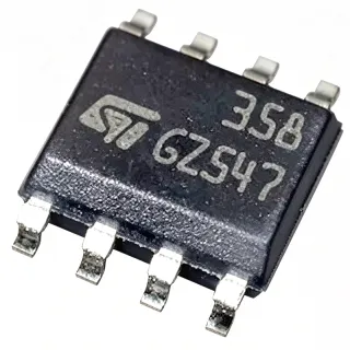
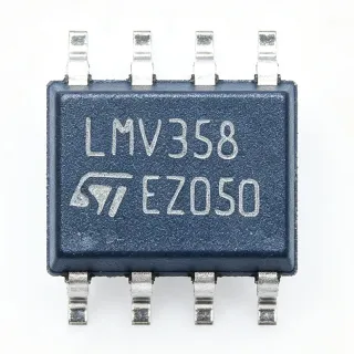
LM358FJ-GE2 - Dual Ground-Sense Op Amp, 36V | ROHM
MPN: LM358FJ-GE2 ✗ 停產LM358FJ-GE2 概覽
An operational amplifier is an analog signal-conditioning semiconductor that uses high open-loop gain to amplify voltage differences while presenting high input impedance and low output impedance. The LM358FJ belongs to the dual operational-amplifier family, combining two amplifier channels in one package. Its ground-sense architecture is intended for measurements referenced to ground, including current-shunt monitoring and low-side sensing.
The principal features are a wide single-supply operating range, low current consumption, ground-capable input and output operation, and two independent amplifiers. The 0.3 V/us slew rate favors general-purpose signal paths rather than demanding high-speed applications. A common-mode rejection ratio of 80 dB helps reject equal-magnitude noise appearing on both inputs, while the maximum input offset voltage of 5,000 uV defines a relatively coarse accuracy class compared with precision amplifier families.
The LM358FJ uses a practical bipolar-style general-purpose amplifier architecture associated with the LM358 product family. Its broad supply tolerance allows operation from low-voltage single-supply systems through industrial rails approaching the 36 V maximum. Because the device is not rail-to-rail at all operating conditions, the usable input and output range must be checked against the selected supply voltage and common-mode requirements.
Typical uses include low-side current monitoring, power-supply feedback, sensor interfaces, battery-current measurement, and general analog signal conditioning. The dual configuration can implement two related channels or provide a differential amplifier and voltage follower within one package. Each channel should be configured for stable operation with the feedback network and compensation values specified by the manufacturer.
Designers should verify input common-mode range, output swing, input bias current, noise behavior, and channel matching against the actual supply. Input and output nodes must remain within their absolute maximum ratings, and unused inputs require an appropriate bias to prevent saturation. PCB placement should keep feedback paths short and provide a stable ground reference close to the amplifier.
This page organizes the manufacturer specifications, lifecycle notice, package information, functional alternatives, application guidance, and engineering checks into a practical design reference. It also identifies where replacement qualification must be confirmed at the pin, electrical, and application level rather than relying only on the generic LM358 family name.
直接替換替代品,適用於 LM358FJ-GE2 — 相同封裝,腳位對腳位相容。需重新設計 PCB 的不同封裝零件不列入。
此產品無可直接替換的替代品。
申請替代品LM358FJ-GE2 最大額定值與電氣特性
| Amplifier Type | Dual general-purpose operational amplifier |
| Number of Amplifier Circuits | 2 circuits |
| Operating Supply Range, Single Supply | 3 V to 32 V |
| Maximum Supply Voltage | 36 V |
| Nominal Supply Voltage | 5 V |
| Input Offset Voltage | Up to 5,000 uV |
| Slew Rate | 0.3 V/us |
| Common-Mode Rejection Ratio | 80 dB |
| 工作溫度範圍 | -40°C to +85°C |
| Temperature Grade | Industrial |
| Input and Output Common-Mode Capability | Ground sense |
| 封裝 | 8-pin SOP-J |
| 安裝類型 | Surface mount |
| Lifecycle Recommendation | Not Recommended for New Designs |
LM358FJ-GE2 腳位配置
| 腳位 1 | OUT1 — Output of amplifier 1 |
| 腳位 2 | IN1- — Inverting input of amplifier 1 |
| 腳位 3 | IN1+ — Non-inverting input of amplifier 1 |
| 腳位 4 | GND — Ground connection |
| 腳位 5 | IN2+ — Non-inverting input of amplifier 2 |
| 腳位 6 | IN2- — Inverting input of amplifier 2 |
| 腳位 7 | OUT2 — Output of amplifier 2 |
| 腳位 8 | VCC — Positive supply connection |
典型應用
LM358FJ-GE2 適用於 6 應用s: Low-Side Shunt Current Monitoring, Battery Current and Charge Monitoring, Power-Supply Feedback and Fault Detection, Industrial Sensor Signal Conditioning, Audio and Communication Interface Buffers, Automotive and Mobile Equipment Ground Interfaces.
Low-Side Shunt Current Monitoring
The LM358FJ-GE2 fits low-side shunt monitoring because its ground-sense input and output architecture is intended to measure small differential voltages near the lower supply rail. A 0.3 V/us slew rate is suitable for typical current-loop bandwidths, and 80 dB common-mode rejection helps reduce disturbance common to both shunt inputs. In the circuit, the shunt converts current into a differential millivolt-level signal and the amplifier applies the required gain. Designers should include the up-to-5,000 uV input offset in the measurement error, confirm the input common-mode range at the actual supply voltage, and verify output headroom before scaling the current range.
推薦
Battery Current and Charge Monitoring
The LM358FJ-GE2 can amplify voltage across a ground-side battery-current sensor when the design operates from a single supply. Its 3 V to 32 V operating range permits use in systems supplied by low-voltage cells through higher industrial rails, while the ground-sense behavior supports measurements whose voltage approaches ground. The amplifier would typically sit between the shunt and an ADC input, with filtering added for switching noise. Critical checks include shunt common-mode voltage, input bias-current error, offset voltage, ADC input range, and battery disconnect transients. The device's not-for-new-design status makes lifecycle approval essential for new battery-management equipment.
推薦
Power-Supply Feedback and Fault Detection
The LM358FJ-GE2 is appropriate for power-supply feedback, fault comparison, and slow supervisory functions that require a dual amplifier in a surface-mount package. Its 36 V maximum supply voltage supports applications above conventional low-voltage logic rails, and the 0.3 V/us slew rate is adequate for many error amplifiers and threshold detectors. In a feedback network, the closed-loop behavior depends on the feedback network and compensation rather than slew rate alone. Engineering review should cover output saturation during startup, input offset, capacitive loading, and the tolerance of external threshold components. Use the manufacturer's recommended compensation and output-capacitance limits to avoid instability.
推薦
Industrial Sensor Signal Conditioning
The LM358FJ-GE2 can condition outputs from slow industrial sensors when the required bandwidth and accuracy are consistent with a general-purpose dual amplifier. The wide 3 V to 32 V single-supply range simplifies interface design across mixed industrial systems, while 80 dB common-mode rejection improves immunity to noise appearing equally on both sensor inputs. A practical implementation buffers the sensor, applies gain, and filters noise before an ADC or controller input. The input common-mode range and output swing must be evaluated at the lowest and highest supply conditions. Because offset voltage can reach 5,000 uV, systems requiring calibrated high accuracy should account for that error or use a precision amplifier instead.
推薦
Audio and Communication Interface Buffers
The dual LM358FJ-GE2 can provide inexpensive buffering and gain for low-frequency audio or communications interfaces when the application does not require rail-to-rail swing or high slew rate. The 0.3 V/us slew rate supports many voice-band and control signals, and the dual channel can implement matching gain stages. Each channel should use feedback selected for stable operation, and the output must remain inside the voltage range allowed by the chosen supply. Designers should also evaluate input offset, bias current, capacitive loading, and channel-to-channel matching. For line-level audio, distortion and noise requirements should be checked against the complete circuit rather than inferred from slew rate alone.
推薦
Automotive and Mobile Equipment Ground Interfaces
The LM358FJ-GE2 is technically suited to ground-referenced signal interfaces because it supports a broad single-supply range and ground-sense operation. The wide supply ceiling of 36 V is useful for industrial and vehicle electrical environments, although transient protection and absolute-maximum limits still require separate review. The amplifier can buffer sensor lines, monitor return-path currents, or amplify small differential signals referenced to ground. Because this exact product is not recommended for new designs, an automotive or mobile program should obtain lifecycle approval or choose a currently supported amplifier family. Validate ISO 7637-2, ISO 16750, or other applicable transient requirements independently rather than assuming amplifier compliance.
推薦
推薦產品摘要
工程參考資料,適用於 LM358FJ-GE2 — 比較、設計指引及合規資訊。
選型指南
與替代品比較
| 參數 | 本產品 |
|---|---|
| Package | 8-pin SOP-J |
| Brand | ROHM Semiconductor |
| Amplifier Configuration | Dual |
| Operating Supply Range | 3 V to 32 V |
| Maximum Supply Voltage | 36 V |
| Nominal Supply Voltage | 5 V |
| Input Offset Voltage | Up to 5,000 uV |
| Slew Rate | 0.3 V/us |
| Common-Mode Rejection Ratio | 80 dB |
| Operating Temperature Range | -40°C to +85°C |
| Ground-Sense Operation | Supported |
| Lifecycle Recommendation | Not Recommended for New Designs |
主要差異化特點
- Ground-sense architecture (對比LM2904)
- Wide single-supply operating range (對比LM358N)
- Defined industrial temperature grade (對比Consumer-grade LM358 variants)
設計說明
Do not treat every LM358-family device as a footprint-compatible substitute for LM358FJ-GE2. Confirm the 8-pin SOP-J land pattern, numbered pin functions, supply range, input common-mode range, output swing, offset voltage, slew rate, and stability requirements. A generic LM358 name or similar input offset specification is not evidence of pin-to-pin compatibility, particularly when the alternative uses SOIC-8 or DIP-8.
Place the amplifier, its input filtering components, and the ground reference close to one another to minimize sensitive-input trace length. Route each non-inverting input away from output and supply-current paths. Use a low-impedance ground plane, decouple the supply near the device, and keep the feedback loop compact. For shunt measurements, connect the amplifier ground directly to the appropriate ground-sensing point to reduce voltage drops and shared copper noise.
The 0.3 V/us slew rate limits large-signal response, so account for it when setting closed-loop bandwidth and slew-triggered error. Also budget the input offset of up to 5,000 uV, amplifier input-bias error, shunt tolerance, and ADC error. For small differential signals, an instrumentation or precision current-sense amplifier may provide better accuracy and common-mode behavior than a general-purpose dual amplifier.
合規資訊
ROHM identifies LM358FJ-GE2 as not recommended for new designs. Specific environmental, substance, and automotive qualification statements were not identified in the manufacturer product-page summary, so each compliance field remains unknown.