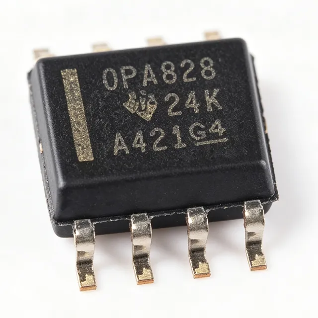
OPA828IDR - 45MHz JFET Op Amp, 4nV/√Hz | TI | Precision Amplifier
MPN: OPA828IDR ✓ 啟用中OPA828IDR 概覽
A JFET-input operational amplifier is a type of precision amplifier whose input stage uses junction field-effect transistors, providing extremely low input bias current (picoampere range) and high input impedance. Within the signal-chain hierarchy, op amps sit between sensors and data converters, serving as the general-purpose analog building block for amplification, filtering, buffering, and transimpedance conversion.
Key features include 50 uV input offset voltage, 0.45 uV/C offset drift, 1 pA typical input bias current, and only 60 nVRMS of noise from 0.1 Hz to 10 Hz. These DC precision specifications make the OPA828 suitable for applications where both speed and accuracy are demanded simultaneously - a rare combination. MUX-friendly inputs allow multiplexed signal chains without settling artifacts or charge-injection damage.
Architecturally, the OPA828 pairs a JFET input stage with a rail-to-rail output stage, combining classic precision topology with modern output swing. The RRO output maximizes dynamic range in low-voltage systems while the 36 V supply rating supports traditional ±15 V industrial analog rails without redesign.
Typical applications include photodiode transimpedance amplifiers (TIA), high-fidelity audio front ends, precision ADC and DAC buffer stages, and active filters in test and measurement instrumentation. The wide 36 V supply range is particularly valuable for industrial designs retaining legacy ±15 V rails.
For design, ensure supply decoupling with 0.1 uF ceramic capacitors placed within 3 mm of each supply pin. When replacing an OPA627, verify compensation and bias-current paths, as community feedback shows some legacy TIA circuits require adjustment despite pin compatibility.
This page synthesizes distributor pricing, drop-in alternatives, and practical design notes not found in the manufacturer datasheet.
直接替換替代品,適用於 OPA828IDR — 相同封裝,腳位對腳位相容。需重新設計 PCB 的不同封裝零件不列入。
此系列的變體
與下列產品可直接替換的同系列型號: OPA828IDR (相同外形與佔位) — 差異在於 Slew Rate, Gain Bandwidth Product, Input Bias Current, Package, Supply Voltage Range.
OPA827AIDR
✅ 直接替換📋 參考替代品(不在目錄中)
OPA827IDR
✅ 直接替換 ⚠️ 規格未經驗證📋 參考替代品(不在目錄中)
OPA627AIDR
✅ 直接替換 ⚠️ 規格未經驗證📋 參考替代品(不在目錄中)
AD8610ARZ
✅ 直接替換📋 參考替代品(不在目錄中)
OPA828IDR 最大額定值與電氣特性
| Amplifier Type | JFET-input operational amplifier |
| Number of Channels | 1 |
| Gain Bandwidth Product | 45 MHz |
| Slew Rate | 150 V/us |
| Input Voltage Noise Density | 4 nV/√Hz at 1 kHz |
| Input Voltage Noise (0.1 Hz to 10 Hz) | 60 nVRMS |
| Input Bias Current | 1 pA (typical) |
| Input Offset Voltage | 50 uV |
| Input Offset Voltage Drift | 0.45 uV/C |
| Supply Voltage Range | ±4 V to ±18 V (36 V total) |
| 輸出類型 | Rail-to-rail output (RRO) |
| Input Type | MUX-friendly JFET inputs |
| 封裝 | 8-SOIC (SO-8) |
| 安裝類型 | Surface Mount |
| Predecessor Parts | OPA627, OPA827 |
OPA828IDR 腳位配置
| 腳位 1 | NC — Not connected (per datasheet) |
| 腳位 2 | IN- — Inverting input |
| 腳位 3 | IN+ — Non-inverting input |
| 腳位 4 | V- — Negative supply |
| 腳位 5 | NC — Not connected (per datasheet) |
| 腳位 6 | OUT — Rail-to-rail output |
| 腳位 7 | V+ — Positive supply |
| 腳位 8 | NC — Not connected (per datasheet) |
典型應用
OPA828IDR 適用於 6 應用s: Photodiode Transimpedance Amplifier, High-Fidelity Audio Front End, Precision ADC/DAC Buffering, Test and Measurement Instrumentation, Industrial ±15 V Analog Signal Chains, Sensor Signal Conditioning and Active Filters.
Photodiode Transimpedance Amplifier
The OPA828IDR's 1 pA typical input bias current and 50 uV offset voltage make it a strong fit for photodiode transimpedance amplifiers, where input current error directly translates to measurement offset at the photodiode's high source impedance. The 45 MHz gain bandwidth supports large feedback resistors with fast photodiode signals, while 4 nV/√Hz voltage noise keeps amplifier voltage noise contribution manageable when referred through high-value feedback resistors. MUX-friendly inputs tolerate multiplexed photodiode arrays without charge-injection damage or long settling artifacts. In practice, the TIA feedback capacitor must be sized against the 45 MHz bandwidth for stability; designers migrating from OPA627 circuits should re-verify compensation, as E2E field reports show swapped parts can oscillate without adjustment.
推薦
High-Fidelity Audio Front End
In audio signal chains, the OPA828IDR contributes 60 nVRMS of noise from 0.1 Hz to 10 Hz and 4 nV/√Hz broadband noise, keeping the amplifier below the noise floor of most preceding circuitry, while its JFET inputs present negligible loading to phono cartridges, volume potentiometers, and vacuum-tube stage outputs. The ±18 V maximum supply supports headroom for full-scale line-level and headphone-drive stages on conventional ±15 V rails, and the rail-to-rail output maximizes swing on reduced supply designs. Community comparisons against the OPA627 and OPA827 on diyAudio show competitive measured performance; designers prioritizing absolute lowest low-frequency noise may still prefer the OPA827A grade, trading away the OPA828's double bandwidth and 150 V/us slew rate.
推薦
Precision ADC/DAC Buffering
Driving precision converters demands an amplifier that settles quickly without degrading DC accuracy - exactly the OPA828IDR's combination of 45 MHz bandwidth, 150 V/us slew rate, 50 uV offset, and 0.45 uV/C drift. The rail-to-rail output preserves dynamic range into converter full-scale even on ±5 V or single-supply rails, while the 36 V total rating permits the same buffer design on ±15 V systems. MUX-friendly inputs are specifically valuable in multiplexed data-acquisition front ends, where channel switching imposes charge transients that can damage or disturb non-MUX-tolerant inputs. For switch-capacitor SAR ADC inputs, a small series resistor per TI datasheet guidance isolates the amplifier from converter charge kickback; verify settling to the required ADC resolution within the conversion aperture using the 45 MHz small-signal bandwidth.
推薦
Test and Measurement Instrumentation
Bench instruments, oscilloscope front ends, and automated test equipment benefit from the OPA828IDR's simultaneous speed and precision: 45 MHz of gain bandwidth supports megahertz-range signal paths, while 1 pA bias current and 50 uV offset preserve DC measurement integrity on high-impedance probes and attenuators. The wide ±4 V to ±18 V supply range lets one amplifier design serve both portable battery-powered instruments and benchtop equipment on ±15 V rails, simplifying platform BOMs. Active filter stages in the instrument's signal path also exploit the 150 V/us slew rate for full-scale high-frequency signals without slew-induced distortion. MUX-friendly inputs permit input-channel multiplexing in data loggers and automated test matrices without dedicated protection circuitry at moderate source impedances.
推薦
Industrial ±15 V Analog Signal Chains
Many industrial PLCs, motor-control supervisory circuits, and process instrumentation still run on legacy ±15 V analog rails. The OPA828IDR's ±18 V maximum supply rating accepts these rails directly with margin, eliminating the need for local point-of-load regulation when upgrading aging op amp sockets. Its rail-to-rail output stage extracts maximum signal swing from the ±15 V rails, improving measurement resolution into downstream ADCs, and the 36 V total supply rating tolerates industrial supply transients better than lower-voltage precision amplifiers. The 0.45 uV/C offset drift maintains calibration accuracy across factory-floor temperature swings, while the 4 nV/√Hz noise keeps small transducer signals, such as strain-gauge bridge outputs after pre-amplification, cleanly above the amplifier noise floor.
推薦
Sensor Signal Conditioning and Active Filters
High-impedance sensors - piezoelectric accelerometers, hydrophones, pH electrodes via buffer stages, and infrared detectors - require amplifiers whose input bias current does not swamp the signal. The OPA828IDR's 1 pA bias current and high JFET input impedance preserve accuracy at these source impedances, while 45 MHz bandwidth supports active filter topologies such as multiple-feedback and Sallen-Key designs operating into the hundreds of kilohertz. The 150 V/us slew rate ensures large-signal filter stages do not slew-limit, keeping harmonic distortion low at full-scale outputs. In active filter applications, the wide ±18 V supply range increases filter headroom and reduces distortion for a given output level, and the RRO stage supports low-voltage versions of the same filter design for portable instruments.
推薦
推薦產品摘要
工程參考資料,適用於 OPA828IDR — 比較、設計指引及合規資訊。
選型指南
與替代品比較
| 參數 | 本產品 | OPA827AIDR | OPA827IDR | OPA627AIDR | AD8610ARZ |
|---|---|---|---|---|---|
| Package | 8-SOIC | 8-SOIC - same | 8-SOIC - same | 8-SOIC - same | 8-SOIC - same |
| Brand | Texas Instruments | Texas Instruments | Texas Instruments | Texas Instruments | Analog Devices |
| Gain Bandwidth | 45 MHz | ~22 MHz | ~22 MHz | ~16 MHz | ~25 MHz |
| Slew Rate | 150 V/us | ~22 V/us | ~22 V/us | ~55 V/us | ~42 V/us |
| Input Voltage Noise | 4 nV/√Hz at 1 kHz | ~3.8 nV/√Hz | ~3.8 nV/√Hz | ~4.5 nV/√Hz | ~6 nV/√Hz |
| Input Bias Current | 1 pA typical | pA class (JFET) | pA class (JFET) | pA class (JFET) | pA class (JFET) |
| Maximum Supply Voltage | 36 V total (±18 V) | ~40 V total | ~40 V total | ~36 V total | ~26 V total (±13 V) |
| Output Stage | Rail-to-rail output (RRO) | Non-RRO | Non-RRO | Non-RRO | Rail-to-rail output |
主要差異化特點
- Double the bandwidth of its predecessor family (對比OPA827AIDR)
- Dramatic cost reduction vs OPA627 (對比OPA627AIDR)
- Rail-to-rail output on 36 V supply (對比OPA827AIDR)
- Wider supply headroom than closest ADI equivalent (對比AD8610ARZ)
設計說明
Place 0.1 uF ceramic decoupling capacitors within 3 mm of each supply pin (V+ pin 7, V- pin 4), with a shared 2.2-10 uF bulk capacitor per supply rail. The OPA828's 45 MHz bandwidth makes it sensitive to supply inductance; long decoupling traces can create high-frequency instability. Follow the TI datasheet PCB layout guidance and use a solid ground plane under the amplifier area. Keep feedback paths short and avoid routing high-impedance input traces (pins 2, 3) near switching signals to protect the picoampere-class bias-current performance from leakage and capacitive pickup.
Although TI lists the OPA828 as a drop-in replacement for the OPA627, E2E forum reports document cases where swapping the part in legacy photodiode TIA circuits produced no output until compensation was reworked. Before direct substitution, verify the feedback network stability margin with the OPA828's 45 MHz bandwidth (roughly 2x the OPA827), check any compensation capacitor values, and confirm bias-current return paths. Also note the OPA627 SOIC package offered pin-strapping options some legacy boards exploited - compare the pin functions on your specific PCB rather than assuming socket equivalence.
The OPA828IDR accepts ±4 V to ±18 V (36 V total). On ±15 V rails, verify total supply stays below 36 V including transients - industrial rails can drift high during unloaded conditions. For single-supply operation, the rail-to-rail output swings close to the negative rail but the JFET input common-mode range does not include the negative rail; keep input common-mode within the datasheet-specified range above V-. Estimated: a 45 MHz amplifier driving a 10 Vpp load at 500 kHz requires 15.7 V/us slew rate, comfortably inside the 150 V/us rating, confirming ample large-signal margin for typical buffer duties.
合規資訊
Compliance certificates should be obtained from the TI product folder for the exact orderable part; retrieved web data did not include explicit RoHS/REACH statements.







