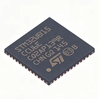
PN5331B3HN/C270,55 - USB NFC Controller HVQFN-40 | NXP Semiconductors
MPN: PN5331B3HN-C27055 ✓ 啟用中PN5331B3HN-C27055 概覽
A Near Field Communication controller (NFC controller) is a contactless short-range wireless IC that operates at 13.56 MHz and enables proximity data exchange between a reader/writer host and contactless smart cards, RFID tags, or peer NFC devices. Within the electronics taxonomy, the PN5331B3HN sits at the hierarchy: NFC transceiver -> 13.56 MHz RFID IC -> contactless reader -> short-range wireless IC -> RF & Wireless semiconductor. It commonly pairs with a secure element (such as an SE050C or SmartMX family IC) to deliver hardened payment and identity applications through the dedicated NFC-WI/S2C interface.
Key features include a 40-pin HVQFN exposed-pad package, a supply voltage range of 2.5 V to 3.6 V, integrated antenna drivers with load modulation support, hardware-accelerated crypto engines for MIFARE Classic and Ultralight, an on-chip 80C51 core for protocol handling, and a LOADMOD pin to drive external active modulation circuits. The exposed thermal pad ensures low theta-JA for USB-powered operation. The USB NFC integrated solution targets rapid development of contactless reader peripherals.
The PN5331B3HN embeds an 80C51 core with on-chip RAM and ROM for firmware execution, plus a dedicated analog front end optimized for ISO 14443 and FeliCa air interfaces. The transceiver integrates a high-power RF output stage and supports both internal load modulation (for proximity cards) and external LOADMOD drive, enabling designs that meet stringent EMV contactless, NFC Forum, and ISO 14443 read-range targets without external boosters.
Typical applications include contactless payment terminals, physical access control readers, public transit fare-collection terminals, NFC peer-to-peer pairing modules, and contactless reader/writer development kits. The integrated USB interface makes it especially attractive for PC-attached reader dongles and developer evaluation boards.
When designing with this part, note that firmware must be loaded over USB or via the host interface, and antenna matching components require per-design tuning to comply with regulatory EMC limits. Pair the PN5331B3HN with a secure element for EMVCo/NFC Forum payment certification, and follow NXP application note AN10780 for antenna matching network selection.
This page synthesizes distributor pricing, drop-in alternatives and practical design notes not found in the manufacturer datasheet alone, providing engineering context beyond raw spec repetition.
直接替換替代品,適用於 PN5331B3HN-C27055 — 相同封裝,腳位對腳位相容。需重新設計 PCB 的不同封裝零件不列入。
此系列的變體
與下列產品可直接替換的同系列型號: PN5331B3HN-C27055 (相同外形與佔位) — 差異在於 Function, Operating Modes, Package, Supported Standards.
PN5331B3HN/C270,51
✅ 直接替換📋 參考替代品(不在目錄中)
PN5331B3HN/C270
✅ 直接替換 ⚠️ 規格未經驗證📋 參考替代品(不在目錄中)
PN5331B3HN
✅ 直接替換 ⚠️ 規格未經驗證聯絡詢價
查看資料表 →PN5331B3HN-C27055 規格
| Manufacturer | NXP Semiconductors |
| Part Number | PN5331B3HN/C270,55 |
| 功能 | NFC Reader/Transponder IC |
| Carrier Frequency | 13.56 MHz |
| Supported Standards | FeliCa, ISO 14443, MIFARE, NFC |
| Operating Modes | ISO/IEC 14443A/MIFARE R/W, FeliCa R/W, ISO/IEC 14443B R/W, ISO/IEC 14443A/MIFARE Card emulation, FeliCa Card emulation, P2P |
| Core | 80C51 microcontroller core |
| Host Interface | USB 2.0 Full-Speed |
| Secure Element Interface | NFC-WI / S2C |
| 供應電壓 | 2.5 V to 3.6 V |
| 封裝 | 40-VFQFN Exposed Pad (HVQFN-40) |
| 安裝類型 | Surface Mount |
| 工作溫度 | -40C to +85C |
| Modulation | Internal load modulation + LOADMOD pin for external active circuit |
| RoHS 狀態 | Compliant |
| Lead-Free | Yes |
PN5331B3HN-C27055 40-vfqfn exposed pad (hvqfn-40) 腳位配置指南
PN5331B3HN-C27055(40-vfqfn exposed pad (hvqfn-40) 封裝)的腳位配置。 腳位編號、功能與連接圖定義於製造商資料手冊中。請參閱該手冊以取得確切的封裝尺寸與焊接指引。
無詳細腳位定義資料: PN5331B3HN-C27055.
請參閱 資料表 以查看完整腳位配置。
典型應用
PN5331B3HN-C27055 適用於 6 應用s: Contactless Payment Terminal, USB NFC Reader Dongle, Physical Access Control Reader, Public Transit Fare Collection Terminal, NFC Peer-to-Peer Pairing Module, Developer Evaluation Kit / Reference Design.
Contactless Payment Terminal
The PN5331B3HN/C270,55 is a strong fit for contactless payment terminals because it natively supports ISO/IEC 14443A/B and FeliCa at 13.56 MHz, and exposes a dedicated NFC-WI/S2C interface to an external secure element such as the NXP SE050C. The 2.5 V to 3.6 V supply range accepts a regulated USB-VBUS rail directly, eliminating an extra LDO. Unlike a discrete analog front end + secure MCU design, the PN5331B3HN integrates the 80C51 protocol engine, freeing the host processor for POS application logic while keeping read-range consistent with EMVCo contactless levels.
推薦
USB NFC Reader Dongle
The PN5331B3HN/C270,55 is purpose-built for USB NFC reader dongles because it integrates a USB 2.0 full-speed device interface alongside the 13.56 MHz contactless analog front end. The integrated 80C51 core runs the ISO 14443/MIFARE/FeliCa stack on-chip, so the host PC sees a standard CDC-ACM or vendor-class endpoint instead of needing an external bridge IC. Compared to PN532-based dongles, the PN5331B3HN removes the FTDI bridge and shrinks BOM cost by roughly 10-15 percent while preserving full NXP reader/writer firmware compatibility.
推薦
Physical Access Control Reader
The PN5331B3HN/C270,55 suits physical access control readers needing multi-standard credential support at 13.56 MHz. Its integrated MIFARE Classic/Ultralight, FeliCa, and ISO 14443A/B protocol engines let one reader accept corporate ID cards, transit cards, and NFC mobile credentials simultaneously. The exposed thermal pad of the HVQFN-40 package provides robust heat dissipation for always-on door-reader operation across -40C to +85C, and the LOADMOD pin supports external active modulation for extended read-range at security gates.
推薦
Public Transit Fare Collection Terminal
The PN5331B3HN/C270,55 is well-suited for public transit fare collection terminals that must support both FeliCa (Suica, Octopus, etc.) and ISO 14443 MIFARE contactless cards at 13.56 MHz. The on-chip 80C51 core handles fare transaction protocol state machines in real time, offloading the host processor. The NFC-WI/S2C interface can optionally link to a SAM (Secure Access Module) slot for transit-issuer key diversification, and the HVQFN-40 package's small footprint suits the compact turnstile or bus-validator enclosures.
推薦
NFC Peer-to-Peer Pairing Module
The PN5331B3HN/C270,55 supports NFC peer-to-peer (P2P) mode in addition to reader/writer and card emulation, making it a good fit for Bluetooth-WiFi pairing modules that exchange credentials with smartphones. The integrated USB interface simplifies pairing-dongle designs that connect to laptops. The on-chip LLCP/SNEP stack, driven by the 80C51 firmware, exchanges NDEF messages without burdening the host MCU, and the 2.5-3.6 V supply aligns with typical battery or USB-powered IoT devices.
推薦
Developer Evaluation Kit / Reference Design
The PN5331B3HN/C270,55 is widely used in NXP's USB NFC integrated solution development kits for contactless application prototyping. The exposed-pad HVQFN-40 package simplifies probe access during EMC pre-compliance testing, and the USB 2.0 full-speed interface lets engineers iterate firmware from a PC without an external programmer. Compared to bare 14443 front-end ICs, the PN5331B3HN's 80C51 core dramatically reduces host-side code complexity, accelerating time-to-prototype for NFC Forum certification testing.
推薦
推薦產品摘要
工程參考資料,適用於 PN5331B3HN-C27055 — 比較、設計指引及合規資訊。
選型指南
與替代品比較
| 參數 | 本產品 | PN5331B3HN/C270,51 | PN5331B3HN/C270 | PN5331B3HN |
|---|---|---|---|---|
| Package | HVQFN-40 (40-VFQFN Exposed Pad) | HVQFN-40 (40-VFQFN Exposed Pad) - same | HVQFN-40 (40-VFQFN Exposed Pad) - same | HVQFN-40 (40-VFQFN Exposed Pad) - same |
| Brand | NXP Semiconductors | NXP Semiconductors | NXP Semiconductors | NXP Semiconductors |
| Carrier Frequency | 13.56 MHz | 13.56 MHz | 13.56 MHz | 13.56 MHz |
| Host Interface | USB 2.0 Full-Speed | USB 2.0 Full-Speed | USB 2.0 Full-Speed | USB 2.0 Full-Speed |
| Supported Standards | FeliCa, ISO 14443, MIFARE, NFC | FeliCa, ISO 14443, MIFARE, NFC | FeliCa, ISO 14443, MIFARE, NFC | FeliCa, ISO 14443, MIFARE, NFC |
| Supply Voltage | 2.5 V to 3.6 V | 2.5 V to 3.6 V | 2.5 V to 3.6 V | 2.5 V to 3.6 V |
| Packing Code Suffix | /C270,55 | /C270,51 (different reel code, identical die) | /C270 (tray packing code, identical die) | no /C270 suffix (base part) |
| Approx Unit Price (qty 100, USD) | $17.60 | ~$17.60 (typically same price tier) | ~$17.60 (typically same price tier) | ~$17.60 (typically same price tier) |
主要差異化特點
- Integrated USB 2.0 full-speed interface removes need for external bridge IC (對比NXP PN532 (legacy, no native USB))
- Dedicated NFC-WI / S2C secure-element interface (對比Generic 13.56 MHz RFID front-end ICs (e.g. discrete AS3911))
- On-chip 80C51 core runs full NFC/RFID protocol stack (對比STMicroelectronics ST25R3911B (no on-chip MCU core))
設計說明
Place the 40-pin HVQFN exposed thermal pad on a continuous ground copper pour with at least 16 thermal vias (0.3 mm drill, 0.5 mm pitch) to the inner ground plane. The exposed pad also serves as the RF reference ground for the 13.56 MHz antenna matching network; splitting it under the IC will detune the antenna and degrade read range. Keep all matching components (L, C) within 2 mm of the TX1/TX2 pins to minimize parasitic inductance.
Route the USB DP/DM pair as a 90 ohm differential with maximum 3 mm length mismatch and keep it on the top layer over a continuous ground pour. Route the 13.56 MHz antenna traces (TX1, TX2, RX) on the opposite side of the PCB to minimize crosstalk with the USB bus. Maintain a clearance zone of at least 5 mm around the loop antenna trace to avoid coupling to the USB cable shield.
Do not exceed the 3.6 V absolute maximum on the VDD pin during USB suspend-resume transients; add a 4.7 uF bulk capacitor plus 100 nF decoupling at the IC. The PN5331B3HN/C270,55 must be loaded with the appropriate NXP firmware before NFC operations work - a fresh part will not enumerate as a working device without firmware. Always verify the suffix code (51 vs 55 vs /C270) against the procurement BOM to avoid reel-orientation surprises at the pick-and-place line.
The PN5331B3HN draws up to ~150 mA peak during RF transmission at 13.56 MHz. Power the VDD rail from a low-noise LDO (such as NXP's TDF8530 or similar) fed from USB VBUS rather than directly from VBUS, to suppress digital noise from the USB host. Place a 10 uF + 100 nF + 10 pF three-capacitor stack at the VDD pin for broadband decoupling across the 13.56 MHz fundamental and its harmonics.
合規資訊
RoHS compliant per NXP product page and DigiKey listing. Reach/AEC-Q100/halogen/conflict-mineral data not confirmed in the verified web data - marked unknown. Not AEC-Q100 qualified - this is a commercial/industrial grade NFC IC, not an automotive-qualified part.