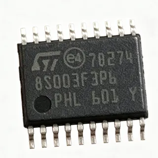
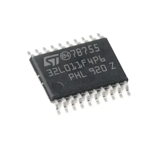
STM8S903F3P6 - 16MHz 8-Bit MCU | STMicroelectronics
MPN: STM8S903F3P6 ✓ 啟用中STM8S903F3P6 概覽
An 8-bit microcontroller is a programmable semiconductor containing a processor core, nonvolatile program memory, data memory, and integrated peripherals. Within the hierarchy of embedded semiconductors, an MCU is below a microprocessor in processing capability but combines greater control simplicity with lower system cost and power use. The STM8S903F3 belongs to STMicroelectronics’ STM8S access line and targets cost-sensitive consumer, appliance, and industrial-control applications.
Key features include 8 KB of Flash, 1 KB of RAM, and 640 bytes of EEPROM, allowing firmware, working data, and nonvolatile parameters to be consolidated in one device. The 10-bit ADC supports analog measurement, while two timers support timing and periodic control functions. UART, SPI, and I²C interfaces cover serial communication, sensor connectivity, and expansion to external ICs. The 2.95 V to 5.5 V supply range accommodates both 3.3 V and 5 V system environments.
The STM8S903F3 architecture combines an 8-bit STM8 core with dedicated peripheral resources and true data EEPROM. Its 16 MHz maximum clock rate provides sufficient processing bandwidth for control loops, user-interface scanning, communications, and low-complexity signal processing. At the same time, the 20-TSSOP package limits board footprint, making it practical for compact embedded products. Detailed pin-level functions and electrical limits should be confirmed against the manufacturer datasheet before layout release.
Typical uses include appliance control, small industrial controllers, digital input and output modules, sensor interfaces, compact timers, and embedded communication nodes. The STM8S903F3P6 is particularly suitable when a design requires several serial interfaces alongside analog sensing but does not justify the software complexity or cost of a 32-bit MCU. Its integrated EEPROM is useful for retaining configuration data, calibration values, or counters without an external memory component.
Designers should confirm the exact 20-TSSOP land pattern, pin multiplexing, oscillator connections, reset implementation, and peripheral pin assignments using the official datasheet. Decoupling and signal-integrity layout should follow the manufacturer recommendations, while software validation should include startup, clock configuration, ADC accuracy, timer behavior, and communications under expected bus loading. The broad 2.95 V to 5.5 V range does not remove the need to verify every peripheral and I/O condition at the minimum and maximum system voltages.
直接替換替代品,適用於 STM8S903F3P6 — 相同封裝,腳位對腳位相容。需重新設計 PCB 的不同封裝零件不列入。
此系列的變體
與下列產品可直接替換的同系列型號: STM8S903F3P6 (相同外形與佔位) — 差異在於 ADC Resolution, Communication Interfaces, Core, Data EEPROM, Operating Temperature.
STM8S103F3P6
✅ 直接替換聯絡詢價
查看資料表 →STM8S903F3P6 最大額定值與電氣特性
| Microcontroller Type | 8-bit STM8S microcontroller |
| Maximum Clock Speed | 16 MHz |
| Flash Program Memory | 8 KB |
| RAM | 1 KB |
| EEPROM | 640 bytes |
| Supply Voltage Range | 2.95 V to 5.5 V |
| ADC Resolution | 10 bits |
| Timer Count | 2 timers |
| Serial Interfaces | UART, SPI, and I²C |
| I/O Port Count | 16 |
| 封裝 | 20-TSSOP |
| Package Width | 4.40 mm |
| Package Pitch | 0.65 mm |
| 安裝類型 | Surface Mount |
| 生命週期狀態 | Active |
| RoHS Compliance | Compliant |
| Architecture | 8-bit CISC |
| Programming Memory Type | Flash |
STM8S903F3P6 0.65 mm 腳位配置指南
STM8S903F3P6(0.65 mm 封裝)的腳位配置。 此數位 IC 包含 GPIO、通訊介面(UART、SPI、I2C)與電源腳位。替代腳位功能與配置選項請參閱製造商資料表。對嵌入式系統設計與 PCB 佈局至關重要。

無詳細腳位定義資料: STM8S903F3P6.
請參閱 資料表 以查看完整腳位配置。
典型應用
STM8S903F3P6 適用於 6 應用s: Appliance Control Module, Industrial Sensor Interface, Digital I/O and Relay Control, Embedded Communication Node, Compact Timer and Sequencer, Low-Cost Consumer Controller.
Appliance Control Module
The STM8S903F3P6 fits compact appliance controllers because its 8-bit STM8S core runs at up to 16 MHz, while 8 KB of Flash stores the control application and 1 KB of RAM supports operating state. The integrated 10-bit ADC can read sensors or potentiometers, the two timers can control motor or switching intervals, and UART, SPI, and I²C support external drivers and user interfaces. Its 2.95 V to 5.5 V supply range accommodates common appliance rails, while the 20-TSSOP package limits PCB area. The 640-byte EEPROM can retain settings, calibration coefficients, or operating counters. Firmware should verify the required timer channels, pin multiplexing, and communication rates against the official datasheet before production.
Industrial Sensor Interface
For an industrial sensor interface, the STM8S903F3P6 combines a 10-bit ADC with three serial communication choices in a compact 20-TSSOP package. It can sample analog sensor inputs, condition the values in software, and forward measurements through UART or I²C to a controller, while SPI can connect to higher-throughput sensors or external data devices. The 8-bit architecture is appropriate for periodic readings, threshold control, status reporting, and local calibration rather than intensive signal processing. Operating from 2.95 V to 5.5 V provides flexibility around 3.3 V and 5 V sensor systems. Because the verified data does not specify ADC accuracy or complete pin assignments, the design must validate input impedance, acquisition timing, noise behavior, and channel availability.
Digital I/O and Relay Control
The STM8S903F3P6 is suitable for compact digital I/O and relay-control boards because it integrates two timers, 16 I/O ports, and UART, SPI, and I²C connectivity. Firmware can read switches and sensors, apply debounce or control logic, activate output devices, and report state to a host controller. The 640-byte EEPROM allows configuration and counters to survive power loss, while 8 KB of Flash provides adequate space for a focused control routine. Its 20-TSSOP package supports space-constrained boards, and the 2.95 V to 5.5 V range supports both common embedded supply levels. Before layout, engineers must verify which ports support the required outputs, whether any interface pins need remapping, and how external inductive loads are protected from switching transients.
Embedded Communication Node
The STM8S903F3P6 can serve as a compact embedded communication node when the design requires UART, SPI, or I²C but not a higher-power 32-bit processor. The 16 MHz STM8S core handles protocol framing, command parsing, sensor polling, and status updates, while the 1 KB RAM accommodates temporary receive and transmit buffers. Its true EEPROM provides a place to retain addresses, calibration values, or configuration without an external memory device. The 20-TSSOP package supports dense equipment designs, and the 2.95 V to 5.5 V operating range supports integration into 3.3 V and 5 V systems. Production validation should check peripheral clock availability, bus timing, pin assignments, and whether the selected communication interface can be used concurrently with the ADC and timers.
Compact Timer and Sequencer
The two integrated timers in the STM8S903F3P6 make it appropriate for compact timers, sequencers, and periodic actuator controllers. At up to 16 MHz, the device can maintain multiple timing schedules while UART or I²C provides configuration and monitoring access. The 10-bit ADC can support analog threshold or level monitoring, and the 640-byte EEPROM can preserve timing presets and event counters across resets. The 20-TSSOP footprint makes the controller suitable for compact panel modules and small appliances. Designers should confirm the number and resolution of available timer channels, whether timers continue during specified low-power modes, and the exact behavior of startup and reset before defining time-critical sequences. The verified data does not provide those timing details, so datasheet review is required.
Low-Cost Consumer Controller
The STM8S903F3P6 offers a cost-conscious platform for low-cost consumer controllers that combine simple logic, analog sensing, and serial connectivity. Its 8-bit core handles button scanning, display or indicator updates, sensor processing, and communication, while 8 KB of Flash, 1 KB of RAM, and 640 bytes of EEPROM provide a practical memory mix for compact appliances and accessories. The 20-TSSOP package reduces board footprint, and the 2.95 V to 5.5 V range supports common 3.3 V and 5 V systems. Engineers should assess whether the 10-bit ADC and available I/O meet the required resolution and channel count, and should verify startup, reset, and programming access in the exact board configuration. This application is best suited to control tasks rather than multimedia or high-compute workloads.
工程參考資料,適用於 STM8S903F3P6 — 比較、設計指引及合規資訊。
選型指南
與替代品比較
| 參數 | 本產品 | STM8S103F3P6 |
|---|---|---|
| Brand | STMicroelectronics | STMicroelectronics |
| Package | 20-TSSOP | 20-TSSOP |
| Architecture | 8-bit CISC | 8-bit |
| Flash Program Memory | 8 KB | 8 KB |
主要差異化特點
- Verified active lifecycle status (對比STM8S103F3P6)
- Documented mixed analog and communication integration (對比STM8S103F3P6)
- Persistent configuration memory in the same MCU (對比STM8S103F3P6)
- Wide embedded supply compatibility (對比STM8S103F3P6)
設計說明
Use the manufacturer’s 20-TSSOP land pattern and place decoupling capacitors close to the device power pins. Keep analog and communication traces physically separated from switching nodes, and provide a continuous ground reference beneath and around the device where the layout rules permit. Because the supplied data does not identify individual pin numbers, do not finalize the footprint or pin assignments from the package name alone; cross-check the official STM8S903F3 family datasheet first.
Design the supply for the full verified operating range of 2.95 V to 5.5 V and account for startup, reset, and peripheral load states rather than only the nominal rail voltage. Confirm regulator tolerance, ripple, startup sequencing, and the voltage required by attached sensors and communications peripherals. The STM8S903F3P6 includes true EEPROM and integrated analog and serial functions, so separate analog and digital grounding or filtering may be needed depending on the measured noise-sensitive signals.
Do not assume that sharing the STM8S103F3P6 package automatically makes it a drop-in replacement for the STM8S903F3P6. Validate the complete pin list, alternate-function mapping, clock tree, ADC channels, timer resources, UART features, SPI/I²C behavior, startup procedure, and required firmware against both official datasheets. Microcontroller substitutions also require review of errata, bootloader assumptions, programming tooling, and production test fixtures.
Reserve programming and debug access before committing the board layout. The verified data does not enumerate the programming pins or supported debug interfaces, so follow the current STMicroelectronics documentation for the STM8S903F3 family. Keep programming-test pads accessible, provide clear ground references around communications nets, and separate oscillator, ADC input, and switching-power paths to reduce coupling into the MCU’s analog measurements and serial timing.
合規資訊
RoHS compliance is stated in the verified DigChip part specification. The supplied data does not independently verify REACH, AEC-Q100, lead-free, halogen-free, or conflict-minerals status.