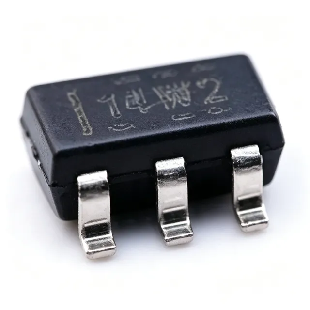
TLV6001IDBVR - 1MHz RRIO Op Amp, 75uA | Texas Instruments
MPN: TLV6001IDBVR ✓ 啟用中TLV6001IDBVR 概覽
An operational amplifier (op amp) is a high-gain differential-input voltage amplifier and one of the most fundamental building blocks of analog signal processing. Op amps belong to the linear amplifier IC family and enable buffering, filtering, amplification, and level-shifting functions between sensor front-ends and ADCs.
Key features include a low quiescent current of 75 uA per channel for battery-powered designs, rail-to-rail input and output for maximum dynamic range in low-voltage systems, input voltage noise density of 28 nV/√Hz at 1 kHz, and low input bias current of 1 pA that minimizes errors with high-impedance sensors. Per TI datasheet, the device is stable with capacitive loads up to 100 pF.
Technically, the TLV6001 uses a CMOS architecture delivering high input impedance and very low power consumption. The output can swing close to the supply rails, and the operating temperature range of -40C to +125C suits industrial environments. The compact SOT-23-5 footprint supports dense PCB layouts.
Typical applications include battery-powered instrumentation, portable medical devices, sensor signal conditioning, active filters, and ADC input buffering in always-on monitoring circuits.
Design tip: decouple with a 0.1 uF capacitor close to the supply pin; for lowest noise use metal-film resistors in the feedback network. As of 2026-08-30, distributor pricing starts near $0.09 (LCSC) to $0.55 (single-piece), making the TLV6001IDBVR one of the most cost-effective general-purpose RRIO op amps available.
直接替換替代品,適用於 TLV6001IDBVR — 相同封裝,腳位對腳位相容。需重新設計 PCB 的不同封裝零件不列入。
此系列的變體
與下列產品可直接替換的同系列型號: TLV6001IDBVR (相同外形與佔位) — 差異在於 Number of Channels, Package, Input Bias Current, Input Voltage Noise Density, MSL Level.
TLV6001IDBVT
✅ 直接替換📋 參考替代品(不在目錄中)
OPA348AIDBVR
✅ 直接替換📋 參考替代品(不在目錄中)
LMV321IDBVR
✅ 直接替換聯絡詢價
查看資料表 →TLV9061IDBVR
✅ 直接替換 ⚠️ 規格未經驗證📋 參考替代品(不在目錄中)
MCP6001T-I/OT
✅ 直接替換📋 參考替代品(不在目錄中)
TLV6001IDBVR 最大額定值與電氣特性
| Number of Channels | 1 |
| Gain-Bandwidth Product | 1 MHz |
| Supply Voltage Range | 1.8 V to 5.5 V |
| Quiescent Current (per channel) | 75 uA |
| Input/Output Type | Rail-to-Rail Input and Output (RRIO) |
| Input Voltage Noise Density | 28 nV/√Hz at 1 kHz |
| Input Bias Current | 1 pA |
| Slew Rate | 0.5 V/us |
| Capacitive Load Stability | Up to 100 pF |
| 工作溫度範圍 | -40C to +125C |
| 封裝 | SOT-23-5 (DBV) |
| 安裝類型 | Surface Mount |
| Architecture | CMOS |
| RoHS 狀態 | Compliant |
| Amplifier Class | General Purpose |
TLV6001IDBVR 腳位配置
| 腳位 1 | OUT — Amplifier output |
| 腳位 2 | V- — Negative supply / ground (single supply) |
| 腳位 3 | IN+ — Non-inverting input |
| 腳位 4 | IN- — Inverting input |
| 腳位 5 | V+ — Positive supply, 1.8 V to 5.5 V |
典型應用
TLV6001IDBVR 適用於 6 應用s: Battery-Powered Sensor Front-End, Portable Medical Devices, ADC Input Buffering, Sensor Signal Conditioning, Active Filter Design, Industrial Analog Interfaces.
Battery-Powered Sensor Front-End
The TLV6001IDBVR's 75 uA quiescent current and 1.8V minimum supply make it ideal for battery-operated sensor nodes where every microamp shortens runtime. The rail-to-rail input accepts signals down to 0V, and the 1 pA bias current avoids loading high-impedance sensors such as piezoelectric or photodiode elements. Placed between the sensor and an ADC, it provides gain and impedance isolation while adding negligible average load; its 1 MHz bandwidth covers signals up to tens of kilohertz with gain, and rail-to-rail output maximizes dynamic range on a 3.3V rail.
推薦
Portable Medical Devices
In portable patient monitors and diagnostic wearables, the TLV6001IDBVR combines low power (75 uA) with rail-to-rail I/O, allowing sensor signals such as bioimpedance or pressure bridge outputs to use nearly the full supply span. The low 1 pA input bias current limits DC errors in high-impedance electrode interfaces, and -40C to +125C operation covers sterilization-adjacent environments. Its compact SOT-23-5 package fits dense wearable PCBs. Unlike lower-cost bipolar op amps, its CMOS input adds no significant bias-induced offset drift, improving measurement repeatability in battery-powered medical signal chains.
推薦
ADC Input Buffering
The TLV6001IDBVR serves as a low-cost buffer between a high-impedance source and a SAR or delta-sigma ADC input. Its 1 MHz gain-bandwidth settles adequately for sampling rates up to roughly 100 ksps at moderate gains, and the rail-to-rail output swings to within millivolts of the rails, preserving codes at full scale. Because it is unity-gain stable with up to 100 pF capacitive load, it tolerates typical ADC input networks with an isolation RC. Pairing it with XAIPART-listed ADCs such as ADS131M08 or ADS1115 yields a complete low-power precision data-acquisition chain.
推薦
Sensor Signal Conditioning
For thermistor, RTD, and resistive-bridge signal conditioning, the TLV6001IDBVR provides inexpensive gain stages and active filtering. The rail-to-rail input handles ground-referenced and mid-rail-biased signals without phase inversion, and 28 nV/√Hz noise is adequate for most industrial sensor resolutions. Its 75 uA draw allows continuous-conditioning designs on 4-20 mA loop budgets and battery transmitters. Configured as a non-inverting amplifier, it supports gains up to about 10 while maintaining useful bandwidth (~100 kHz); as a multiple-feedback low-pass filter, its 1 MHz GBW supports cutoffs to tens of kilohertz with good stopband accuracy.
推薦
Active Filter Design
The TLV6001IDBVR implements Sallen-Key and multiple-feedback active filters in low-cost control and audio-adjacent signal paths. A 1 MHz gain-bandwidth supports a unity-gain second-order filter with cutoffs up to ~100 kHz while keeping Q accuracy within a few percent; below 10 kHz cutoffs, performance is essentially ideal. The rail-to-rail output permits single-supply operation with mid-rail virtual ground, eliminating negative rails. At 75 uA per channel, multi-stage filters remain practical in always-on alarm and monitoring circuits, and the SOT-23-5 footprint allows per-pole placement close to connector inputs for best noise performance.
推薦
Industrial Analog Interfaces
In PLC I/O modules and factory instrumentation, the TLV6001IDBVR scales 0-5V or 0-3.3V sensor signals before digitization. The -40C to +125C industrial temperature range, 5.5V supply tolerance, and robustness to 100 pF capacitive loads suit noisy control-cabinet environments. Its 28 nV/√Hz noise and 1 pA bias support measurement resolutions of millivolts on shunt or bridge signals when paired with instrumentation amplifiers such as the INA237 or AMC1306M25 for isolation. The rail-to-rail output guarantees usable swing into low-voltage ADCs, and its sub-$0.20 volume pricing keeps high-channel-count boards economical.
推薦
推薦產品摘要
工程參考資料,適用於 TLV6001IDBVR — 比較、設計指引及合規資訊。
選型指南
與替代品比較
| 參數 | 本產品 | TLV6001IDBVT | OPA348AIDBVR | LMV321IDBVR | MCP6001T-I/OT |
|---|---|---|---|---|---|
| Package | SOT-23-5 (DBV) | SOT-23-5 - same | SOT-23-5 - same | SOT-23-5 - same | SOT-23-5 - same |
| Brand | Texas Instruments | Texas Instruments | Texas Instruments | Texas Instruments | Microchip Technology |
| Gain-Bandwidth Product | 1 MHz | 1 MHz | 1 MHz | 1 MHz | 1 MHz |
| Quiescent Current | 75 uA | 75 uA | 55 uA | 130 uA | 100 uA |
| Supply Voltage Range | 1.8 V to 5.5 V | 1.8 V to 5.5 V | 2.1 V to 5.5 V | 2.5 V to 5.5 V | 1.8 V to 5.5 V |
| Input Noise Density | 28 nV/√Hz | 28 nV/√Hz | 25 nV/√Hz | 39 nV/√Hz | 28 nV/√Hz |
| Rail-to-Rail I/O | Yes (RRIO) | Yes (RRIO) | Yes (RRIO) | Yes (RRIO) | Yes (RRIO) |
主要差異化特點
- Lowest quiescent current in its 1MHz RRIO class (對比LMV321IDBVR)
- Wider low-end supply range (對比LMV321IDBVR)
- Lower input bias current (對比MCP6001T-I/OT)
設計說明
Place a 0.1 uF ceramic decoupling capacitor within 2-3 mm of pin 5 (V+) with a direct via to the ground plane. Because the SOT-23-5 lead frame inductance is low, high-frequency supply transients couple directly into the output stage; a local capacitor prevents 1 MHz bandwidth from amplifying supply ripple. Avoid routing fast digital traces under the amplifier inputs.
The TLV6001 is unity-gain stable with up to 100 pF capacitive load per the TI datasheet. For larger capacitive loads (cable drives, long traces), add a 10-50 ohm series resistor at pin 1 to isolate the load and preserve phase margin; this costs a few millivolts of output swing at load currents but prevents oscillation.
Do not exceed 5.5V on V+ - there is no internal overvoltage clamp beyond absolute maximum ratings. For AC-coupled single-supply circuits, bias IN+ to mid-rail with a divider and bypass the bias node with at least 0.1 uF; an unbypassed divider injects supply noise directly into the signal path, degrading the 28 nV/√Hz noise floor.
合規資訊
RoHS compliant and lead-free per TI product page and DigiKey/LCSC listings. REACH, halogen-free, and conflict-minerals declarations should be confirmed on the TI quality portal.
