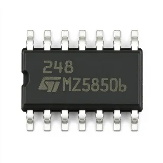
TS339ID - Micropower Quad CMOS Comparator | STMicroelectronics
MPN: TS339ID ✓ 啟用中TS339ID 概覽
A voltage comparator is an analog semiconductor that compares two input voltages and produces a digital logic result indicating which input is higher. The TS339ID belongs to the comparator hierarchy, combining four general-purpose channels in one package. Its CMOS construction reduces current consumption compared with a conventional bipolar LM339, while the open-drain outputs support wired logic, level translation, and systems using external pull-up resistors.
Each channel provides non-inverting and inverting inputs. Key characteristics include extremely low input bias current, a typical input offset current of 1 pA, and typical input impedance of 10^12 ohms. The TS339ID is pin-to-pin and functionally compatible with the bipolar LM339 device. Its typical response time is 1.5 µs for a 5 mV overdrive, making it suitable for threshold detection rather than high-speed signal-chain comparison.
The open-drain output architecture requires an external pull-up resistor when a logic-high level is needed. Because the output stage can pull the node low but cannot actively drive it high, several comparator outputs can be combined in a wired-AND arrangement. This characteristic is useful for supervision, window detection, and fault signaling, although circuit design must account for the pull-up value, output leakage, and bus rise time.
Typical uses include power-supply sequencing, battery monitoring, overvoltage and undervoltage detection, temperature-control thresholds, industrial sensor interfaces, and simple digital control systems. The quad arrangement reduces board area and component count when four independent thresholds are required, particularly in industrial monitoring, instrumentation, and embedded-control equipment.
Designers should verify input common-mode limits, output pull-up requirements, and absolute maximum supply voltage against the manufacturer datasheet before implementation. The open-drain node should include a pull-up to a valid logic rail, and unused inputs must be tied to a defined potential rather than left floating. PCB layout should keep sensitive input traces away from switching nodes and high-current return paths.
This product overview combines the exact TS339ID characteristics with practical guidance for open-drain logic, threshold detection, PCB implementation, and comparison against pin-compatible LM339-family devices. It also organizes the available technical information for engineers evaluating power consumption, response time, input impedance, package compatibility, and lifecycle-sensitive redesigns.
直接替換替代品,適用於 TS339ID — 相同封裝,腳位對腳位相容。需重新設計 PCB 的不同封裝零件不列入。
此系列的變體
與下列產品可直接替換的同系列型號: TS339ID (相同外形與佔位) — 差異在於 Comparator Type, Output Type, Package, Common-Mode Input Range, Input Offset Current.
TS339CD
✅ 直接替換聯絡詢價
查看資料表 →LM339DR
✅ 直接替換聯絡詢價
查看資料表 →LM239DR
✅ 直接替換聯絡詢價
查看資料表 →LM2901DR
✅ 直接替換 ⚠️ 規格未經驗證📋 參考替代品(不在目錄中)
TS339ID 最大額定值與電氣特性
| Comparator Type | Quad general-purpose voltage comparator |
| Technology | CMOS |
| Number of Channels | 4 channels |
| 輸出類型 | Open-drain |
| Supply Voltage Range | ±8 V to ±16 V |
| Typical Supply Current per Comparator | 9 µA |
| Typical Input Offset Current | 1 pA |
| Maximum Input Offset Voltage | 6500 µV |
| Typical Input Bias Current | 0.0006 µA |
| Typical Input Impedance | 10^12 ohms |
| Typical Response Time | 1.5 µs for 5 mV overdrive |
| 工作溫度範圍 | -40 °C to +125 °C |
| 封裝 | 14-pin SOIC |
| 安裝類型 | Surface mount |
| Terminal Count | 14 terminals |
| LM339 Compatibility | Pin-to-pin and functionally compatible with bipolar LM339 |
TS339ID 腳位配置
| 腳位 1 | OUT1 — Comparator 1 open-drain output |
| 腳位 2 | IN1- — Comparator 1 inverting input |
| 腳位 3 | IN1+ — Comparator 1 non-inverting input |
| 腳位 4 | GND — Ground connection |
| 腳位 5 | IN2+ — Comparator 2 non-inverting input |
| 腳位 6 | IN2- — Comparator 2 inverting input |
| 腳位 7 | OUT2 — Comparator 2 open-drain output |
| 腳位 8 | OUT3 — Comparator 3 open-drain output |
| 腳位 9 | IN3- — Comparator 3 inverting input |
| 腳位 10 | IN3+ — Comparator 3 non-inverting input |
| 腳位 11 | IN4+ — Comparator 4 non-inverting input |
| 腳位 12 | IN4- — Comparator 4 inverting input |
| 腳位 13 | OUT4 — Comparator 4 open-drain output |
| 腳位 14 | VCC — Positive supply connection |
典型應用
TS339ID 適用於 6 應用s: Battery Voltage Supervision, Industrial Sensor Threshold Detection, Power Supply Sequencing, Overvoltage and Undervoltage Detection, Temperature Control and Fan Switching, Embedded Control and Logic Interfacing.
Battery Voltage Supervision
The TS339ID fits battery-pack supervision because four comparator channels can monitor multiple pack voltages while each channel typically consumes only 9 µA. Its typical input impedance of 10^12 ohms minimizes loading on high-value resistor dividers, while the 1.5 µs typical response time for a 5 mV overdrive allows quick threshold transitions. A typical implementation compares divided cell or pack voltages against precise references and uses each open-drain output with a pull-up to report an overvoltage, undervoltage, or imbalance condition. The quad package reduces the number of ICs and PCB footprint compared with four single comparators.
推薦
Industrial Sensor Threshold Detection
The TS339ID is suitable for industrial sensor interfaces that convert a slowly changing analog condition into a logic event. Its extremely low typical input bias current of 0.0006 µA and typical input impedance of 10^12 ohms help preserve the accuracy of resistive sensor networks, and its -40 °C to +125 °C operating range supports equipment exposed to varying industrial temperatures. Four channels can monitor discrete sensors without requiring four packages. Open-drain outputs can drive pulled-up status lines, while the 1.5 µs typical response time is adequate for thermal, level, and limit-switch thresholds rather than high-speed waveform detection.
推薦
Power Supply Sequencing
The TS339ID can support power-supply sequencing by comparing feedback voltages from multiple regulated rails and producing discrete enable or fault indications. The 14-pin quad arrangement allows four threshold decisions to be implemented in one IC, with typical comparator consumption of 9 µA helping limit standby overhead. Each open-drain output can act as an active-low status signal when paired with a pull-up, enabling wired fault logic across several rails. Before deployment, verify the input common-mode range, output timing, and logic thresholds because comparator response alone does not guarantee a particular power-up sequence without additional timing and logic circuitry.
推薦
Overvoltage and Undervoltage Detection
Window monitoring benefits from the TS339ID because independent comparator channels can establish upper and lower limits for the same or different voltage rails. Its typical input offset voltage limit of 6500 µV helps define the practical threshold accuracy, while 10^12 ohms typical input impedance reduces divider error. The open-drain outputs can be pulled up to a system logic rail and combined into a fault indication. This makes the device suitable for power modules, embedded systems, and laboratory equipment where an out-of-range input must trigger a digital warning, reset, or shutdown request.
推薦
Temperature Control and Fan Switching
The TS339ID can implement a simple thermal-control decision around a temperature sensor and reference, switching a fan, alarm, or status LED when the monitored level crosses a threshold. The four-channel configuration supports multiple thermal zones or separate over-temperature and under-temperature alarms. Its 1.5 µs typical response time is more than sufficient for ordinary thermal-loop switching, while 9 µA typical consumption per comparator keeps supervisory circuitry lightweight. Because the output is open-drain, it can directly sink the current of a suitably rated indicator or control input when the pull-up and drive limits are respected.
推薦
Embedded Control and Logic Interfacing
The TS339ID is useful in embedded-control boards that need analog thresholds presented to a microcontroller or programmable controller. Four channels provide independent decisions for switches, analog dividers, sensors, or simple oscillators, and the open-drain outputs can be connected to controller interrupt or fault inputs through pull-up resistors. Low input bias current reduces errors in divider networks, and the 9 µA typical consumption per comparator benefits battery-operated equipment. The 1.5 µs typical response time is suitable for control thresholds and event detection, although the design must account for pull-up capacitance and digital-input noise margins.
推薦
推薦產品摘要
工程參考資料,適用於 TS339ID — 比較、設計指引及合規資訊。
選型指南
與替代品比較
| 參數 | 本產品 | TS339CD | LM339DR | LM239DR | LM2901DR |
|---|---|---|---|---|---|
| Package | SOIC-14 | SOIC-14 | SOIC-14 | SOIC-14 | SOIC-14 |
| Brand | STMicroelectronics | STMicroelectronics | Texas Instruments | Texas Instruments | Texas Instruments |
| Comparator Channels | 4 channels | 4 channels | 4 channels | 4 channels | 1 channel |
| Output Architecture | Open-drain | Open-drain | Open-collector | Open-collector | Open-collector |
主要差異化特點
- Lower typical supply consumption than the bipolar LM339 reference (對比LM339DR)
- High input impedance for divider-driven threshold detection (對比LM239DR)
- One package provides four independent comparator channels (對比LM2901DR)
設計說明
The open-drain outputs do not provide a logic-high drive voltage. Add a pull-up resistor to each output that must present a valid high state, and choose its value using the required rise time, bus capacitance, and low-level sink current. Do not connect a pull-up above the output’s absolute maximum voltage or assume that an unused output is self-driving.
Keep the IN+ and IN− traces short and away from switching power nodes, relay contacts, clock edges, and high-current return paths. Comparator inputs are sensitive to nearby switching energy even though the TS339ID has a typical input impedance of 10^12 ohms. Use a continuous ground plane, place the device near its reference network, and avoid routing input traces beneath inductors or boost-converter switch nodes.
Estimate comparator power consumption as P = VS × IS and include the current drawn by pull-up resistors whenever an output is low. For example, a 5 V pull-up that sinks 1 mA adds 5 mW during the asserted state. Verify the power budget and logic levels across the full -40 °C to +125 °C operating range rather than relying only on typical room-temperature characteristics.
Do not leave an unused comparator input floating. Tie both inputs of an unused channel to a defined voltage that remains inside the permitted input common-mode range, while ensuring the output state does not create an unintended system event. This prevents unpredictable switching, excess current, and noise coupling into adjacent channels.
合規資訊
No explicit environmental or automotive qualification statements were identified for TS339ID. The 125 °C maximum operating temperature does not by itself establish AEC-Q100 qualification. Manufacturer documentation should be consulted for final material and process compliance requirements.