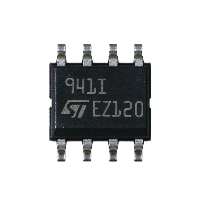
TS941ID - 2.5-10V Rail-to-Rail Op Amp | STMicroelectronics
MPN: TS941ID ✓ 啟用中| 數量 | 單價 | 小計 |
|---|---|---|
| 1 | $1.4063 | $1.41 |
| 10 | $1.0156 | $10.16 |
| 100 | $0.8984 | $89.84 |
| 500 | $0.8594 | $429.70 |
| 1,000 | $0.8203 | $820.30 |
TS941ID 概覽
An operational amplifier, or op amp, is a high-gain differential amplifier used to amplify, buffer, compare, and filter analog signals. The TS941ID sits within the operational-amplifier hierarchy and operates from a 2.5 V to 10 V supply, making it suitable for battery-powered, industrial-control, test-and-measurement, and portable equipment. Its rail-to-rail output stage allows the output voltage to approach the supply limits more closely than a conventional output stage, although the exact output swing and input common-mode behavior must be checked in the manufacturer datasheet for the selected supply voltage.
Key features include a single amplifier configuration, rail-to-rail output, low-noise operation, high input impedance, and very low input-bias current of approximately 1 pA. The 2.5 V minimum supply voltage supports compact, low-energy systems, while the 10 V maximum provides compatibility with common industrial and laboratory supply rails. The manufacturer specifies operation over -40 °C to +85 °C, covering industrial temperature requirements without requiring an automotive-qualified variant.
The TS941ID is intended for general-purpose precision signal conditioning rather than as a high-speed communications amplifier. Its micropower-oriented design is valuable when battery current is important, but the precise quiescent-current value should be taken from the manufacturer datasheet. The approximately 1 pA input-bias current is particularly useful with high-impedance sensors because it limits the DC current drawn through the source resistance and helps reduce input-offset errors.
Typical applications include sensor-signal conditioning, low-current transimpedance buffering, portable instrumentation, industrial measurement, and general analog signal conditioning. In a transimpedance stage, the TS941ID can be paired with a suitable feedback resistor and compensation capacitor while its low input-bias current reduces bias-current-induced error. In instrumentation, it can buffer inputs before a higher-precision converter or provide gain around sensors whose output range does not use the complete supply span.
When designing around the TS941ID, verify input common-mode range, output swing, unity-gain stability, noise, slew rate, and quiescent current against the actual load and supply conditions. Place input, feedback, and decoupling connections for low noise and stable feedback operation, and include adequate output-current margin for capacitive or resistive loads. The 8-pin SOIC footprint is convenient for conventional surface-mount assembly but is not as compact as the smallest QFN packages.
This product page consolidates the verified manufacturer information, distributor availability references, family-level alternatives, parameter comparisons, and practical design guidance. It distinguishes confirmed TS941ID data from specifications that still require confirmation from the manufacturer datasheet, helping engineers identify the part faster without presenting unverified values as established facts.
直接替換替代品,適用於 TS941ID — 相同封裝,腳位對腳位相容。需重新設計 PCB 的不同封裝零件不列入。
快速比較工具 — 選擇替代零件進行並排比較:
TS931ID
聯絡詢價
查看資料表 →TS951ID
聯絡詢價
查看資料表 →TS941LID
📋 參考替代品(不在目錄中)
TS931LID
📋 參考替代品(不在目錄中)
TS951LID
📋 參考替代品(不在目錄中)
TS941ID 最大額定值與電氣特性
| Amplifier Type | Single-circuit general-purpose operational amplifier |
| Number of Circuits | 1 circuit |
| Supply Voltage Range | 2.5 V to 10 V |
| Output Architecture | Rail-to-rail output |
| 工作溫度範圍 | -40 °C to +85 °C |
| 封裝 | 8-pin SOIC |
| 安裝類型 | Surface mount |
| Input Bias Current | Approximately 1 pA |
| Input Impedance | High impedance |
| Noise Characteristics | Low noise |
| Power Classification | Micropower operational amplifier |
| Application Category | General-purpose amplification and signal buffering |
TS941ID 8-pin soic 腳位配置指南
TS941ID(8-pin soic 封裝)的腳位配置。 此類比元件具有輸入、輸出與電源腳位。偏移歸零、補償與致能腳位配置請參閱製造商資料表。適用於訊號調理與放大器電路。

無詳細腳位定義資料: TS941ID.
請參閱 資料表 以查看完整腳位配置。
典型應用
TS941ID 適用於 6 應用s: High-Impedance Sensor Signal Conditioning, Portable Battery-Powered Measurement, Transimpedance Amplifier, Industrial Sensor Interface, Low-Voltage Analog Signal Buffer, Test and Measurement Front End.
High-Impedance Sensor Signal Conditioning
The TS941ID is well suited to conditioning signals from high-impedance sensors because its approximately 1 pA input-bias current limits the error caused by current flowing through a large source resistance. According to the verified distributor information, it combines high input impedance with low-noise operation. Place the amplifier close to the sensor or connector and keep the input trace short to minimize leakage and capacitive pickup. Gain-bandwidth, offset, and common-mode limits are not present in the supplied data, so the sensor resistance, cable length, and operating bandwidth must be checked against the manufacturer datasheet before finalizing the gain and compensation network.
推薦
Portable Battery-Powered Measurement
The TS941ID fits portable measurement systems operating from 2.5 V to 10 V, including handheld analyzers and compact sensor modules. The STMicroelectronics TS94x family is characterized as micropower, while the confirmed 2.5 V minimum supply supports low-voltage battery rails. Rail-to-rail output can provide more useful signal range than a conventional output stage near the supply limits. Because the exact quiescent current was not included in the verified data, battery-life calculations must use the manufacturer’s worst-case value. Designers should also account for the TS941ID’s 8-pin SOIC size and verify stable operation with the intended sensor, filter, and display circuitry.
推薦
Transimpedance Amplifier
The TS941ID can serve as the active element in a transimpedance amplifier for photodiode, electrochemical sensor, or other current-source measurement. Its approximately 1 pA input-bias current is the key benefit because bias current multiplied by feedback resistance creates an offset error that can dominate high-value feedback networks. The 2.5 V to 10 V supply range also supports compact low-voltage sensor systems. Keep the feedback resistor and compensation capacitor close to the amplifier, minimize input-node capacitance, and shield the high-impedance input from moisture and contamination. The exact gain-bandwidth and stability limits are [DATA_NEEDED: TS941ID stability and bandwidth data].
推薦
Industrial Sensor Interface
The TS941ID is appropriate for buffering outputs from industrial sensors that operate from low-voltage rails and have relatively high source impedance. Its high input impedance reduces loading of the sensor, while approximately 1 pA input-bias current limits DC error in high-resistance sensing paths. Rail-to-rail output is useful when the interface must pass signals close to the available 2.5 V to 10 V supply range. The -40 °C to +85 °C operating range supports industrial environments, although it does not by itself establish AEC-Q100 automotive qualification. Confirm electromagnetic-noise margins, isolation requirements, common-mode behavior, and the final calibration path using the official TS941 documentation.
推薦
Low-Voltage Analog Signal Buffer
The TS941ID can buffer a low-voltage analog source before an ADC, display, or control block, preserving signal amplitude through its high input impedance and rail-to-rail output stage. This is particularly useful when a sensor’s output does not cover the complete ADC input range and requires level shifting or gain. The TS941ID’s low-noise characteristic helps avoid degrading weak signals, while the 2.5 V minimum supply supports single-cell and low-voltage systems. Designers should calculate the required gain using verified gain-bandwidth and noise data, which are [DATA_NEEDED: gain-bandwidth and noise parameters]. The source impedance, ADC sampling rate, settling time, and allowable gain error must all be evaluated before selecting the final resistor and capacitor values.
推薦
Test and Measurement Front End
The TS941ID can be used in a general-purpose test-and-measurement front end to buffer probes, scale low-level signals, or drive downstream instrumentation. Its 2.5 V to 10 V supply range accommodates both compact battery-powered testers and conventional laboratory rails, while the approximately 1 pA input-bias current reduces disturbance to high-impedance probes. The rail-to-rail output helps preserve dynamic range, and the 8-pin SOIC package is easy to assemble using standard surface-mount equipment. Verify input capacitance, output drive, slew rate, and stability with the actual cable and load because those values are not included in the supplied search results. A grounded guard or shield may be necessary around high-impedance input nodes.
推薦
推薦產品摘要
工程參考資料,適用於 TS941ID — 比較、設計指引及合規資訊。
選型指南
與替代品比較
| 參數 | 本產品 | TS941LID | TS931ID | TS931LID | TS951ID | TS951LID |
|---|---|---|---|---|---|---|
| Package | 8-pin SOIC | 8-pin SOIC - same | 8-pin SOIC - same | 8-pin SOIC - same | 8-pin SOIC - same | 8-pin SOIC - same |
| Brand | STMicroelectronics | STMicroelectronics | STMicroelectronics | STMicroelectronics | STMicroelectronics | STMicroelectronics |
| Number of Circuits | 1 circuit | 1 circuit | 1 circuit | 1 circuit | 1 circuit | 1 circuit |
| Application Category | General-purpose instrumentation and signal buffering | General-purpose instrumentation and signal buffering | General-purpose instrumentation and signal buffering | General-purpose instrumentation and signal buffering | General-purpose instrumentation and signal buffering | General-purpose instrumentation and signal buffering |
主要差異化特點
- Very low input-bias current supports high-impedance instrumentation (對比LM324D)
- Low 2.5 V minimum supply supports compact low-voltage systems (對比MC1458D)
- Rail-to-rail output increases low-voltage signal utilization (對比TLV1504ID)
- Wide specified industrial temperature range (對比TS941LID)
設計說明
Place the input, feedback, and decoupling components directly adjacent to the TS941ID pins. High-impedance input nodes should be short, clean, and surrounded by grounded copper where practical to reduce leakage and capacitive pickup. The supplied manufacturer information identifies an 8-pin SOIC package but does not include a specific reference layout, so the final arrangement should follow the official TS941 datasheet and account for the package’s exposed supply and ground connections.
Do not assume that rail-to-rail output means the TS941ID accepts every input voltage between the supply rails. The verified data confirms rail-to-rail output and a 2.5 V to 10 V supply range, but the exact input common-mode range and output swing are [DATA_NEEDED]. Check these limits at the actual supply voltage and load. Also verify stable operation with the selected feedback network and output capacitance because gain-bandwidth, slew rate, and unity-gain stability data were not included in the supplied sources.
For battery-powered use, obtain the worst-case quiescent current from the manufacturer datasheet before calculating operating time. The TS94x series is characterized as micropower, but no numeric supply-current value was supplied, so any battery-life estimate would be unsupported. Include sensor current, pull-up or pull-down current, load current, and the efficiency of any upstream regulator in the system budget. Select capacitors and regulator ratings that tolerate the device’s full 2.5 V to 10 V supply range.
The approximately 1 pA input-bias current makes the TS941ID useful with high-source-resistance sensors, but it does not eliminate all error. Bias current multiplied by source resistance creates offset, while input capacitance and leakage can disturb the signal. Use guarding, conformal coating, or a driven guard where necessary, and keep connectors away from moisture and contaminated PCB surfaces. Confirm the noise, offset, and bandwidth specifications in the official datasheet before setting the amplifier gain.
合規資訊
The supplied verified data does not state RoHS, REACH, AEC-Q100, lead-free, halogen-free, or conflict-minerals compliance. These fields remain unknown rather than being inferred from the manufacturer or package.
